首页 > LCA717S > 详情
 Datasheet下载
- 型号: LCA717S
- 制造商: IXYS
- 库位|库存: xxxx|xxxx
- 要求:
| 数量阶梯 | 香港交货 | 国内含税 |
| +xxxx | $xxxx | ¥xxxx |
查看当月历史价格
查看今年历史价格
产品参数
| 参数 | 数值 |
| 产品目录 | 继电器 |
| 描述 | RELAY OPTOMOS 2A SPST-NO 30V |
| 产品分类 | 固态继电器 |
| 品牌 | IXYS Integrated Circuits Division |
| 数据手册 | 点击此处下载产品Datasheet |
| 产品图片 |  |
| 产品型号 | LCA717S |
| rohs | 无铅 / 符合限制有害物质指令(RoHS)规范要求 |
| 产品系列 | LCA, OptoMOS® |
| 产品目录绘图 |  |
| 产品目录页面 | 点击此处下载产品Datasheet |
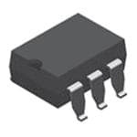
| 供应商器件封装 | 6-SMD |
| 其它名称 | CLA324 |
| 包装 | 管件 |
| 安装类型 | 表面贴装 |
| 导通电阻 | 150 毫欧 |
| 封装/外壳 | 6-SMD(0.300",7.62mm) |
| 标准包装 | 50 |
| 电压-负载 | 0 ~ 30 V |
| 电压-输入 | 1.2VDC |
| 电路 | SPST-NO(1 A 形) |
| 端子类型 | 鸥翼型 |
| 继电器类型 | 继电器 |
| 负载电流 | 2A |
| 输出类型 | AC,DC |
Datasheet
PDF Datasheet 数据手册内容提取
LCA717 Single-Pole, Normally Open OptoMOS® Relay I C D NTEGRATED IRCUITS IVISION Parameter Ratings Units Description Blocking Voltage 30 V The LCA717 is a 30V single-pole, normally open P Load Current 2 A / A (1-Form-A) Solid State Relay. It uses optically rms DC On-Resistance (max) 0.15 coupled MOSFET technology to provide 3750V rms of input to output isolation, and features an ultra-low on-resistance for high-current operation. Features (cid:129) Very Low Maximum On-Resistance: 0.15 Its optically coupled outputs, which use the patented (cid:129) High Load Current: 2A OptoMOS architecture, are controlled by a highly (cid:129) 3750Vrms Input/Output Isolation efficient GaAIAs infrared LED. (cid:129) Low Drive Power Requirements (TTL/CMOS Compatible) Offering the superior reliability associated with (cid:129) No Moving Parts semiconductor devices, the LCA717 can be used to (cid:129) High Reliability replace mechanical relays. Because it has no moving (cid:129) Arc-Free With No Snubbing Circuits parts, it can offer faster, bounce-free switching in a (cid:129) No EMI/RFI Generation more compact surface mount or thru-hole package. (cid:129) Small 6-Pin DIP Package (cid:129) Machine Insertable, Wave Solderable Approvals (cid:129) Surface Mount, Tape & Reel Version Available (cid:129) UL Recognized Component: File E76270 (cid:129) CSA Certified Component: Certificate 1175739 Applications (cid:129) EN/IEC 60950-1 Certified Component: (cid:129) Sensor Circuitry TUV Certificate B 09 07 49410 006 (cid:129) Instrumentation (cid:129) Multiplexers Ordering Information (cid:129) Data Acquisition (cid:129) Electronic Switching Part # Description (cid:129) I/O Subsystems LCA717 6-Pin DIP (50/Tube) (cid:129) Meters (Watt-Hour, Water, Gas) LCA717S 6-Pin Surface Mount (50/Tube) (cid:129) Medical Equipment: Patient/Equipment Isolation LCA717STR 6-Pin Surface Mount (1000/Reel) (cid:129) Aerospace (cid:129) Industrial Controls Pin Configuration AC/DC Configuration Switching Characteristics 1 6 + Control Load of Normally Open Devices 2 5 – Control Do Not Use 3 4 Form-A Do Not Use Load I F DC Only Configuration 90% 1 6 I 10% + Control + Load LOAD t t 2 5 on off – Control – Load 3 4 Do Not Use e Pb 3 DS-LCA717-R04 www.ixysic.com 1
I C D LCA717 NTEGRATED IRCUITS IVISION Absolute Maximum Ratings @ 25ºC Parameter Ratings Units Absolute Maximum Ratings are stress ratings. Stresses in excess of these ratings can cause permanent damage to Blocking Voltage 30 V P the device. Functional operation of the device at conditions Reverse Input Voltage 5 V beyond those indicated in the operational sections of this Input Control Current 50 mA data sheet is not implied. Peak (10ms) 1 A Input Power Dissipation 1 100 mW Total Power Dissipation 2 800 mW Isolation Voltage, Input to Output 3750 V rms Operational Temperature -40 to +85 °C Storage Temperature -40 to +125 °C 1 Derate linearly 1.33 mW / ºC 2 Derate linearly 6.67 mW / ºC Electrical Characteristics @ 25ºC Parameter Conditions Symbol Min Typ Max Units Output Characteristics Load Current, Continuous AC/DC Configuration 2 A / A - I - - rms DC DC Configuration L 4 A DC Peak Load Current t=10ms I - - ±5 A LPK P On-Resistance1 AC/DC Configuration 0.083 0.15 I=1A R - DC Configuration L ON 0.023 0.04 Off-State Leakage Current V=30V I - - 1 µA L P LEAK Switching Speeds Turn-On t 0.92 3 I =5mA, V=10V on - ms Turn-Off F L t 0.44 3 off Output Capacitance V=15V, f=1MHz C - 100 - pF L OUT Input Characteristics Input Control Current to Activate I=1A I - 0.115 2 mA L F Input Control Current to Deactivate - I 0.1 - - mA F Input Voltage Drop I =5mA V 0.9 1.2 1.4 V F F Reverse Input Current V =5V I - - 10 µA R R Common Characteristics Input to Output Capacitance - C - 3 - pF I/O 1 Measurement taken within 1 second of on-time. ESD Rating ESD Rating (Human Body Model) 1000 Volts 2 www.ixysic.com R04
I C D LCA717 NTEGRATED IRCUITS IVISION PERFORMANCE DATA @25ºC (Unless Otherwise Noted)* Typical LED Forward Voltage Drop Typical Turn-On Time Distribution Typical Turn-Off Time Distribution (N=50, I=5mA) (N=50, I=5mA, I=120mA) (N=50, I=5mA, I=120mA) F F L F L 30 25 25 25 20 20 N) N) N) unt ( 20 unt ( 15 unt ( 15 Co 15 Co Co Device 10 Device 10 Device 10 5 5 5 0 0 0 1.215 1.230 1.245 1.260 1.275 1.290 1.305 0.730 0.785 0.840 0.895 0.950 1.005 1.060 0.41 0.42 0.43 0.44 0.45 0.46 LED Forward Voltage (V) Turn-On Time (ms) Turn-Off Time (ms) Typical I for Switch Operation Typical On-Resistance Distribution Blocking Voltage Distribution F (N=50, I=500mA) (N=50, I=2mA, I=1A) (N=50) L F L 25 20 20 20 N) N)15 N)15 Count (15 Count (10 Count (10 Device 10 Device 5 Device 5 5 0 0 0 0.105 0.110 0.115 0.120 0.125 0.130 80.0 81.5 83.0 84.5 86.0 87.5 89.0 36.4 36.7 37.0 37.3 37.6 37.9 38.2 LED Forward Current (mA) On-Resistance (m(cid:58)) Blocking Voltage (V) P Typical LED Forward Voltage Drop Typical Turn-On Time Typical Turn-Off Time vs. Temperature vs. LED Forward Current vs. LED Forward Current 1.6 5000 450 I=50mA ED Forward Voltage (V)11111.....12345 IIF==52mmAA IIFFF==2100mmAA Turn-On Time (s)(cid:80)1234000000000000 Turn-Off Time (s)(cid:80)334479130000 L F I=1mA 1.0 F 0 350 -40 -20 0 20 40 60 80 100 0 10 20 30 40 50 0 10 20 30 40 50 Temperature (ºC) LED Forward Current (mA) LED Forward Current (mA) Typical I for Switch Operation vFs. Temperature Typical Turn-On Time Typical Turn-Off Time (I=1A) vs. Temperature vs. Temperature 0.17 L 4000 700 I=1mA A) 0.16 3500 F 650 m I=1mA urrent ( 00..1145 me (s)(cid:80)23500000 I=2mA me (s)(cid:80) 565000 IFF=2mA ED Forward C 000...111123 Turn-On Ti 112505000000000 IFF=5mA Turn-Off Ti 344550500000 IF=5mA L 0.10 0 300 -40 -20 0 20 40 60 80 100 -40 -20 0 20 40 60 80 100 -40 -20 0 20 40 60 80 100 Temperature (ºC) Temperature (ºC) Temperature (ºC) *The Performance data shown in the graphs above is typical of device performance. For guaranteed parameters not indicated in the written specifications, please contact our application department. R04 www.ixysic.com 3
I C D LCA717 NTEGRATED IRCUITS IVISION PERFORMANCE DATA @25ºC (Unless Otherwise Noted)* Typical On-Resistance Typical Load Current vs. Temperature Maximum Load Current vs. Load Voltage (I=2mA, I=1A) vs. Temperature (I=2mA) F L F 0.12 5 2.0 0.11 DC-Only Configuration (ADC) 1.5 On-Resistance ()(cid:58)0000....00017890 Load Current 1234 AC/DC Configuration (ADC/Arms) Load Current (A)--10001.....05050 0.06 -1.5 0.05 0 -2.0 -40 -20 0 20 40 60 80 100 -40 -20 0 20 40 60 80 100 -0.20-0.15-0.10-0.05 0.00 0.05 0.10 0.15 0.20 Temperature (ºC) Temperature (ºC) Load Voltage (V) Typical Blocking Voltage Typical Leakage vs. Temperature vs. Temperature Measured Across Pins 4&6 (I=1(cid:80)A) (V=30V) Energy Rating Curve L L 39.0 350 8 38.5 300 7 Blocking Voltage (V)P3333366778.....05050 Leakage Current (nA)11220505500000 Load Current (A) 123456 35.5 0 0 -40 -20 0 20 40 60 80 100 -40 -20 0 20 40 60 80 100 10(cid:80)s 100(cid:80)s 1ms 10ms100ms 1s 10s 100s Temperature (ºC) Temperature (ºC) Time *The Performance data shown in the graphs above is typical of device performance. For guaranteed parameters not indicated in the written specifications, please contact our application department. 4 www.ixysic.com R04
I C D LCA717 NTEGRATED IRCUITS IVISION Manufacturing Information Moisture Sensitivity All plastic encapsulated semiconductor packages are susceptible to moisture ingression. IXYS Integrated Circuits Division classified all of its plastic encapsulated devices for moisture sensitivity according to the latest version of the joint industry standard, IPC/JEDEC J-STD-020, in force at the time of product evaluation. We test all of our products to the maximum conditions set forth in the standard, and guarantee proper operation of our devices when handled according to the limitations and information in that standard as well as to any limitations set forth in the information or standards referenced below. Failure to adhere to the warnings or limitations as established by the listed specifications could result in reduced product performance, reduction of operable life, and/or reduction of overall reliability. This product carries a Moisture Sensitivity Level (MSL) rating as shown below, and should be handled according to the requirements of the latest version of the joint industry standard IPC/JEDEC J-STD-033. Device Moisture Sensitivity Level (MSL) Rating LCA717 / LCA717S MSL 1 ESD Sensitivity This product is ESD Sensitive, and should be handled according to the industry standard JESD-625. Reflow Profile This product has a maximum body temperature and time rating as shown below. All other guidelines of J-STD-020 must be observed. Device Maximum Temperature x Time LCA717 / LCA717S 250ºC for 30 seconds Board Wash IXYS Integrated Circuits Division recommends the use of no-clean flux formulations. However, board washing to remove flux residue is acceptable. Since IXYS Integrated Circuits Division employs the use of silicone coating as an optical waveguide in many of its optically isolated products, the use of a short drying bake could be necessary if a wash is used after solder reflow processes. Chlorine- or Fluorine-based solvents or fluxes should not be used. Cleaning methods that employ ultrasonic energy should not be used. e Pb 3 R04 www.ixysic.com 5
I C D LCA717 NTEGRATED IRCUITS IVISION MECHANICAL DIMENSIONS LCA717 8.382 ± 0.381 PCB Hole Pattern 7.239 TYP (0.330 ± 0.015) 2.54 ± 0.127 (0.285 TYP) (0.100 ± 0.005) 6 - 0.800 DIA. 2.540 ± 0.127 (6 - 0.031 DIA.) 9.144 ± 0.508 (0.100 ± 0.005) 6.350 ± 0.127 (0.360 ± 0.020) (0.250 ± 0.005) 7.620 ± 0.127 (0.300 ± 0.005) 7.620 ± 0.254 Pin 1 (0.300 ± 0.010) 1.651 ± 0.254 0.254 ± 0.0127 (0.065 ± 0.010) (0.010 ± 0.0005) 6.350 ± 0.127 5.080 ± 0.127 (0.250 ± 0.005) (0.200 ± 0.005) 3.302 ± 0.051 4.064 TYP (0.130 ± 0.002) (0.160 TYP) Dimensions 0.457 ± 0.076 mm (0.018 ± 0.003) (inches) LCA717S 0.635 ± 0.127 PCB Land Pattern 8.382 ± 0.381 (0.025 ± 0.005) (0.330 ± 0.015) 2.54 ± 0.127 (0.100 ± 0.005) 2.54 (0.10) 9.524 ± 0.508 6.350 ± 0.127 (0.375 ± 0.020) (0.250 ± 0.005) 8.90 1.65 (0.3503) 7.620 ± 0.254 0.254 ± 0.0127 (0.0649) Pin 1 (00..405178 ±± 00..007063) (0.300 ± 0.010) (0.010 ± 0.0005) 1.651 ± 0.254 (0.065 ± 0.010) 0.65 3.302 ± 0.051 (0.130 ± 0.002) (0.0255) 4.445 ± 0.254 (0.175 ± 0.010) Dimensions 1.651 ± 0.254 mm (0.065 ± 0.010) (inches) 6 www.ixysic.com R04
I C D LCA717 NTEGRATED IRCUITS IVISION LCA717STR Tape & Reel 330.2 Dia (13.00 Dia) Top Cover W=16.00 Tape Thickness (0.63) 0.102 Max B = 10.10 (0.004 Max) 0 (0.398) P = 12.00 A = 10.10 K = 4.90 0 0 (0.472) (0.398) (0.19) K = 3.80 Dimensions 1 (0.15) User Direction of Feed mm Embossed (inches) Carrier NOTES: 1. All dimensions carry tolerances of EIA Standard 481-2 Embossment 2. The tape complies with all “Notes” for constant dimensions listed on page 5 of EIA-481-2 For additional information please visit our website at: www.ixysic.com IXYS Integrated Circuits Division makes no representations or warranties with respect to the accuracy or completeness of the contents of this publication and reserves the right to make changes to specifications and product descriptions at any time without notice. Neither circuit patent licenses nor indemnity are expressed or implied. Except as set forth in IXYS Integrated Circuits Division’s Standard Terms and Conditions of Sale, IXYS Integrated Circuits Division assumes no liability whatsoever, and disclaims any express or implied warranty, relating to its products including, but not limited to, the implied warranty of merchantability, fitness for a particular purpose, or infringement of any intellectual property right. The products described in this document are not designed, intended, authorized or warranted for use as components in systems intended for surgical implant into the body, or in other applications intended to support or sustain life, or where malfunction of IXYS Integrated Circuits Division’s product may result in direct physical harm, injury, or death to a person or severe property or environmental damage. IXYS Integrated Circuits Division reserves the right to discontinue or make changes to its products at any time without notice. Specification: DS-LCA717-R04 ©Copyright 2012, IXYS Integrated Circuits Division OptoMOS® is a registered trademark of IXYS Integrated Circuits Division All rights reserved. Printed in USA. 7 12/22/2012
Mouser Electronics Authorized Distributor Click to View Pricing, Inventory, Delivery & Lifecycle Information: I XYS: LCA717S LCA717 LCA717STR