ICGOO在线商城 > 集成电路(IC) > PMIC - 电机驱动器,控制器 > LB1973JA-ZH

 Datasheet下载
- 型号: LB1973JA-ZH
- 制造商: ON Semiconductor
- 库位|库存: xxxx|xxxx
- 要求:
| 数量阶梯 | 香港交货 | 国内含税 |
| +xxxx | $xxxx | ¥xxxx |
查看当月历史价格
查看今年历史价格
LB1973JA-ZH产品简介:
ICGOO电子元器件商城为您提供LB1973JA-ZH由ON Semiconductor设计生产,在icgoo商城现货销售,并且可以通过原厂、代理商等渠道进行代购。 LB1973JA-ZH价格参考¥8.15-¥8.15。ON SemiconductorLB1973JA-ZH封装/规格:PMIC - 电机驱动器,控制器, Bipolar Motor Driver Bipolar Parallel 16-SSOP。您可以下载LB1973JA-ZH参考资料、Datasheet数据手册功能说明书,资料中有LB1973JA-ZH 详细功能的应用电路图电压和使用方法及教程。
ON Semiconductor(安森美)的LB1973JA-ZH是一款直流电机驱动器,属于PMIC中的电机驱动控制器类别。该芯片主要用于小型直流电机的控制,具有H桥驱动结构,可实现电机正反转及制动功能,适用于低电压、小电流的应用场景。

典型应用场景包括:便携式电子产品中的微型电机驱动,如数码相机的镜头对焦/变焦机构、自动光圈控制、小型打印机的进纸电机控制、玩具机器人关节驱动、家用电器中的小型风扇或阀门控制等。此外,也常用于办公设备如扫描仪、小型投影仪中的机械运动部件控制。

LB1973JA-ZH采用小型化封装,功耗低,集成度高,具备过热保护和防止电源反接等功能,提升了系统可靠性。其工作电压范围较宽(通常为2.7V至16V),适合电池供电设备,广泛应用于消费电子、工业控制及智能家居等领域中需要精密控制小型直流电机的场合。
| 参数 | 数值 |
| 产品目录 | 集成电路 (IC)半导体 |
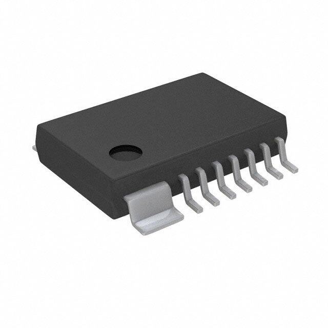
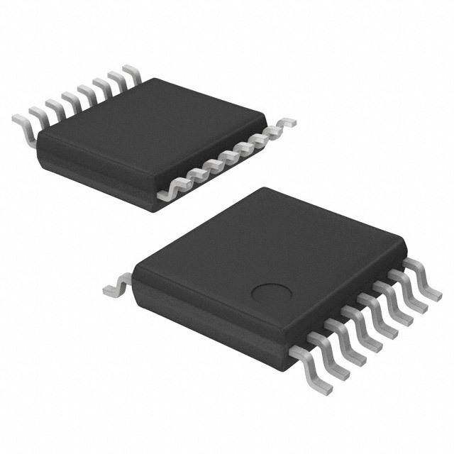
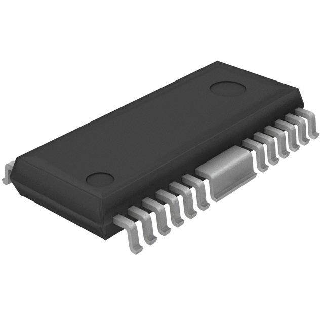
| 描述 | IC MOTOR DRIVER PAR 16SSOP马达/运动/点火控制器和驱动器 GP DC MOTOR DRIVER |
| 产品分类 | PMIC - 电机, 电桥式驱动器集成电路 - IC |
| 品牌 | ON Semiconductor |
| 产品手册 | |
| 产品图片 |
|
| rohs | 符合RoHS无铅 / 符合限制有害物质指令(RoHS)规范要求 |
| 产品系列 | 电源管理 IC,马达/运动/点火控制器和驱动器,ON Semiconductor LB1973JA-ZH- |
| 数据手册 | |
| 产品型号 | LB1973JA-ZH |
| 产品 | Fan / Motor Controllers / Drivers |
| 产品培训模块 | http://www.digikey.cn/PTM/IndividualPTM.page?site=cn&lang=zhs&ptm=26174 |
| 产品种类 | 马达/运动/点火控制器和驱动器 |
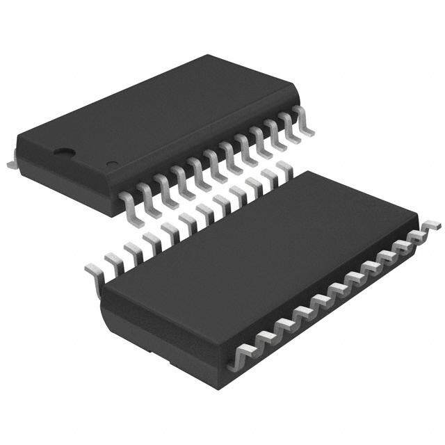
| 供应商器件封装 | 16-SSOP |
| 其它名称 | LB1973JA-ZH-ND |
| 功率耗散 | 800 mW |
| 功能 | 驱动器 - 全集成,控制和功率级 |
| 包装 | 带盒(TB) |
| 商标 | ON Semiconductor |
| 安装类型 | 表面贴装 |
| 安装风格 | SMD/SMT |
| 封装 | Bulk |
| 封装/外壳 | 16-LSSOP (0.173", 4.40mm 宽) |
| 封装/箱体 | SSOP-16 |
| 工作温度 | -20°C ~ 85°C |
| 工作电源电压 | 1.8 V to 7.5 V |
| 工厂包装数量 | 90 |
| 应用 | 照相机 |
| 接口 | 并联 |
| 标准包装 | 90 |
| 电压-电源 | 1.8 V ~ 7.5 V |
| 电压-负载 | 1.8 V ~ 7.5 V |
| 电机类型-AC,DC | - |
| 电机类型-步进 | 双极性 |
| 电流-输出 | 1A |
| 电源电流 | 1 uA |
| 类型 | 2 Channel H-Bridge Motor Driver |
| 系列 | LB1973JA |
| 输出配置 | 全 H 桥,(2) 双 |


- 商务部:美国ITC正式对集成电路等产品启动337调查
- 曝三星4nm工艺存在良率问题 高通将骁龙8 Gen1或转产台积电
- 太阳诱电将投资9.5亿元在常州建新厂生产MLCC 预计2023年完工
- 英特尔发布欧洲新工厂建设计划 深化IDM 2.0 战略
- 台积电先进制程称霸业界 有大客户加持明年业绩稳了
- 达到5530亿美元!SIA预计今年全球半导体销售额将创下新高
- 英特尔拟将自动驾驶子公司Mobileye上市 估值或超500亿美元
- 三星加码芯片和SET,合并消费电子和移动部门,撤换高东真等 CEO
- 三星电子宣布重大人事变动 还合并消费电子和移动部门
- 海关总署:前11个月进口集成电路产品价值2.52万亿元 增长14.8%

PDF Datasheet 数据手册内容提取
Ordering number : ENA2014 LB1973JA M onolithic Digital IC T wo-channel H-Bridge Driver http://onsemi.com Overview The LB1973JA is a two-channel H-bridge driver that supports for low saturation draive operation. It is optimal for H-bridge drive of stepping motors (AF and zoom) in portable equipment such as camera cell phones. Features • Two-channel H-bridge driver • 2 phase excitation, 1-2 phase excitation drive are possible • 2ch simultaneous connection is possible • The range of the operation voltage is wide.(1.8V to 7.5V) • Parallel input interface • Built-in thermal protection Specifications Absolute Maximum Ratings at Ta = 25°C Parameter Symbol Conditions Ratings Unit Maximum supply voltage VCC max -0.3 to +8.0 V Output voltage VOUT max - VSF to VCC+VSF V Input voltage VIN max -0.3 to +8.0 V Spark killer Di order direction electric ISF max 1000 mA Ground pin source current IGND Per channel 1000 mA Allowable power dissipation Pd max *Mounted on a bord 800 mW Operating temperature Topr -20 to +85 °C Storage temperature Tstg -40 to +150 °C * Mounted on a Specified board : 114.3mm×76.1mm×1.6mm, glass epoxy Caution 1) Absolute maximum ratings represent the value which cannot be exceeded for any length of time. Caution 2) Even when the device is used within the range of absolute maximum ratings, as a result of continuous usage under high temperature, high current, high voltage, or drastic temperature change, the reliability of the IC may be degraded. Please contact us for the further details. StressesexceedingMaximumRatingsmaydamagethedevice.MaximumRatingsarestressratingsonly.FunctionaloperationabovetheRecommendedOperating Conditions is not implied. Extended exposure to stresses above the Recommended Operating Conditions may affect device reliability. Allowable Operating Ratings at Ta = 25°C Parameter Symbol Conditions Ratings Unit Supply voltage VCC 1.8 to 7.5 V High-level input voltage VIH RIN = 1kΩ 1.3 to 7.5 V Low-level input voltage VIL RIN = 1kΩ -0.3 to +0.5 V Semiconductor Components Industries, LLC, 2013 June, 2013 30712 SY 20120117-S00010 No.A2014-1/5
LB1973JA Electrical Characteristics at Ta = 25°C, VCC = 1.9V Ratings Parameter Symbol Conditions Unit min typ max Source current ICCO1 VCC = 1.9V,IN1 to IN4 = Low level 0.01 1 μA ICCO2 VCC = 3V,IN1 to IN4 = Low level 0.01 1 μA ICC1 IN1 = High level,IN2 to IN4 = Low level 18 25 mA ICC2 IN1 = High level,IN2 to IN4 = Low level, 19 27.5 mA VCC = 3V Output saturation voltage1 VOUT11 IOUT = 270mA,VCC = 1.9V to 3.6V, 0.2 0.3 V (single connection) Ta = -20 to 85°C VOUT = Upper Tr and Under Tr IN1 = High level, IN2 to IN4 = Low level Supplementation: Standard similar as for IN2 to IN4 = High level VOUT12 IOUT = 350mA,VCC = 1.9V to 3.6V, 0.25 0.4 V Ta = -20 to 85°C VOUT = Upper Tr and Under Tr IN1 = High level, IN2 to IN4 = Low level Supplementation: Standard similar as for IN2 to IN4 = High level Output saturation voltage2 VOUT21 IOUT = 270mA,VCC = 1.9V to 3.6V, 0.12 0.2 V (parallel connection) Ta = -20 to 85°C VOUT = Upper Tr and Under Tr OUT1-3,OUT2-4 short. IN1 and IN3 = High level, IN2 and IN4 = Low level Supplementation: Standard similar as for IN2 and IN4 = High level VOUT22 IOUT = 500mA,VCC = 1.9V to 3.6V, 0.2 0.35 V Ta = -20 to 85°C VOUT = Upper Tr and Under Tr OUT1-3,OUT2-4 short. IN1 and IN3 = High level,IN2 and IN4 = Low level Supplementation: Standard similar as for IN2 and IN4 = High level Output electric current with the IPA VIN = 1.9 to 3.6V, Ta = -20 to 85°C *1 9 mA parasitic element Input current IIN VIN = 1.9V 32 70 μA Themal shutdown operation Ttsd *2: Design guarantee 140 °C temperature Temperature hysteresis width ∆T *2: Design guarantee 20 °C Spark killer Diode Reverse current IS(leak) VCC-OUT = 8V, VIN = Low level 10 μA Forword voltage VSF ISF = 400mA, VIN = Low level 1.7 V *1: Output electric current with the parasitic element_IPA: The current value that the off ch(-free) output is pulled at the time of one side ch drive by a parasitic element *2: Design guarantee value and does not measure * VSF: The current order direction voltage true in a time No.A2014-2/5
LB1973JA Package Dimensions unit : mm (typ) 3178B Pd max -- Ta 1.0 5.2 Mounted on a specified board : W 114.3mm x 76.1mm x 1.6mm 16 9 ax - 0.8 glass epoxy m d P 4.4 6.4 pation, 0.6 si 0.5 wer dis 0.4 1 8 o p (0.33) 0.65 0.22 0.15 wable 0.2 o max All 1.5 0-20 0 20 40 60 8085 100 1.3) Ambient temperature, Ta -- C ( 1 0. SANYO :SSOP16(225mil) Pin Assignment T4 T3 T1 T2 D C U U C U U C N N O O N O O N G 16 15 14 13 12 11 10 9 1 2 3 4 5 6 7 8 C C 4 3 C 1 2 C VC N IN IN N IN IN N (Top View) Truth Table Input Output Mode IN1 IN2 IN3 IN4 OUT1 OUT2 OUT3 OUT4 Low Low Low Low Off Off Off Off Standby mode High Low High Low Channel 1, forward - - - - Low High Low High Channel 1, reverse High Low High Low Channel 2, forward - - - - Low High Low High Channel 2, reverse High High - - The logic output for the first high-level input is produced. - - High High No.A2014-3/5
LB1973JA Stepping motor control example (1) Timing chart for 2-phase drive IN1 IIN2 IN3 IN4 Channel 1 Standby Forward Reverse Forward Reverse Forward Standby output mode Channel 2 Standby Forward Reverse Forward Reverse Forward Standby output mode (2) Timing chart for 1-2 phase drive IN1 IIN2 IN3 IN4 Channel 1 Standby Forward OFF Reverse OFF Forward Standby output mode Channel 2 Standby Forward OFF Reverse OFF Forward Standby output mode No.A2014-4/5
LB1973JA Block Diagram VCC 30K OUT2 IN2 100K T h C e on rm OUT1 IN1 13000KK trol Blo al shutd ck C own IN3 30K ircu cir OUT3 it cu 100K it OUT4 30K IN4 100K GND ONSemiconductorandtheONlogoareregisteredtrademarksofSemiconductorComponentsIndustries,LLC(SCILLC).SCILLCownstherightstoanumber of patents, trademarks, copyrights, trade secrets, and other intellectual property. A listing of SCILLC’s product/patent coverage may be accessed at www.onsemi.com/site/pdf/Patent-Marking.pdf.SCILLCreservestherighttomakechangeswithoutfurthernoticetoanyproductsherein.SCILLCmakesno warranty,representationorguaranteeregardingthesuitabilityofitsproductsforanyparticularpurpose,nordoesSCILLCassumeanyliabilityarisingoutofthe applicationoruseofanyproductorcircuit,andspecificallydisclaimsanyandallliability,includingwithoutlimitationspecial,consequentialorincidental damages.“Typical”parameterswhichmaybeprovidedinSCILLCdatasheetsand/orspecificationscananddovaryindifferentapplicationsandactual performancemayvaryovertime.Alloperatingparameters,including“Typicals” mustbevalidatedforeachcustomerapplicationbycustomer’stechnical experts.SCILLCdoesnotconveyanylicenseunderitspatentrightsnortherightsofothers.SCILLCproductsarenotdesigned,intended,orauthorizedforuse ascomponentsinsystemsintendedforsurgicalimplantintothebody,orotherapplicationsintendedtosupportorsustainlife,orforanyotherapplicationin whichthefailureoftheSCILLCproductcouldcreateasituationwherepersonalinjuryordeathmayoccur.ShouldBuyerpurchaseoruseSCILLCproductsfor anysuchunintendedorunauthorizedapplication,BuyershallindemnifyandholdSCILLCanditsofficers,employees,subsidiaries,affiliates,anddistributors harmlessagainstallclaims,costs,damages,andexpenses,andreasonableattorneyfeesarisingoutof,directlyorindirectly,anyclaimofpersonalinjuryor deathassociatedwithsuchunintendedorunauthorizeduse,evenifsuchclaimallegesthatSCILLCwasnegligentregardingthedesignormanufactureofthe part. SCILLC is an Equal Opportunity/Affirmative Action Employer. This literature is subject to all applicable copyright laws and is not for resale in any manner. PS No.A2014-5/5