ICGOO在线商城 > 集成电路(IC) > PMIC - 稳压器 - 线性 > L79L05ACUTR
 Datasheet下载
- 型号: L79L05ACUTR
- 制造商: STMicroelectronics
- 库位|库存: xxxx|xxxx
- 要求:
| 数量阶梯 | 香港交货 | 国内含税 |
| +xxxx | $xxxx | ¥xxxx |
查看当月历史价格
查看今年历史价格
L79L05ACUTR产品简介:
ICGOO电子元器件商城为您提供L79L05ACUTR由STMicroelectronics设计生产,在icgoo商城现货销售,并且可以通过原厂、代理商等渠道进行代购。 L79L05ACUTR价格参考¥0.72-¥0.95。STMicroelectronicsL79L05ACUTR封装/规格:PMIC - 稳压器 - 线性, Linear Voltage Regulator IC 1 Output 100mA SOT-89-3。您可以下载L79L05ACUTR参考资料、Datasheet数据手册功能说明书,资料中有L79L05ACUTR 详细功能的应用电路图电压和使用方法及教程。
| 参数 | 数值 |
| 产品目录 | 集成电路 (IC)半导体 |
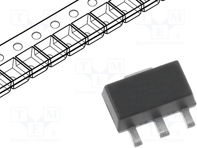
| 描述 | IC REG LDO -5V 0.1A SOT89-3线性稳压器 5.0V 0.1A Negative |
| 产品分类 | |
| 品牌 | STMicroelectronics |
| 产品手册 | |
| 产品图片 |
|
| rohs | 符合RoHS无铅 / 符合限制有害物质指令(RoHS)规范要求 |
| 产品系列 | 电源管理 IC,线性稳压器,STMicroelectronics L79L05ACUTR- |
| 数据手册 | |
| 产品型号 | L79L05ACUTR |
| PSRR/纹波抑制—典型值 | 49 dB |
| 产品目录页面 | |
| 产品种类 | |
| 供应商器件封装 | SOT-89-3 |
| 其它名称 | 497-1219-1 |
| 其它有关文件 | http://www.st.com/web/catalog/sense_power/FM142/CL1015/SC316/PF68123?referrer=70071840 |
| 包装 | 剪切带 (CT) |
| 商标 | STMicroelectronics |
| 安装类型 | 表面贴装 |
| 安装风格 | SMD/SMT |
| 封装 | Reel |
| 封装/外壳 | TO-243AA |
| 封装/箱体 | SOT-89 |
| 工作温度 | 0°C ~ 125°C |
| 工厂包装数量 | 2500 |
| 最大工作温度 | + 125 C |
| 最大输入电压 | - 30 V |
| 最小工作温度 | 0 C |
| 最小输入电压 | - 7 V |
| 极性 | Negative |
| 标准包装 | 1 |
| 电压-跌落(典型值) | 1.7V @ 40mA |
| 电压-输入 | 可下调至 -30V |
| 电压-输出 | -5V |
| 电流-输出 | 100mA |
| 电流-限制(最小值) | - |
| 稳压器拓扑 | 负,固定式 |
| 稳压器数 | 1 |
| 系列 | L79L05AC |
| 线路调整率 | 150 mV |
| 负载调节 | 60 mV |
| 输出电压 | - 5 V |
| 输出电流 | 0.1 A |
| 输出端数量 | 1 |
| 输出类型 | Fixed |


- 商务部:美国ITC正式对集成电路等产品启动337调查
- 曝三星4nm工艺存在良率问题 高通将骁龙8 Gen1或转产台积电
- 太阳诱电将投资9.5亿元在常州建新厂生产MLCC 预计2023年完工
- 英特尔发布欧洲新工厂建设计划 深化IDM 2.0 战略
- 台积电先进制程称霸业界 有大客户加持明年业绩稳了
- 达到5530亿美元!SIA预计今年全球半导体销售额将创下新高
- 英特尔拟将自动驾驶子公司Mobileye上市 估值或超500亿美元
- 三星加码芯片和SET,合并消费电子和移动部门,撤换高东真等 CEO
- 三星电子宣布重大人事变动 还合并消费电子和移动部门
- 海关总署:前11个月进口集成电路产品价值2.52万亿元 增长14.8%


PDF Datasheet 数据手册内容提取
L79L Negative voltage regulators Datasheet - production data Description The L79L series of three-terminal negative regulators employ internal current limiting and thermal shutdown, making them essentially indestructible. If adequate heat-sink is provided, they can deliver up to 100 mA output current. They are intended as fixed voltage regulators in a wide range of applications including local or on- card regulation for elimination of noise and distribution problems associated with single-point regulation. In addition, they can be used with power pass elements to make high-current voltage regulators. The L79L series used as Features Zener diode/resistor combination replacement, Output current up to 100 mA offers an effective output impedance Output voltages of -5; -8;-12; -15 V improvement of typically two orders of magnitude, along with lower quiescent current and lower Thermal overload protection noise. Short-circuit protection No external components are required Output tolerance + 4% December 2017 DocID2511 Rev 19 1/23 This is information on a product in full production. www.st.com
Contents L79L Contents 1 Diagram ............................................................................................ 3 2 Pin configuration ............................................................................. 4 3 Maximum ratings ............................................................................. 5 4 Electrical characteristics ................................................................ 6 5 Package information ....................................................................... 9 5.1 TO-92 package information ............................................................... 9 5.2 TO-92 packing information .............................................................. 10 5.3 TO-92 Ammopak packing information ............................................. 12 5.4 SO-8 package information .............................................................. 14 5.5 SO-8 packing information ................................................................ 16 5.6 SOT-89 package information .......................................................... 17 5.7 SOT-89 packing information............................................................ 20 6 Ordering information ..................................................................... 21 7 Revision history ............................................................................ 22 2/23 DocID2511 Rev 19
L79L Diagram 1 Diagram Figure 1: Schematic diagram DocID2511 Rev 19 3/23
Pin configuration L79L 2 Pin configuration Figure 2: Pin connection (top view, bottom view for TO-92) Figure 3: Test circuit 4/23 DocID2511 Rev 19
L79L Maximum ratings 3 Maximum ratings Table 1: Absolute maximum ratings Symbol Parameter Value Unit VO = -5 to -9 V -30 VI DC input voltage V VO = -12 to -15 V -35 IO Output current 100 mA PD Power dissipation Internally limited (1) mW TSTG Storage temperature range -40 to 150 °C For L79LXXAC 0 to 125 TOP Operating junction temperature range °C For L79LXXAB -40 to 125 Notes: (1) Our SO-8 package used for Voltage Regulators is modified internally to have pins 2, 3, 6 and 7 electrically communed to the die attach flag. This particular frame decreases the total thermal resistance of the package and increases its ability to dissipate power when an appropriate area of copper on the printed circuit board is available for heat-sinking. The external dimensions are the same as for the standard SO-8. Table 2: Thermal data Symbol Parameter SO-8 TO-92 SOT-89 Unit RthJC Thermal resistance junction-case (max.) 20 15 °C/W RthJA Thermal resistance junction-ambient (max.) 55 (1) 200 115 °C/W Notes: (1) Considering 6 cm2 of copper Board heat-sink. DocID2511 Rev 19 5/23
Electrical characteristics L79L 4 Electrical characteristics Refer to the test circuits, V = - 10 V, I = 40 mA, C = 0.33 μF, C = 0.1 μF, T = 0 I O I O J to 125 °C for L79L05AC, T = -40 to 125 °C for L79L05AB, unless otherwise specified. J Table 3: Electrical characteristics of L79L05AC and L79L05AB Symbol Parameter Test conditions Min. Typ. Max. Unit VO Output voltage TJ = 25 °C -4.8 -5 -5.2 V - - IO = 1 to 40 mA, VI = -7 to -20 V 4.75 5.25 VO Output voltage V - - IO = 1 to 70 mA, VI = -10 V 4.75 5.25 VI = -7 to -20 V, TJ = 25 °C 150 ΔVO Line regulation mV VI = -8 to -20 V, TJ = 25 °C 100 IO = 1 to 100 mA, TJ = 25 °C 60 ΔVO Load regulation mV IO = 1 to 40 mA, TJ = 25 °C 30 TJ = 25 °C 6 mA Id Quiescent current TJ = 125 °C 5.5 mA Quiescent current IO = 1 to 40 mA 0.1 ΔId change VI = -8 to -20 V 1.5 mA eN Output noise voltage B = 10 Hz to 100 kHz, TJ = 25 °C 40 µV SVR Supply voltage VI = -8 to -18 V, f = 120 Hz IO = 40 41 49 dB rejection mA, TJ = 25 °C Vd Dropout voltage 1.7 V Refer to the test circuits, V = - 14 V, I = 40 mA, C = 0.33 μF, C = 0.1 μF, T = 0 I O I O J to 125 °C for L79L08AC T = -40 to 125 °C for L79L08AB, unless otherwise specified. J Table 4: Electrical characteristics of L79L08AC and L79L08AB Symbol Parameter Test conditions Min. Typ. Max. Unit - - VO Output voltage TJ = 25 °C 7.68 -8 8.32 V IO = 1 to 40 mA, VI = -10.5 to -23 V -7.6 -8.4 VO Output voltage V IO = 1 to 70 mA, VI = -14 V -7.6 -8.4 VI = -10.5 to -23 V, TJ = 25 °C 175 ΔVO Line regulation mV VI = -11 to -23 V, TJ = 25 °C 125 IO = 1 to 100 mA, TJ = 25 °C 80 ΔVO Load regulation mV IO = 1 to 40 mA, TJ = 25 °C 40 TJ = 25 °C 6 mA Id Quiescent current TJ = 125 °C 5.5 mA Quiescent current IO = 1 to 40 mA 0.1 ΔId change VI = -11 to -23 V 1.5 mA Output noise eN voltage B = 10 Hz to 100 kHz, TJ = 25 °C 60 µV 6/23 DocID2511 Rev 19
L79L Electrical characteristics Symbol Parameter Test conditions Min. Typ. Max. Unit SVR Supply voltage VI = -12 to -23 V, f = 120 Hz, IO = 40 37 45 dB rejection mA, TJ = 25 °C Vd Dropout voltage 1.7 V Refer to the test circuits, V = - 19 V, I = 40 mA, C = 0.33 μF, C = 0.1 μF, T = 0 to 125 I O I O J °C for L79L12AC, T = -40 to 125 °C for L79L12AB, unless otherwise specified. J Table 5: Electrical characteristics of L79L12AC and L79L12AB Symbol Parameter Test conditions Min. Typ. Max. Unit VO Output voltage TJ = 25°C -11.5 -12 -12.5 V IO = 1 to 40 mA, VI = -14.5 -11.4 -12.6 VO Output voltage to -27 V V IO = 1 to 70 mA, VI = -19 V -11.4 -12.6 VI = -14.5 to -27 V, TJ = 25 °C 250 ΔVO Line regulation mV VI = -16 to -27 V, TJ = 25 °C 200 IO = 1 to 100 mA, TJ = 25 °C 100 ΔVO Load regulation mV IO = 1 to 40 mA, TJ = 25 °C 50 TJ = 25 °C 6.5 mA Id Quiescent current TJ = 125 °C 6 mA Quiescent current IO = 1 to 40 mA 0.1 ΔId change VI = -16 to -27 V 1.5 mA Output noise B = 10 Hz to 100 kHz, eN 80 µV voltage TJ = 25 °C SVR Supply voltage VI = -15 to -25 V, f = 120 Hz 37 42 dB rejection IO = 40 mA, TJ = 25 °C Vd Dropout voltage 1.7 V Refer to the test circuits, V = - 23 V, I = 40 mA, C = 0.33 μF, C = 0.1 μF, T = 0 I O I O J to 125 °C for L79L15AC, T = -40 to 125 °C for L79L15AB, unless otherwise specified. J Table 6: Electrical characteristics of L79L15AC and L79L15AB Symbol Parameter Test conditions Min. Typ. Max. Unit VO Output voltage TJ = 25°C -14.4 -15 -15.6 V IO = 1 to 40 mA, VI = -17.5 -14.25 -15.75 VO Output voltage to -30 V V IO = 1 to 70 mA, VI = -23 V -14.25 -15.75 VI = -17.5 to -30 V, TJ = 25 °C 300 ΔVO Line regulation mV VI = -20 to -30 V, TJ = 25 °C 250 IO = 1 to 100 mA, TJ = 25 °C 150 ΔVO Load regulation mV IO = 1 to 40 mA, TJ = 25 °C 75 TJ = 25 °C 6.5 mA Id Quiescent current TJ = 125 °C 6 mA Quiescent current IO = 1 to 40 mA 0.1 ΔId change VI = -20 to -30 V 1.5 mA DocID2511 Rev 19 7/23
Electrical characteristics L79L Symbol Parameter Test conditions Min. Typ. Max. Unit Output noise B = 10 Hz to 100 kHz, eN 90 µV voltage TJ = 25 °C Supply voltage VI = -18.5 to -28.5.V, SVR rejection f = 120 Hz IO = 40 mA, 34 39 dB TJ = 25 °C Vd Dropout voltage 1.7 V 8/23 DocID2511 Rev 19
L79L Package information 5 Package information In order to meet environmental requirements, ST offers these devices in different grades of ECOPACK® packages, depending on their level of environmental compliance. ECOPACK® specifications, grade definitions and product status are available at: www.st.com. ECOPACK® is an ST trademark. 5.1 TO-92 package information Figure 4: TO-92 package outline Table 7: TO-92 mechanical data mm Dim. Min. Typ. Max. A 4.32 4.95 b 0.36 0.51 D 4.45 4.95 E 3.30 3.94 e 2.41 2.67 e1 1.14 1.40 L 12.70 15.49 R 2.16 2.41 S1 0.92 1.52 W 0.41 0.56 V 5° DocID2511 Rev 19 9/23
Package information L79L 5.2 TO-92 packing information Figure 5: TO-92 tape and reel outline 10/23 DocID2511 Rev 19
L79L Package information Table 8: TO-92 tape and reel mechanical data mm Dim. Min. Typ. Max. A1 4.80 T 3.80 T1 1.60 T2 2.30 d 0.45 0.47 0.48 P0 12.50 12.70 12.90 P2 5.65 6.35 7.05 F1, F2 2.40 2.50 2.94 F3 4.98 5.08 5.48 delta H -2.00 2.00 W 17.50 18.00 19.00 W0 5.5 6.00 6.5 W1 8.50 9.00 9.25 W2 0.50 H 18.50 21 H3 0.5 1 2 H0 15.50 16.00 18.8 H1 25.0 27.0 D0 3.80 4.00 4.20 t 0.90 L 11.00 I1 3.00 delta P -1.00 1.00 Ø1 352 355 358 Ø2 28 30 32 u 44 47 50 DocID2511 Rev 19 11/23
Package information L79L 5.3 TO-92 Ammopak packing information Figure 6: TO-92 Ammopak tape and reel outline 12/23 DocID2511 Rev 19
L79L Package information Table 9: TO-92 Ammopak tape and reel mechanical data mm Dim. Min. Typ. Max. A1 4.80 T 3.80 T1 1.60 T2 2.30 d 0.45 0.47 0.48 P0 12.50 12.70 12.90 P2 5.65 6.35 7.05 F1, F2 2.40 2.50 2.94 F3 4.98 5.08 5.48 delta H -2.00 2.00 W 17.50 18.00 19.00 W0 5.5 6.00 6.5 W1 8.50 9.00 9.25 W2 0.50 H 18.50 21 H3 0.5 1 2 H0 15.50 16.00 18.8 H1 25.0 27.0 D0 3.80 4.00 4.20 t 0.90 L 11.00 I1 3.00 delta P -1.00 1.00 DocID2511 Rev 19 13/23
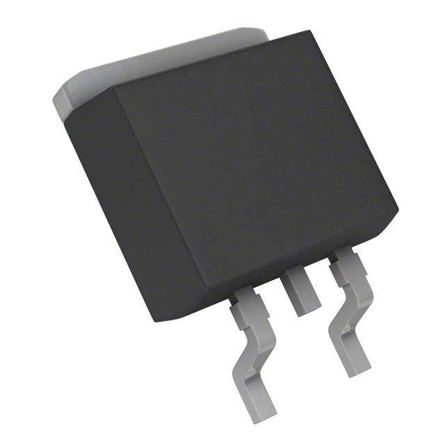
Package information L79L 5.4 SO-8 package information Figure 7: SO-8 package outline 14/23 DocID2511 Rev 19
L79L Package information Table 10: SO-8 mechanical data mm Dim. Min. Typ. Max. A 1.75 A1 0.10 0.25 A2 1.25 b 0.31 0.51 b1 0.28 0.48 c 0.10 0.25 c1 0.10 0.23 D 4.80 4.90 5.00 E 5.80 6.00 6.20 E1 3.80 3.90 4.00 e 1.27 h 0.25 0.50 L 0.40 1.27 L1 1.04 L2 0.25 k 0° 8° ccc 0.10 Figure 8: SO-8 recommended footprint (dimensions are in mm) DocID2511 Rev 19 15/23
Package information L79L 5.5 SO-8 packing information Figure 9: SO-8 tape and reel dimensions Table 11: SO-8 tape and reel mechanical data mm Dim. Min. Typ. Max. A 330 C 12.8 13.2 D 20.2 N 60 T 22.4 - Ao 8.1 8.5 Bo 5.5 5.9 Ko 2.1 2.3 Po 3.9 4.1 P 7.9 8.1 16/23 DocID2511 Rev 19
L79L Package information 5.6 SOT-89 package information Figure 10: SOT-89 package outline DocID2511 Rev 19 17/23
Package information L79L Table 12: SOT-89 mechanical data mm Dim. Min. Typ. Max. A 1.40 1.60 B 0.44 0.56 B1 0.36 0.48 C 0.35 0.44 C1 0.35 0.44 D 4.40 4.60 D1 1.62 1.83 D3 0.90 E 2.29 2.60 e 1.42 1.57 e1 2.92 3.07 H 3.94 4.25 H1 2.70 3.10 K 1° 8° L 0.89 120 R 0.25 β 90° 18/23 DocID2511 Rev 19
L79L Package information Figure 11: SOT-89 recommended footprint DocID2511 Rev 19 19/23
Package information L79L 5.7 SOT-89 packing information Figure 12: SOT-89 carrier tape outline Table 13: SOT-89 carrier tape mechanical data mm Dim. Value Tolerance Ao 4.91 ± 0.10 Bo 4.52 ± 0.10 Ko 1.90 ± 0.10 F 5.50 ± 0.10 E 1.75 ± 0.10 W 12 ± 0.30 P2 2 ± 0.10 Po 4 ± 0.10 P1 8 ± 0.10 T 0.30 ± 0.10 D Ø 1.55 ± 0.05 D1 Ø 1.60 ± 0.10 20/23 DocID2511 Rev 19
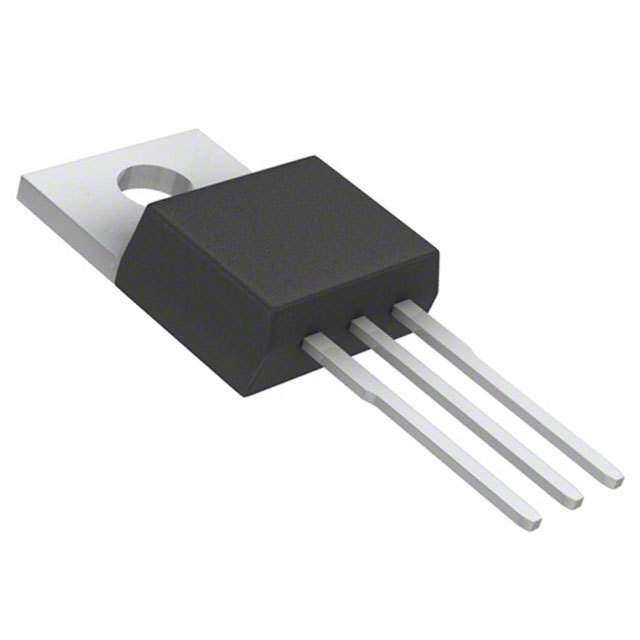
L79L Ordering information 6 Ordering information Table 14: Ordering information TO-92 TO-92 TO-92 (tape Output SO-8 SOT-89 (bag) (Ammopak) and reel) voltage (V) L79L05ABZ- L79L05ABD13TR L79L05ACZ L79L05ABUTR -5 AP L79L08ACZ- L79L05ACD13TR L79L05ACZ-TR L79L05ACUTR -5 AP L79L08ACD13TR -8 L79L12ACD13TR L79L12ACZ-TR L79L12ACUTR -12 L79L15ABD13TR -15 L79L15ACD13TR L79L15ACUTR -15 DocID2511 Rev 19 21/23
Revision history L79L 7 Revision history Table 15: Document revision history Date Revision Changes 14-Mar-2005 9 Add Tape and Reel for TO-92. 15-Mar-2005 10 Add note on Table 3. 23-Dec-2005 11 Mistake on ordering Table in Header. 12-Sep-2006 12 Order codes updated. 25-Jul-2007 13 Pin connection for SOT-89 updated on Figure 2. 04-Dec-2007 14 Modified: Table 14. 14-Jul-2008 15 Modified: Table 14 on page 24. 29-Jul-2009 16 Modified: Table 14 on page 24. Part numbers L79LxxAB, L78LxxAC, L78LxxC changed to L79L. Removed Table 1: Device summary. Updated the features and description in cover page. 17-Apr-2014 17 Updated Figure 1: Schematic diagram, Table 1: Absolute maximum ratings and Table 14: Order codes. Added Section 5: Packaging mechanical data. Minor text changes. Updated Section 5: Package information. 12-Feb-2016 18 Minor text changes. 06-Dec-2017 19 Updated features in cover page. 22/23 DocID2511 Rev 19
L79L IMPORTANT NOTICE – PLEASE READ CAREFULLY STMicroelectronics NV and its subsidiaries (“ST”) reserve the right to make changes, corrections, enhancements, modifications, and improvements to ST products and/or to this document at any time without notice. Purchasers should obtain the latest relevant information on ST products before placing orders. ST products are sold pursuant to ST’s terms and conditions of sale in place at the time of order acknowledgement. Purchasers are solely responsible for the choice, selection, and use of ST products and ST assumes no liability for application assistance or the design of Purchasers’ products. No license, express or implied, to any intellectual property right is granted by ST herein. Resale of ST products with provisions different from the information set forth herein shall void any warranty granted by ST for such product. ST and the ST logo are trademarks of ST. All other product or service names are the property of their respective owners. Information in this document supersedes and replaces information previously supplied in any prior versions of this document. © 2017 STMicroelectronics – All rights reserved DocID2511 Rev 19 23/23