ICGOO在线商城 > 集成电路(IC) > PMIC - 栅极驱动器 > L6569
 Datasheet下载
- 型号: L6569
- 制造商: STMicroelectronics
- 库位|库存: xxxx|xxxx
- 要求:
| 数量阶梯 | 香港交货 | 国内含税 |
| +xxxx | $xxxx | ¥xxxx |
查看当月历史价格
查看今年历史价格
L6569产品简介:
ICGOO电子元器件商城为您提供L6569由STMicroelectronics设计生产,在icgoo商城现货销售,并且可以通过原厂、代理商等渠道进行代购。 L6569价格参考¥询价-¥询价。STMicroelectronicsL6569封装/规格:PMIC - 栅极驱动器, Half-Bridge Gate Driver IC RC Input Circuit 8-Mini DIP。您可以下载L6569参考资料、Datasheet数据手册功能说明书,资料中有L6569 详细功能的应用电路图电压和使用方法及教程。
| 参数 | 数值 |
| 产品目录 | 集成电路 (IC)半导体 |
| 描述 | IC DRVR HALF BRDG HV W/OSC 8DIP门驱动器 Hi-Volt Half Bridge |
| 产品分类 | PMIC - MOSFET,电桥驱动器 - 外部开关集成电路 - IC |
| 品牌 | STMicroelectronics |
| 产品手册 | |
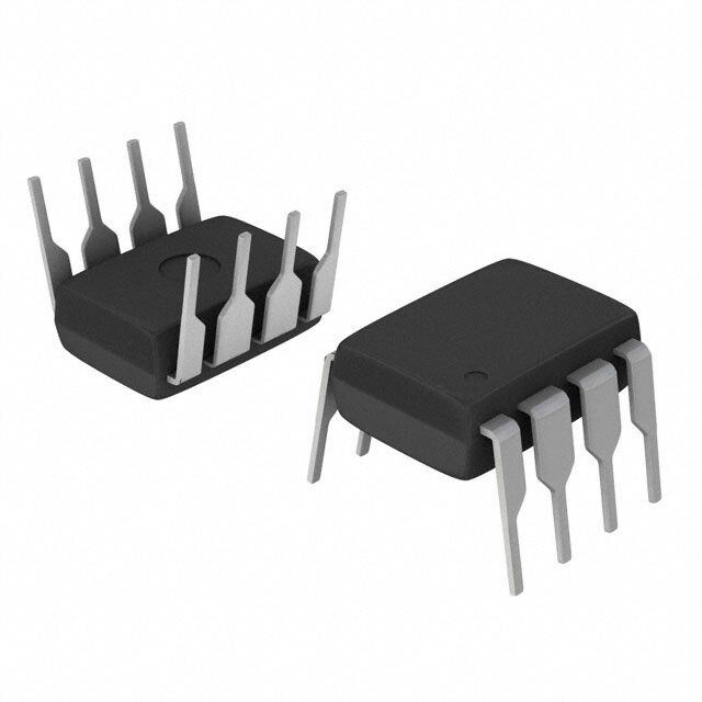
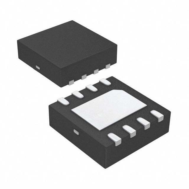
| 产品图片 |
|
| rohs | 符合RoHS无铅 / 符合限制有害物质指令(RoHS)规范要求 |
| 产品系列 | 电源管理 IC,门驱动器,STMicroelectronics L6569- |
| 数据手册 | |
| 产品型号 | L6569 |
| 产品目录页面 | |
| 产品种类 | 门驱动器 |
| 供应商器件封装 | 8-迷你型 DIP |
| 其它名称 | 497-4217-5 |
| 其它有关文件 | http://www.st.com/web/catalog/sense_power/FM142/CL1428/SC334/PF75504?referrer=70071840 |
| 包装 | 管件 |
| 商标 | STMicroelectronics |
| 安装类型 | 通孔 |
| 安装风格 | Through Hole |
| 封装 | Tube |
| 封装/外壳 | 8-DIP(0.300",7.62mm) |
| 封装/箱体 | PDIP-8 |
| 工作温度 | -40°C ~ 125°C |
| 工厂包装数量 | 50 |
| 延迟时间 | - |
| 最大工作温度 | + 125 C |
| 最小工作温度 | - 40 C |
| 标准包装 | 50 |
| 激励器数量 | 2 Driver |
| 电压-电源 | 10 V ~ 16.6 V |
| 电流-峰值 | 175mA |
| 电源电压-最小 | 10 V |
| 电源电流 | 25 mA |
| 类型 | High Voltage Half Bridge |
| 系列 | L6569 |
| 输入类型 | 自振荡 |
| 输出数 | 2 |
| 输出端数量 | 2 |
| 配用 | /product-detail/zh/STEVAL-ILB001V2/497-6409-ND/1786206/product-detail/zh/EVAL6569/497-4738-ND/954035 |
| 配置 | Self-Oscillating |
| 配置数 | 1 |
| 高压侧电压-最大值(自举) | 600V |


- 商务部:美国ITC正式对集成电路等产品启动337调查
- 曝三星4nm工艺存在良率问题 高通将骁龙8 Gen1或转产台积电
- 太阳诱电将投资9.5亿元在常州建新厂生产MLCC 预计2023年完工
- 英特尔发布欧洲新工厂建设计划 深化IDM 2.0 战略
- 台积电先进制程称霸业界 有大客户加持明年业绩稳了
- 达到5530亿美元!SIA预计今年全球半导体销售额将创下新高
- 英特尔拟将自动驾驶子公司Mobileye上市 估值或超500亿美元
- 三星加码芯片和SET,合并消费电子和移动部门,撤换高东真等 CEO
- 三星电子宣布重大人事变动 还合并消费电子和移动部门
- 海关总署:前11个月进口集成电路产品价值2.52万亿元 增长14.8%


PDF Datasheet 数据手册内容提取
L6569 L6569A HIGH VOLTAGE HALF BRIDGE DRIVER WITH OSCILLATOR n HIGH VOLTAGE RAIL UP TO 600V n BCD OFF LINE TECHNOLOGY n INTERNAL BOOTSTRAP DIODE STRUCTURE n 15.6V ZENER CLAMP ON VS n DRIVER CURRENT CAPABILITY: - SINK CURRENT = 270mA Minidip SO8 - SOURCE CURRENT = 170mA n VERY LOW START UP CURRENT: 150m A ORDERING NUMBERS: L6569 L6569D n UNDER VOLTAGE LOCKOUT WITH L6569A L6569AD HYSTERESIS n PROGRAMMABLE OSCILLATOR FREQUENCY be programmed using external resistor and capaci- n DEAD TIME 1.25m s tor. The internal circuitry of the device allows it to be driven also by external logic signal. n dV/dt IMMUNITY UP TO ±50V/ns The output drivers are designed to drive external n- n ESD PROTECTION channel power MOSFET and IGBT. The internal log- ic assures a dead time [typ. 1.25m s] to avoid cross- DESCRIPTION conduction of the power devices. The device is a high voltage half bridge driver with Two version are available: L6569 and L6569A. They built in oscillator. The frequency of the oscillator can differ in the low voltage gate driver start up sequence. BLOCK DIAGRAM H.V. CVS VS RHV BOOT 1 8 Source CHARGE PUMP BIAS LEVEL 7 HVG C BOOT REGULATOR SHIFTER V S HIGH SIDE RF 2 BUFFER DRIVER 6 OUT LOAD R F CF 3 COMP V S C LOW SIDE F DRIVER COMP LOGIC LVG GND 4 5 D94IN058D June 2000 1/13 This is preliminary information on a new product now in development. Details are subject to change without notice.
L6569 L6569A ABSOLUTE MAXIMUM RATINGS Symbol Parameter Value Unit IS (*) Supply Current 25 mA VCF Oscillator Resistor Voltage 18 V VLVG Low Side Switch Gate Output 14.6 V VOUT High Side Switch Source Output -1 to VBOOT - 18 V VHVG High Side Switch Gate Output -1 to VBOOT V VBOOT Floating Supply Voltage 618 V VBOOT/OUT Floating Supply vs OUT Voltage 18 V dVBOOT/dt VBOOT Slew Rate (Repetitive) – 50 V/ns dVOUT/dt VOUT Slew Rate (Repetitive) ± 50 V/ns Tstg Storage Temperature -40 to 150 °C Tj Junction Temperature -40 to 150 °C Tamb Ambient Temperature (Operative) -40 to 125 °C (*)The device has an internal zener clamp between GND and VS (typical 15.6V).Therefore the circuit should not be driven by a DC low im- pedance power source. Note: ESD immunity for pins 6, 7 and 8 is guaranteed up to 900 V (Human Body Model) THERMAL DATA Symbol Parameter Minidip SO8 Unit Rth j-amb Thermal Resistance Junction-Ambient Max 100 150 °C/W RECOMMENDED OPERATING CONDITIONS Symbol Parameter Min. Max. Unit VS Supply Voltage 10 VCL V VBOOT Floating Supply Voltage - 500 V VOUT High Side Switch Source Output -1 VBOOT -VCL V fout Oscillation Frequency 200 kHz PIN CONNECTION V 1 8 BOOT S RF 2 7 HVG C 3 6 OUT F GND 4 5 LVG D94IN059 2/13
L6569 L6569A PIN FUNCTION N° Pin Description 1 VS Supply input voltage with internal clamp [typ. 15.6V] 2 RF Oscillator timing resistor pin. A buffer set alternatively to VS and GND can provide current to the external resistor RF connected between pin 2 and 3. Alternatively, the signal on pin 2 can be used also to drive another IC (i.e. another L6569 to drive a full H-bridge) 3 CF Oscillator timing capacitor pin. A capacitor connected between this pin and GND fixes (together with RF) the oscillating frequency Alternatively an external logic signal can be applied to the pin to drive the IC. 4 GND Ground 5 LVG Low side driver output. The output stage can deliver 170mA source and 270mA sink [typ.values]. 6 OUT Upper driver floating reference 7 HVG High side driver output. The output stage can deliver 170mA source and 270mA sink [typ.values]. 8 BOOT Bootstrap voltage supply. It is the upper driver floating supply. The bootstrap capacitor connected between this pin and pin 6 can be fed by an internal structure named “bootstrap driver” (a patented structure). This structure can replace the external bootstrap diode. ELECTRICAL CHARACTERISTCS (VS = 12V; VBOOT - VOUT = 12V; Tj = 25°C; unless otherwise specified.) Symbol Pin Parameter Test Condition Min. Typ. Max. Unit VSUVP 1 VS Turn On Threshold 8.3 9 9.7 V VSUVN VS Turn Off Threshold 7.3 8 8.7 V VSUVH VS Hysteresis 0.7 1 1.3 V VCL VS Clamping Voltage IS = 5mA 14.6 15.6 16.6 V ISU Start Up Current VS < VSUVN 150 250 m A Iq Quiescent Current VS > VSUVP 500 700 m A IBOOTLK 8 Leakage Current BOOT pin vs VBOOT = 580V 5 m A GND IOUTLK 6 Leakage Current OUT pin vs VOUT = 562V 5 m A GND IHVG SO 7 High Side Driver Source Current VHVG = 6V 110 175 mA IHVG SI High Side Driver Sink Current VHVG = 6V 190 275 mA ILVG SO 5 Low Side Driver Source Current VLVG = 6V 110 175 mA ILVG SI Low Side Driver Sink Current VLVG = 6V 190 275 mA 3/13
L6569 L6569A ELECTRICAL CHARACTERISTCS (continued) Symbol Pin Parameter Test Condition Min. Typ. Max. Unit VRFON 2 RF High Level Output Voltage IRF = 1mA VS -0.05 VS -0.2 V VRF OFF RF Low Level Output Voltage IRF = -1mA 50 200 mV VCFU 3 CF Upper Threshold 7.7 8 8.2 V VCFL CF Lower Threshold 3.80 4 4.3 V td Internal Dead Time 0.85 1.25 1.65 m s DC Duty Cycle, Ratio Between Dead 0.45 0.5 0.55 Time + Conduction Time of High Side and Low Side Drivers RON On resistance of Boostrap 120 W LDMOS VBC Boostrap Voltage before UVLO VS = 8.2 2.5 3.6 V IAVE 1 Average Current from Vs No Load, fs = 60KHz 1.2 1.5 mA fout 6 Oscillation Frequency RT = 12K; CT = 1nF 57 60 63 kHz OSCILLATOR FREQUENCY The frequency of the internal oscillator can be programmed using external resistor and capacitor. The nominal oscillator frequency can be calculated using the following equation: 1 1 f = ----------------------------------------- = ------------------------------------------ OSC 2(cid:215) R (cid:215) C(cid:215) In2 1.3863(cid:215) R (cid:215) C F F F F Where RF and CF are the external resistor and capacitor. The device can be driven in "shut down" condition keeping the C pin close to GND, but some cares have to be F taken: 1. When CF is to GND the high side driver is off and the low side is on 2. The forced discharge of the oscillator capacitor CF must not be shorter than 1us: a simple way to do this is to limit the current discharge with a resistive path imposing R · CF >1m s (see fig.1) Figure 1. 1 8 2 7 R RF 3 6 fault signal CF 4 5 GNDM 4/13
L6569 L6569A Bootstrap Function The L6569 has an internal Bootstrap structure that enables the user to avoid the external diode needed, in sim- ilar devices, to perform the charge of the bootstrap capacitor that, in turns, provide an appropriate driving to the Upper External Mosfet. The operation is achieved with an unique structure (patented) that uses a High Voltage Lateral DMOS driven by an internal charge pump (see Block Diagram) and synchronized, with a 50 nsec delay, with the Low Side Gate driver (LVG pin), actually working as a synchronous rectifier . The charging path for the Bootstrap capacitor is closed via the Lower External Mosfet that is driven ON (i.e. LVG High) for a time interval: TC = RF · CF · In2 fi 1.1 · RF · CF starting from the time the Supply Voltage V has reached the Turn On Voltage (V = 9 V typical value). S SUVP After time T1 (see waveform Diagram) the LDMOS that charges the Bootstrap Capacitor, is on with a RON=120W (typical value). In the L6569A a different start up procedure is followed (see waveform Diagram). The Lower External Mosfet is drive OFF until VS has reached the Turn On Threshold (VSUVPp), then again the TC time interval starts as above. Being the LDMOS used to implement the bootstrap operation a "bi-directional" switch the current flowing into the BOOT pin (pin 8) can lead an undue stress to the LDMOS itself if a ZERO VOLTAGE SWITCHING opera- tions is not ensured, and then an high voltage is applied to the BOOT pin. This condition can occur, for example, when the load is removed and an high resistive value is placed in series with the gate of the external Power Mos. To help the user to secure his design a SAFE OPERATING AREA for the Bootstrap LDMOS is provided (fig. 7). Let's consider the steps that should be taken. 1) Calculate the Turn on delay ( td ) of your Lower Power MOS: t = (R +R )(cid:215) C (cid:215) ln ---------1----------- d g id iss V TH 1–----------- V S 2) Calculate the Fall time ( tf ) of your Lower Power MOS: R +R t = ------g--------------i-d---(cid:215) Q f V –V gd S TH where: Rg = External gate resistor R = 50W , typical equivalent output resistance of the driving buffer (when sourcing current) id VTH, Ciss and Qgd are Power MOS parameters V = Low Voltage Supply. S 3) Sketch the VBOOT waveform (using log-log scales) starting from the Drain Voltage of the Lower Power MOS (remember to add the Vs, your Low Voltage Supply, value) on the Bootstrap LDMOS SOA . On fig. 8 an example is given where: VS = Low Voltage Supply VHV = High Voltage Supply Rail The VBOOT voltage swing must fall below the curve identified by the actual operating frequency of your applica- tion. 5/13
L6569 L6569A DEMO BOARD To allow an easy evaluation of the device, a P.C. board dedicated to lamp ballast application has been de- signed. Fig.11 shows the electrical schematic of a typical ballast application, while the PC and component layout is giv- en in Fig12. This application has been designed to work with both the 110+/-20%V and the 220 +/- 20%V mains by means of a voltage doubler configuration at the bulk capacitor. The ballast inductance and the operating fre- quency are especially designed for a 18 W Sylvania De-luxe T/E type bulb. The PTC for preheat at the start up and the two back to back synchronization diodes, makes this application easy to implement and safe in opera- tion. part value R1 15ohm 1W R2, R3 22 ohm R4 27K R5 100K 1/2W R6 47ohm R7, R9 180K R8 120K 1/2W D1 18V zener D2, D3 BYW100-100 D4,D5,D6,D7 1N4007 D8 1N4148 C1 560pF 50V C2, C5 47m F 250V C3 4.7m F 25V C4 100nF 50V C6 100nF 250V C7-C8 8.2nF 630V C9 470pF 630V RV1 PTC 150ohm Q1, Q2 STD2NB50-1 L1 2.4mH 6/13
L6569 L6569A Figure 2. Waveforms (L6569) VS VSUVP VBOOT-VOUT VS 4.6V(typ) t=Ron*CBOOT VCF LVG T1 D95IN250B TC Figure 3. Waveforms (L6569A) VS VSUVP VBOOT-VOUT VS 4.6V(typ) t=Ron*CBOOT VCF LVG T1 D95IN251B TC 7/13
L6569 L6569A Figure 4. Typical Dead Time vs. Temperature Figure 7. Vboot pin SOA for different Operating Dependency Frequency @ Tj = 125°C Dead time [m sec] VBOOT 1.7 D96IN378A (V) D96IN381 500 110KHz 1.6 70KHz 300 1.5 50KHz 200 1.4 20KHz 100 1.3 1.2 50 1.1 30 150KHz 1 20 0.9 -50 0 50 100 150 10 20 50 100 200 500 1,000 2,000 5,000 10,000 Temperature [C] Time (ns), from LVG Transition High Figure 5. Typical Frequency vs Temperature Figure 8. V pin SOA @ T = 125°C boot j Dependency VBOOT Frequency [KHz] (V) D96IN416 65 D96IN379A 500 64 300 VHV+VS 63 200 62 ACTUAL OPERTATING FREQUENCY 61 100 60 50 59 VBOOT 58 30 57 20 td tf 56 VS 10 55 20 50 100 200 500 1,000 2,000 5,000 10,000 -50 -25 0 25 50 75 100 125 Time (ns), from LVG Transition High Temperature [C] Figure 9. Typical Rise and Fall Times vs. Load Figure 6. Typical and Theoretical Oscillator Capacitance Frequency vs Resistor Value time [nsec] f (KHz) 300 D96IN417 150 D96IN380 Theoretical 250 100 Tr 90 C=330pF 200 80 C=560pF 70 C=1nF 60 150 50 Tf 100 30 50 20 0 0 1 2 3 4 5 6 C [nF] 5 6 7 8 910 15 20 30 40 50 For both high and low side buffers @25˚C Tamb Resistor Value (Kohm) 8/13
L6569 L6569A Figure 10. Quiescent Current vs. Supply Voltage. Iq (m A) D96IN418 104 103 102 10 0 2 4 6 8 10 12 14 VS(V) Figure 11. CFL Demoboard 110/220V Inputs. Q1 R9 1R208K C2 VS BOOTC4100nF 50V STD2NB50-1 118/40WK 1/2W 24570mVF RF HVG R10 10K 4 x 1N4006 2R74K L6569 OUT R2 22 1/4W 1/4W L1=2.4mH D7 D4 1/4W CF R5 100K LVG R3 22 1/4W Q2 C7 2121N00VVR1 15 D1W6 D5 24C570m5VF 412./C7253mWVF 1ND4D81148 556C001VpRF6 47 1/4WC9 470pF 63G0NVD BSYTDW21N0B0-511100R8/-40107WK 120C5006nVF 8866..C3322008nnVVFF PT3RC5V0 11V50 ZPD 18V D2 CFL LAMP L1=2.4mH core TH LCC E2006-B4 Ref also VOGH 575 0409200 2.4mH D96IN419B D3 BYW100-100 SYLVANIA DELUX T/E 18W C7-C8=PS8n2J H3 630-2A TH 9/13
L6569 L6569A Figure 12. PC Board and Components Layout. Component Side Copper Side 10/13
L6569 L6569A mm inch DIM. OUTLINE AND MIN. TYP. MAX. MIN. TYP. MAX. MECHANICAL DATA A 1.75 0.069 a1 0.1 0.25 0.004 0.010 a2 1.65 0.065 a3 0.65 0.85 0.026 0.033 b 0.35 0.48 0.014 0.019 b1 0.19 0.25 0.007 0.010 C 0.25 0.5 0.010 0.020 c1 45(cid:176) (typ.) D (1) 4.8 5.0 0.189 0.197 E 5.8 6.2 0.228 0.244 e 1.27 0.050 e3 3.81 0.150 F (1) 3.8 4.0 0.15 0.157 L 0.4 1.27 0.016 0.050 SO8 M 0.6 0.024 S 8(cid:176) (max.) (1) D and F do not include mold flash or protrusions. Mold flash or potrusions shall not exceed 0.15mm (.006inch). 11/13
L6569 L6569A mm inch DIM. OUTLINE AND MIN. TYP. MAX. MIN. TYP. MAX. MECHANICAL DATA A 3.32 0.131 a1 0.51 0.020 B 1.15 1.65 0.045 0.065 b 0.356 0.55 0.014 0.022 b1 0.204 0.304 0.008 0.012 D 10.92 0.430 E 7.95 9.75 0.313 0.384 e 2.54 0.100 e3 7.62 0.300 e4 7.62 0.300 F 6.6 0.260 I 5.08 0.200 L 3.18 3.81 0.125 0.150 Minidip Z 1.52 0.060 12/13
L6569 L6569A Information furnished is believed to be accurate and reliable. However, STMicroelectronics assumes no responsibility for the consequences of use of such information nor for any infringement of patents or other rights of third parties which may result from its use. No license is granted by implication or otherwise under any patent or patent rights of STMicroelectronics. Specifications mentioned in this publication are subject to change without notice. This publication supersedes and replaces all information previously supplied. STMicroelectronics products are not authorized for use as critical components in life support devices or systems without express written approval of STMicroelectronics. The ST logo is a registered trademark of STMicroelectronics (cid:226) 2000 STMicroelectronics - All Rights Reserved STMicroelectronics GROUP OF COMPANIES Australia - Brazil - China - Finland - France - Germany - Hong Kong - India - Italy - Japan - Malaysia - Malta - Morocco - Singapore - Spain - Sweden - Switzerland - United Kingdom - U.S.A. http://www.st.com 13/13
Mouser Electronics Authorized Distributor Click to View Pricing, Inventory, Delivery & Lifecycle Information: S TMicroelectronics: L6569A L6569D L6569AD L6569 E-L6569D013TR L6569AD013TR L6569D013TR E-L6569D E-L6569