/KSZ8997.jpg)
 Datasheet下载
- 型号: KSZ8997
- 制造商: Micrel
- 库位|库存: xxxx|xxxx
- 要求:
| 数量阶梯 | 香港交货 | 国内含税 |
| +xxxx | $xxxx | ¥xxxx |
查看当月历史价格
查看今年历史价格
KSZ8997产品简介:
ICGOO电子元器件商城为您提供KSZ8997由Micrel设计生产,在icgoo商城现货销售,并且可以通过原厂、代理商等渠道进行代购。 KSZ8997价格参考。MicrelKSZ8997封装/规格:专用 IC, 10/100 Integrated Switch IC Port Switch/Network Interface 128-PQFP (14x20)。您可以下载KSZ8997参考资料、Datasheet数据手册功能说明书,资料中有KSZ8997 详细功能的应用电路图电压和使用方法及教程。
Microchip Technology的KSZ8997是一款专用集成电路(IC),主要用于以太网交换机应用。它属于非管理型千兆以太网三层交换机芯片,适用于需要高性能网络连接和数据传输的场景。

 应用场景

1. 企业网络:
   - KSZ8997广泛应用于中小型企业的局域网(LAN)中,提供稳定且高效的网络连接。它可以作为核心交换设备,支持多个终端设备的同时接入,确保数据传输的低延迟和高可靠性。

2. 工业自动化:
   - 在工业4.0背景下,KSZ8997可用于构建工厂内部的通信网络,实现生产设备之间的实时数据交换。其高可靠性和低功耗特性非常适合工业环境中的长时间稳定运行。

3. 智能建筑:
   - 智能建筑系统中,KSZ8997可以用于集成各种传感器、摄像头和其他智能设备的网络连接,确保楼宇自动化系统的高效运作。它支持PoE(以太网供电)功能,简化了布线复杂度,降低了安装成本。

4. 智能家居:
   - 在智能家居系统中,KSZ8997可以作为家庭网络的核心交换设备,连接智能家电、安防摄像头、智能音箱等设备,提供稳定的网络环境,支持高清视频流传输和远程控制功能。

5. 数据中心:
   - 数据中心对网络性能要求极高,KSZ8997可以用于构建内部交换网络,支持服务器之间的高速数据传输,提高数据处理效率。其三层路由功能使得网络拓扑更加灵活,便于管理和扩展。

6. 车载网络:
   - 随着汽车智能化的发展,KSZ8997也开始应用于车载以太网中,为自动驾驶、车内外通信提供高速、可靠的网络支持。它具备良好的电磁兼容性,适合严苛的车载环境。

 总结

KSZ8997凭借其高性能、低功耗和丰富的功能,在多种应用场景中展现出色的表现。无论是企业网络、工业自动化还是智能家居等领域,它都能提供稳定可靠的网络连接,满足不同用户的需求。
| 参数 | 数值 |
| 产品目录 | 集成电路 (IC)半导体 |
| 描述 | IC SWITCH 10/100 8PORT 128PQFP以太网 IC 8 Port 10/100 Switch with PHY and Frame Buffers (Lead Free) |
| 产品分类 | |
| 品牌 | Micrel |
| 产品手册 | |
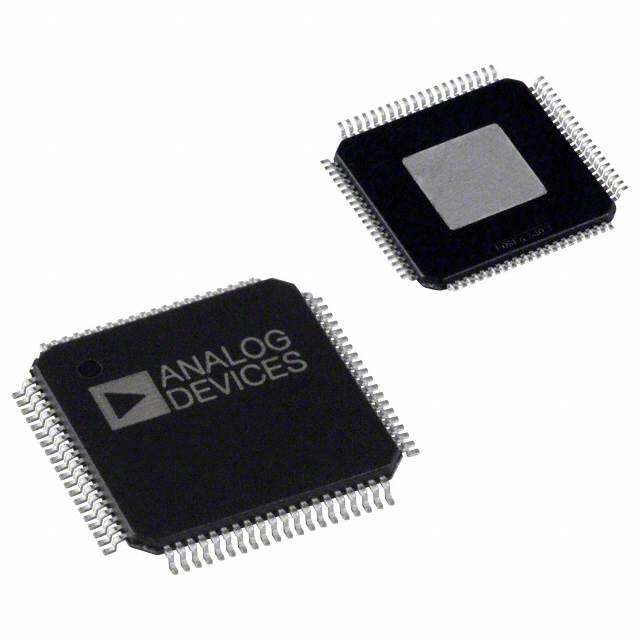
| 产品图片 |
|
| rohs | 符合RoHS无铅 / 符合限制有害物质指令(RoHS)规范要求 |
| 产品系列 | 通信及网络 IC,以太网 IC,Micrel KSZ8997- |
| 数据手册 | |
| 产品型号 | KSZ8997 |
| 产品 | Ethernet Switches |
| 产品目录页面 | |
| 产品种类 | 以太网 IC |
| 以太网连接类型 | 10Base-T, 100Base-TX |
| 供应商器件封装 | 128-PQFP(14x20) |
| 其它名称 | 576-1043 |
| 包装 | 托盘 |
| 商标 | Micrel |
| 安装类型 | 表面贴装 |
| 安装风格 | SMD/SMT |
| 封装 | Tray |
| 封装/外壳 | 128-BFQFP |
| 封装/箱体 | PQFP-128 |
| 工厂包装数量 | 66 |
| 应用 | 端口开关/网络接口 |
| 接口 | MII |
| 收发器数量 | 8 Transceiver |
| 数据速率 | 10 Mb/s, 100 Mb/s |
| 最大工作温度 | + 70 C |
| 最大电源电流 | 0.9 A |
| 最小工作温度 | 0 C |
| 标准包装 | 66 |
| 电源电压-最大 | 2.3 V |
| 电源电压-最小 | 2 V |
| 类型 | Integrated Switch |
| 系列 | KSZ8997 |


- 商务部:美国ITC正式对集成电路等产品启动337调查
- 曝三星4nm工艺存在良率问题 高通将骁龙8 Gen1或转产台积电
- 太阳诱电将投资9.5亿元在常州建新厂生产MLCC 预计2023年完工
- 英特尔发布欧洲新工厂建设计划 深化IDM 2.0 战略
- 台积电先进制程称霸业界 有大客户加持明年业绩稳了
- 达到5530亿美元!SIA预计今年全球半导体销售额将创下新高
- 英特尔拟将自动驾驶子公司Mobileye上市 估值或超500亿美元
- 三星加码芯片和SET,合并消费电子和移动部门,撤换高东真等 CEO
- 三星电子宣布重大人事变动 还合并消费电子和移动部门
- 海关总署:前11个月进口集成电路产品价值2.52万亿元 增长14.8%


PDF Datasheet 数据手册内容提取
KS8997/KSZ8997 8-Port 10/100 Integrated Switch with PHY and Frame Buffer Rev 1.1 General Description On the media side, the KS8997 supports 10BaseT and 100BaseTX through auto-negotiation as specified The KS8997 contains eight 10/100 physical layer by the IEEE 802.3 committee. transceivers, eight MAC (Media Access Control) units Physical signal transmission and reception are with an integrated layer 2 switch. The device runs as enhanced through use of analog circuitry that makes an eight port integrated switch. the design more efficient and allows for lower power The KS8997 is designed to reside in an unmanaged consumption and smaller chip die size. design not requiring processor intervention. This is Data sheets and support documentation can be found achieved through I/O strapping or EEPROM on Micrel’s web site at www.micrel.com. programming at system reset time. Functional Diagram Micrel Inc. • 2180 Fortune Drive • San Jose, CA 95131 • USA • tel +1 (408) 944-0800 • fax + 1 (408) 474-1000 • http://www.micrel.com February 2007 M9999-022807-1.31
Micrel, Inc. KS8997/KSZ8997 Features Applications • 8-port 10/100 integrated switch with 8 physical • Small workgroup switches layer transceivers • VoIP infrastructure switches • 32Kx32 of SRAM on chip for frame buffering Ordering Information • 2.0Gbps high performance memory bandwidth • 10BaseT and 100BaseTX modes of operation Part Number Temp. Range Package • Superior analog technology for reduced power and KS8997 0°C to +70°C 128-Pin PQFP die size • Single 2.0V power supply with options for 2.5V and KSZ8997 0°C to +70°C 128-Pin PQFP 3.3V I/O • 900mA (1.80 W) including physical transmit drivers • Supports port based VLAN • Supports DiffServ priority, 802.1p based priority or port based priority • Indicators for link, activity, full/half-duplex and speed • Unmanaged operation via strapping or EEPROM at system reset time • Hardware based 10/100, full/half, flow control and auto negotiation • Wire speed reception and transmission • Integrated address look-up engine, supports 1K absolute MAC addresses • Automatic address learning, address aging and address migration • Broadcast storm protection • Full-duplex IEEE 802.3x flow control • Half-duplex back pressure flow control • Comprehensive LED support • Supports MDI/MDI-X auto crossover • Commercial temperature range: 0°C to +70°C • Supports lead free product (KSZ8997) for commercial temperature range: 0°C to +70°C • Available in 128-pin PQFP package February 2007 2 M9999-022807-1.1
Micrel, Inc. KS8997/KSZ8997 Revision History Revision Date Summary of Changes 1.00 11/27/00 Document origination. 1.01 04/02/01 Update maximum frame size. Update EEPROM priority descriptions. Update I/O descriptions. Update Electrical Characteristics. 1.02 05/11/01 Add MDI/MDI_X description/ 1.03 06/22/01 Change electrical requirements. 1.04 06/25/01 Correct I/O descriptions. 1.05 07/25/01 Update PLL clock information. 1.06 05/29/02 Correct LED[1:8][3] mode 2 description. 1.07 08/29/03 Convert to new format. 1.1 02/27/07 Added lead free commercial temperature package. February 2007 3 M9999-022807-1.1
Micrel, Inc. KS8997/KSZ8997 Contents System Level Applications................................................................................................................................................6 Pin Description..................................................................................................................................................................7 I/O Grouping....................................................................................................................................................................11 I/O Descriptions...............................................................................................................................................................11 Pin Configuration.............................................................................................................................................................14 Functional Overview: Physical Layer Transceiver..........................................................................................................15 100BaseTX Transmit...................................................................................................................................................15 100BaseTX Receive....................................................................................................................................................15 PLL Clock Synthesizer................................................................................................................................................15 Scrambler/De-Scrambler (100BaseTX only)...............................................................................................................15 10BaseT Transmit.......................................................................................................................................................15 10BaseT Receive........................................................................................................................................................15 Power Management....................................................................................................................................................15 Power Save Mode..............................................................................................................................................15 MDI/MDI-X Auto Crossover.........................................................................................................................................16 Auto-Negotiation..........................................................................................................................................................16 Functional Overview: Switch Core..................................................................................................................................17 Address Look-Up.........................................................................................................................................................17 Learning.......................................................................................................................................................................17 Migration......................................................................................................................................................................17 Aging...........................................................................................................................................................................17 Forwarding...................................................................................................................................................................17 Switching Engine.........................................................................................................................................................17 MAC (Media Access Controller) Operation.................................................................................................................18 Inter-Packet Gap (IPG)......................................................................................................................................18 Backoff Algorithm...............................................................................................................................................18 Late Collision......................................................................................................................................................18 Illegal Frames.....................................................................................................................................................18 Flow Control.......................................................................................................................................................18 Half-Duplex Back Pressure................................................................................................................................18 Broadcast Storm Protection...............................................................................................................................18 Programmable Features.................................................................................................................................................19 Priority Schemes.........................................................................................................................................................19 Per Port Method..........................................................................................................................................................19 802.1p Method............................................................................................................................................................19 IPv4 DSCP Method.....................................................................................................................................................19 Other Priority Considerations......................................................................................................................................19 VLAN Operation..............................................................................................................................................................20 Station MAC Address (control frames only)....................................................................................................................21 EEPROM Operation........................................................................................................................................................21 EEPROM Memory Map...............................................................................................................................................21 General Control Register.............................................................................................................................................21 February 2007 4 M9999-022807-1.1
Micrel, Inc. KS8997/KSZ8997 Priority Classification Control – 802.1p tag field..........................................................................................................21 Port 1 Control Register................................................................................................................................................22 Port 2 Control Register................................................................................................................................................22 Port 3 Control Register................................................................................................................................................22 Port 4 Control Register................................................................................................................................................23 Port 5 Control Register................................................................................................................................................23 Port 6 Control Register................................................................................................................................................23 Port 7 Control Register................................................................................................................................................24 Port 8 Control Register................................................................................................................................................24 Reserved Register.......................................................................................................................................................25 Port 1 VLAN Mask Register........................................................................................................................................25 Port 2 VLAN Mask Register........................................................................................................................................25 Port 3 VLAN Mask Register........................................................................................................................................26 Port 4 VLAN Mask Register........................................................................................................................................26 Port 5 VLAN Mask Register........................................................................................................................................26 Port 6 VLAN Mask Register........................................................................................................................................27 Port 7 VLAN Mask Register........................................................................................................................................27 Port & VLAN Mask Register........................................................................................................................................28 Reserved Register.......................................................................................................................................................28 Port 1 VLAN Tag Insertion Value Registers................................................................................................................28 Port 2 VLAN Tag Insertion Value Registers................................................................................................................28 Port 3 VLAN Tag Insertion Value Registers................................................................................................................28 Port 4 VLAN Tag Insertion Value Registers................................................................................................................29 Port 5 VLAN Tag Insertion Value Registers................................................................................................................29 Port 6 VLAN Tag Insertion Value Registers................................................................................................................29 Port 7 VLAN Tag Insertion Value Registers................................................................................................................29 Port 8 VLAN Tag Insertion Value Registers................................................................................................................29 Reserved Register.......................................................................................................................................................29 Diff Serv Code Point Registers....................................................................................................................................29 Station MAC Address Registers (all ports – MAC control frames only)......................................................................30 Absolute Maximum Ratings............................................................................................................................................31 Operating Ratings...........................................................................................................................................................31 Electrical Characteristics.................................................................................................................................................31 Timing Diagrams.............................................................................................................................................................33 Reference Circuit.............................................................................................................................................................34 4B/5B Coding..................................................................................................................................................................35 MLT3 Coding...................................................................................................................................................................36 MAC Frame for 802.3......................................................................................................................................................36 Selection of Isolation Transformer..................................................................................................................................37 Selection of Reference Oscillator/Crystal........................................................................................................................37 Package Information.......................................................................................................................................................38 February 2007 5 M9999-022807-1.1
Micrel, Inc. KS8997/KSZ8997 System Level Applications The KS8997 can be configured to fit in an eight port unmanaged operation, flexible configuration, built in 10/100 application. The major benefits of using the frame buffering, VLAN abilities and traffic priority KS8997 are the lower power consumption, control. An application is depicted below. February 2007 6 M9999-022807-1.1
Micrel, Inc. KS8997/KSZ8997 Pin Description Pin Number Pin Name Type(1) Port Pin Function 1 VDD_RX Pwr 2.0V for equalizer 2 GND_RX Gnd Ground for equalizer 3 GND_RX Gnd Ground for equalizer 4 VDD_RX Pwr 2.0V for equalizer 5 RXP[3] I 3 Physical receive signal + (differential) 6 RXM[3] I 3 Physical receive signal – (differential) 7 GND-ISO Gnd Analog ground 8 TXP[3] O 3 Physical transmit signal + (differential) 9 TXM[3] O 3 Physical transmit signal – (differential) 10 GND_TX Gnd Ground for transmit circuitry 11 VDD_TX Pwr 2.0V for transmit circuitry 12 TXP[4] O 4 Physical receive signal + (differential) 13 TXM[4] O 4 Physical receive signal – (differential) 14 GND_TX Gnd Ground for transmit circuitry 15 RXP[4] I 4 Physical receive signal + (differential) 16 RXM[4] I 4 Physical receive signal – (differential) 17 GND_RX Gnd Ground for equalizer 18 VDD_RX Pwr 2.0V for equalizer 19 ISET Set physical transmit output current 20 GND-ISO Gnd Analog ground 21 VDD_RX Pwr 2.0V for equalizer 22 GND_RX Gnd Ground for equalizer 23 RXP[5] I 5 Physical receive signal + (differential) 24 RXM[5] I 5 Physical receive signal – (differential) 25 GND_TX Gnd Ground for transmit circuitry 26 TXP[5] O 5 Physical receive signal + (differential) 27 TXM[5] O 5 Physical receive signal – (differential) 28 VDD_TX Pwr 2.0V for transmit circuitry 29 GND_TX Gnd Ground for transmit circuitry 30 TXP[6] O 6 Physical receive signal + (differential) 31 TXM[6] O 6 Physical receive signal – (differential) 32 GND-ISO Gnd Analog ground 33 RXP[6] I 6 Physical receive signal + (differential) 34 RXM[6] I 6 Physical receive signal – (differential) 35 VDD_RX Pwr 2.0V for equalizer 36 GND_RX Gnd Ground for equalizer 37 GND_RX Gnd Ground for equalizer 38 VDD_RX Pwr 2.0V for equalizer February 2007 7 M9999-022807-1.1
Micrel, Inc. KS8997/KSZ8997 Pin Number Pin Name Type(1) Port Pin Function 39 GND-ISO Gnd Analog ground 40 RXP[7] I 7 Physical receive signal + (differential) 41 RXM[7] I 7 Physical receive signal - (differential) 42 GND_TX Gnd Ground for transmit circuitry 43 TXP[7] O 7 Physical receive signal + (differential) 44 TXM[7] O 7 Physical receive signal - (differential) 45 VDD_TX Pwr 2.0V for transmit circuitry 46 VDD_TX Pwr 2.0V for transmit circuitry 47 TXP[8] O 8 Physical receive signal + (differential) 48 TXM[8] O 8 Physical receive signal - (differential) 49 GND_TX Gnd Ground for transmit circuitry 50 RXP[8] I 8 Physical receive signal + (differential) 51 RXM[8] I 8 Physical receive signal - (differential) 52 GND_RX Gnd Ground for equalizer 53 VDD_RX Pwr 2.0V for equalizer 54 GND_RCV Gnd Ground for clock recovery circuit 55 VDD_RCV Pwr 2.0V for clock recovery circuit 56 GND_RCV Gnd Ground for clock recovery circuit 57 VDD_RCV Pwr 2.0V for clock recovery circuit 58 RLPBK I Enable loop back for testing 59 T[1] I Factory test pin – float for normal operation 60 EN1P I Enable 802.1p for all ports 61 SDA I/O Serial data from EEPROM or processor 62 SCL I/O Clock for EEPROM or from processor 63 VDD Pwr 2.0V for core digital circuitry 64 GND Gnd Ground for core digital circuitry 65 VDD-IO Pwr 2.0V, 2.5V or 3.3V for I/O circuitry 66 GND Gnd Ground for digital circuitry 67 GND Gnd Ground for core digital circuitry 68 VDD Pwr 2.0V for core digital circuitry 69 BIST I Built-in self test—tie low for normal operation 70 RST# I Reset 71 LED[1][3] I/O 1 LED indicator 3 72 LED[1][2] I/O 1 LED indicator 2 73 LED[1][0] I/O 1 LED indicator 0 74 LED[2][3] I/O 2 LED indicator 3 75 LED[2][2] I/O 2 LED indicator 2 76 LED[2][0] I/O 2 LED indicator 0 77 VDD-IO Pwr 2.0V, 2.5V or 3.3V for I/O circuitry February 2007 8 M9999-022807-1.1
Micrel, Inc. KS8997/KSZ8997 Pin Number Pin Name Type(1) Port Pin Function 78 GND Gnd Ground for digital circuitry 79 LED[3][3] I/O 3 LED indicator 3 80 LED[3][2] I/O 3 LED indicator 2 81 LED[3][0] I/O 3 LED indicator 0 82 LED[4][3] I/O 4 LED indicator 3 83 LED[4][2] I/O 4 LED indicator 2 84 LED[4][0] I/O 4 LED indicator 0 85 VDD Pwr 2.0V for core digital circuitry 86 GND Gnd Ground for core digital circuitry 87 LED[5][3] I/O 5 LED indicator 3 88 LED[5][2] I/O 5 LED indicator 2 89 LED[5][0] I/O 5 LED indicator 0 90 LED[6][3] I/O 6 LED indicator 3 91 LED[6][2] I/O 6 LED indicator 2 92 LED[6][0] I/O 6 LED indicator 0 93 LED[7][3] I/O 7 LED indicator 3 94 LED[7][2] I/O 7 LED indicator 2 95 VDD-IO Pwr 2.0V, 2.5V or 3.3V for I/O circuitry 96 LED[7][0] I/O 7 LED indicator 0 97 LED[8][3] I/O 8 LED indicator 3 98 LED[8][2] I/O 8 LED indicator 2 99 LED[8][0] I/O 8 LED indicator 0 100 GND Gnd Ground for digital circuitry 101 GND Gnd Ground for core digital circuitry 102 VDD Pwr 2.0V for core digital circuitry 103 MODESEL[1] I Selects LED modes 104 MODESEL[0] I Selects LED modes 105 T[5] I Factory test pin – float for normal operation 106 X1 I Crystal or clock input 107 X2 O Connect to crystal 108 VDD_PLLTX Pwr 2.0V for phase locked loop circuit 109 GND_PLLTX Gnd Ground for phase locked loop circuit 110 VDD_RCV Pwr 2.0V for clock recovery circuit 111 GND_RCV Gnd Ground for clock recovery circuit 112 VDD_RCV Pwr 2.0V for clock recovery circuit 113 GND_RCV Gnd Ground for clock recovery circuit 114 VDD_RX Pwr 2.0V for equalizer 115 GND_RX Gnd Ground for equalizer 116 RXP[1] I 1 Physical receive signal + (differential) February 2007 9 M9999-022807-1.1
Micrel, Inc. KS8997/KSZ8997 Pin Number Pin Name Type(1) Port Pin Function 117 RXM[1] I 1 Physical receive signal – (differential) 118 GND_TX Gnd Ground for transmit circuitry 119 TXP[1] O 1 Physical transmit signal + (differential) 120 TXM[1] O 1 Physical transmit signal - (differential) 121 VDD_TX Pwr 2.0V for transmit circuitry 122 VDD_TX Pwr 2.0V for transmit circuitry 123 TXP[2] O 2 Physical transmit signal + (differential) 124 TXM[2] O 2 Physical transmit signal - (differential) 125 GND_TX Gnd Ground for transmit circuitry 126 RXP[2] I 2 Physical transmit signal + (differential) 127 RXM[2] I 2 Physical transmit signal - (differential) 128 GND-ISO Gnd Analog ground Notes: 1. Pwr = Power supply I = Input O = Output I/O = Bi-directional Gnd = Ground February 2007 10 M9999-022807-1.1
Micrel, Inc. KS8997/KSZ8997 I/O Grouping Group Name Description PHY Physical interface IND LED Indicators UP Unmanaged Programmable CTRL Control and Miscellaneous TEST Test (Factory) PWR/GND Power and Ground I/O Descriptions Group I/O Names Active Status Description PHY RXP[1:8] Analog Differential inputs (receive) for connection to media transformer. RXM[1:8] IND TXP[1:8] Analog Differential outputs (transmit) for connection to media transformer. TXM[1:8] ISET Analog Transmit Current Set. Connect an external reference resistor to set transmitter output current. This pin is connected to a 1% 3kΩresistor to ground if a transformer with 1:1 turn ratio is used. LED[1:8][0] L Output (after reset) Mode 0: Speed (on = 100/off = 10) Mode 1: Reserve Mode 2: Collision (on = collision/off = no collision) Mode 3: Speed (on = 100/off = 10) LED[1:8][2] L Output (after reset) Mode 0: Collision (on = collision/off = no collision) Mode 1: Reserve Mode 2: Link Activity (10Mb mode) Mode 3: Full Duplex + Collision (constant on = full-duplex; intermittent on = collision; off = half-duplex with no collision) LED[1:8][3] L Output (after reset) Mode 0: Link + Activity Mode 1: Reserve Mode 2: Link Activity (100Mb mode) Mode 3: Link + Activity Note: Mode is set by MODESEL[1:0] ; See description in UP (unmanaged programming) section UP MODESEL[1:0] H Mode select at reset time. LED mode is selected by using the table below. MODESEL [1] [0] Operation 0 0 LED mode 0 0 1 LED mode 1 1 0 LED mode 2 1 1 LED mode 3 LED[1][3] Reserved – use float configuration LED[1][2] Reserved – use float configuration LED[1][0] Reserved – use float configuration LED[2][3] Reserved – use float configuration LED[2][2] Reserved – use float configuration February 2007 11 M9999-022807-1.1
Micrel, Inc. KS8997/KSZ8997 Group I/O Names Active Status Description LED[2][0] Reserved – use float configuration LED[3][3] Reserved – use float configuration LED[3][2] Reserved – use float configuration LED[3][0] Reserved – use float configuration LED[4][3] Reserved – use float configuration LED[4][2] Reserved – use float configuration LED[4][0] Reserved – use float configuration LED[5][3] Reserved – use float configuration LED[5][2] Reserved – use float configuration LED[5][0] Reserved – use float configuration LED[6][3] Programs back-off aggressiveness for half-duplex mode. D = Less aggressive back-off F/U = More aggressive back-off (default LED[6][2] Programs retries for frames that encounter collisions. LED[6][0] Reserved – use float configuration Programs flow control. LED[7][3] D = No flow control F/U = Flow control enabled (default) Programs broadcast storm protection. LED[7][2] D = 5% broadcast frames allowed F/U = Unlimited broadcast frames (default) LED[7][0] Reserved – use float configuration LED[8][3] Programs address aging. D = Aging disabled F/U = Enable 5 minute aging (default) LED[8][2] Programs frame length enforcement. D = Max length for VLAN is 1522 bytes and without VLAN is 1518 bytes F/U = Max length is 1536 bytes (default) LED[8][0] Programs half-duplex back pressure. D = No half-duplex back pressure F/U = Half-suplex back pressure enabled (default) CTRL EN1P H Enable 802.1p for all ports: this enables QoS based on the priority field in the layer 2 header. 0 = 802.1p selected by port in EEPROM 1 = Use 802.1p priority field unless disabled in EEPROM Note: This is also controlled by the EEPROM registers (registers 4-11 bit 4). The values in the EEPROM supercede this pin. Also, if the priority selection is unaltered in the EEPROM registers (register 3 bits 0-7) then values of ‘100’ and above are considered high priority and values of ‘011’ and below are low priority. X1 Clock External crystal or clock input X2 Used when other polarity of crystal is needed. This is unused for a normal Clock clock input. SCL Clock Clock for EEPROM. SDA Serial data for EEPROM. RST# L System reset. TEST T[1], T[5] Factory test inputs: leave open (float) for normal operation RLPBK H Factory test input: tie low for normal operation February 2007 12 M9999-022807-1.1
Micrel, Inc. KS8997/KSZ8997 Group I/O Names Active Status Description BIST H Factory test input: tie low for normal operation PWR/GND VDD_RX 2.0V for equalizer GND_RX Ground for equalizer VDD_TX 2.0V for transmit circuitry GND_TX Ground for transmit circuitry VDD_RCV 2.0V for clock recovery circuitry GND_RCV Ground for clock recovery VDD_PLLTX 2.0V for phase locked loop circuitry GND_PLLTX Ground for phase locked loop circuitry GND-SIO Analog ground VDD 2.0V for core digital circuitry VDD-IO 2.0V, 2.5V or 3.3V digital for I/O circuitry GND Ground for digital circuitry Note: 1. All unmanaged programming takes place at reset time only. For unmanaged programming: F = Float, D = Pull-down, U = Pull-up, H = Hold pin state after reset. See “Reference Circuits” section. February 2007 13 M9999-022807-1.1
Micrel, Inc. KS8997/KSZ8997 Pin Configuration 128-Pin PQFP (Q) February 2007 14 M9999-022807-1.1
Micrel, Inc. KS8997/KSZ8997 Functional Overview: Physical Layer Transceiver 100BaseTX Transmit The 100BaseTX transmit function performs parallel-to-serial conversion, 4B/5B coding, scrambling, NRZ to NRZI conversion, MLT3 encoding and transmission. The circuit starts with a parallel to serial conversion, which converts the MII data from the MAC into a 125MHz serial bit stream. The data and control stream is then converted into 4B/5B coding followed by a scrambler. The serialized data is further converted from NRZ to NRZI format, and then transmitted in MLT3 current output. The output current is set by an external 1% 3.01kΩ resistor for the 1:1 transformer ratio. It has a typical rise/fall time of 4ns and complies with the ANSI TP-PMD standard regarding amplitude balance, overshoot and timing jitter. The wave-shaped 10BaseT output is also incorporated into the 100BaseTX transmitter. 100BaseTX Receive The 100BaseTX receiver function performs adaptive equalization, DC restoration, MLT3 to NRZI conversion, data and clock recovery, NRZI to NRZ conversion, de-scrambling, 4B/5B decoding and serial to parallel conversion. The receiving side starts with the equalization filter to compensate for inter-symbol interference (ISI) over the twisted pair cable. Since the amplitude loss and phase distortion is a function of the length of the cable, the equalizer has to adjust its characteristics to optimize the performance. In this design, the variable equalizer will make an initial estimation based on comparisons of incoming signal strength against some known cable characteristics, then it tunes itself for optimization. This is an ongoing process and can self adjust against environmental changes such as temperature variations. The equalized signal then goes through a DC restoration and data conversion block. The DC restoration circuit is used to compensate for the effect of base line wander and improve the dynamic range. The differential data conversion circuit converts the MLT3 format back to NRZI. The slicing threshold is also adaptive. The clock recovery circuit extracts the 125MHz clock from the edges of the NRZI signal. This recovered clock is then used to convert the NRZI signal into the NRZ format. The signal is then sent through the de-scrambler followed by the 4B/5B decoder. Finally, the NRZ serial data is converted to the MII format and provided as the input data to the MAC. PLL Clock Synthesizer The KS8997 generates 125MHz, 62MHz, 25MHz and 10MHz clocks for system timing. Internal clocks are generated from an external 25MHz crystal. Scrambler/De-Scrambler (100BaseTX only) The purpose of the scrambler is to spread the power spectrum of the signal in order to reduce EMI and baseline wander. The data is scrambled through the use of an 11-bit wide linear feedback shift register (LFSR). This can generate a 2047-bit non-repetitive sequence. The receiver will then de-scramble the incoming data stream with the same sequence at the transmitter. 10BaseT Transmit The output 10BaseT driver is incorporated into the 100BaseT driver to allow transmission with the same magnetics. They are internally wave-shaped and pre-emphasized into outputs with a typical 2.3V amplitude. 10BaseT Receive On the receive side, input buffer and level detecting squelch circuits are employed. A differential input receiver circuit and a PLL perform the decoding function. The Manchester-encoded data stream is separated into clock signal and NRZ data. A squelch circuit rejects signals with levels less than 400mV or with short pulse widths in order to prevent noises at the RXP or RXM input from falsely triggering the decoder. When the input exceeds the squelch limit, the PLL locks onto the incoming signal and the KS8997 decodes a data frame. The receiver clock is maintained active during idle periods in between data reception. Power Management Power-Save Mode The KS8997 will turn off everything except for the Energy Detect and PLL circuits when the cable is not installed on an individual port basis. In other words, the KS8997 will shutdown most of the internal circuits to save power if there is no link. February 2007 15 M9999-022807-1.1
Micrel, Inc. KS8997/KSZ8997 MDI/MDI-X Auto Crossover The KS8997 supports MDI/MDI-X auto crossover. This facilitates the use of either a straight connection CAT-5 cable or a crossover CAT-5 cable. The auto-sense function will detect remote transmit and receive pairs, and correctly assign the transmit and receive pairs from the Micrel device. This can be highly useful when end users are unaware of cable types and can also save on an additional uplink configuration connection. The auto MDI/MDI-X is achieved by the Micrel device listening for the far end transmission channel and assigning transmit/receive pairs accordingly. Auto-Negotiation The KS8997 conforms to the auto-negotiation protocol as described by the 802.3 committee. Auto-negotiation allows UTP (Unshielded Twisted Pair) link partners to select the best common mode of operation. In auto-negotiation the link partners advertise capabilities across the link to each other. If auto-negotiation is not supported or the link partner to the KS8997 is forced to bypass auto-negotiation, then the mode is set by observing the signal at the receiver. This is known as parallel mode because while the transmitter is sending auto-negotiation advertisements, the receiver is listening for advertisements or a fixed signal protocol. The flow for the link set up is depicted below. Note that the KS8997 only supports auto-negotiation and not forced modes. Figure 4. Auto-Negotiation February 2007 16 M9999-022807-1.1
Micrel, Inc. KS8997/KSZ8997 Functional Overview: Switch Core Address Look-Up The internal look-up table stores MAC addresses and their associated information. It contains 1K full CAM with 48-bit address plus switching information. The KS8997 is guaranteed to learn 1K addresses and distinguishes itself from hash-based lookup tables which, depending on the operating environment and probabilities, may not guarantee the absolute number of addresses it can learn. Learning The internal look-up engine will update its table with a new entry if the following conditions are met: • The received packet’s SA (Source Address) does not exist in the look-up table. • The received packet is good; the packet has no receiving errors, and is of legal length. The look-up engine will insert the qualified SA into the table, along with the port number, time stamp. If the table is full, the last entry of the table will be deleted first to make room for the new entry. Migration The internal look-up engine also monitors whether a station is moved. If it happens, it will update the table accordingly. Migration happens when the following conditions are met: • The received packet’s SA is in the table but the associated source port information is different. • The received packet is good; the packet has no receiving errors, and is of legal length. The look-up engine will update the existing record in the table with the new source port information. Aging The look-up engine will update time stamp information of a record whenever the corresponding SA appears. The time stamp is used in the aging process. If a record is not updated for a period of time, the look-up engine will then remove the record from the table. The look-up engine constantly performs the aging process and will continuously remove aging records. The aging period is 300 seconds. This feature can be enabled or disabled by external pull-up or pull-down resistors. Forwarding The KS8997 will forward packets as follows: • If the DA look-up result is a “match”, the KS8997 will use the destination port information to determine where the packet goes. • If the DA look-up result is a “miss”, the KS8997 will forward the packet to all other ports except the port that received the packet. • All the multicast and broadcast packets will be forwarded to all other ports except the source port. The KS8997 will not forward the following packets: • Error packets. These include framing errors, FCS errors, alignment errors, and illegal size packet errors. • 802.3x pause frames. The KS8997 will intercept these packets and do the appropriate actions. • “Local” packets. Based on destination address (DA) look-up. If the destination port from the look-up table matches the port where the packet was from, the packet is defined as “local”. Switching Engine The KS8997 has a very high performance switching engine to move data to and from the MAC’s, packet buffers. It operates in store and forward mode, while the efficient switching mechanism reduces overall latency. The KS8997 has an internal buffer for frames that is 32Kx32 (128KB). This resource could be shared between the nine ports and is programmed at system reset time by using the unmanaged program mode (I/O strapping). Each buffer is sized at 128B and therefore there are a total of 1024 buffers available. The buffers are adaptively allocated up to 512 to a single port based on loading. February 2007 17 M9999-022807-1.1
Micrel, Inc. KS8997/KSZ8997 MAC (Media Access Controller) Operation The KS8995X strictly abides by IEEE 802.3 standards to maximize compatibility. Inter-Packet Gap (IPG) If a frame is successfully transmitted, the 96 bit time IPG is measured between the two consecutive MTXEN. If the current packet is experiencing collision, the 96 bit time IPG is measured from MCRS and the next MTXEN. Backoff Algorithm The KS8997 implements the IEEE Std 802.3 binary exponential back-off algorithm, and optional “aggressive mode” back off. After 16 collisions, the packet will be optionally dropped depending on the chip configuration in Register 3. See “Register 3.” Late Collision If a transmit packet experiences collisions after 512-bit times of the transmission, the packet will be dropped. Illegal Frames The KS8997 discards frames less than 64 bytes and can be programmed to accept frames up to 1536 bytes. Since the KS8997 supports VLAN tags, the maximum sizing is adjusted when these tags are present. Flow Control The KS8997 supports standard 802.3x flow control frames on both transmit and receive sides. On the receive side, if the KS8997 receives a pause control frame, the KS8997 will not transmit the next normal frame until the timer, specified in the pause control frame, expires. If another pause frame is received before the current timer expires, the timer will be updated with the new value in the second pause frame. During this period (being flow controlled), only flow control packets from the KS8997 will be transmitted. On the transmit side, the KS8997 has intelligent and efficient ways to determine when to invoke flow control. The flow control is based on availability of the system resources, including available buffers, available transmit queues and available receive queues. The KS8997 will flow control a port, which just received a packet, if the destination port resource is being used up. The KS8997 will issue a flow control frame (XOFF), containing the maximum pause time defined in IEEE standard 802.3x. Once the resource is freed up, the KS8997 will send out the other flow control frame (XON) with zero pause time to turn off the flow control (turn on transmission to the port). A hysteresis feature is provided to prevent flow control mechanism from being activated and deactivated too many times. The KS8997 will flow control all ports if the receive queue becomes full. Half-Duplex Back Pressure Half duplex back pressure option (Note: not in 802.3 standards) is also provided. The activation and deactivation conditions are the same as the above in full-duplex mode. If back pressure is required, the KS8997 will send preambles to defer other stations’ transmission (carrier sense deference). To avoid jabber and excessive deference defined in 802.3 standard, after a certain time it will discontinue the carrier sense but it will raise the carrier sense quickly. This short silent time (no carrier sense) is to prevent other stations from sending out packets and keeps other stations in carrier sense deferred state. If the port has packets to send during a back pressure situation, the carrier sense type back pressure will be interrupted and those packets will be transmitted instead. If there are no more packets to send, carrier sense type back pressure will be active again until switch resources free up. If a collision occurs, the binary exponential back-off algorithm is skipped and carrier sense is generated immediately, reducing the chance of further colliding and maintaining carrier sense to prevent reception of packets. Broadcast Storm Protection The KS8997 has an intelligent option to protect the switch system from receiving too many broadcast packets. Broadcast packets will be forwarded to all ports except the source port, and thus will use too many switch resources (bandwidth and available space in transmit queues). The KS8997 will discard broadcast packets if the number of those packets exceeds the threshold (configured by strapping during reset and EEPROM settings) in a preset period of time. If the preset period expires it will then resume receiving broadcast packets until the threshold is reached. The options are 5% of network line rate for the maximum broadcast receiving threshold or unlimited (feature off). February 2007 18 M9999-022807-1.1
Micrel, Inc. KS8997/KSZ8997 Programmable Features Priority Schemes The KS8997 can determine priority through three different means at the ingress point. The first method is a simple per port method, the second is via the 802.1p frame tag and the third is by viewing the DSCP (TOS) field in the IPv4 header. Of course for the priority to be effective, the high and low priority queues must be enabled on the destination port or egress point. Per Port Method General priority can be specified on a per port basis. In this type of priority all traffic from the specified input port is considered high priority in the destination queue. This can be useful in IP phone applications mixed with other data types of traffic where the IP phone connects to a specific port. The IP phone traffic would be high priority (outbound) to the wide area network. The inbound traffic to the IP phone is all of the same priority to the IP phone. 802.1p Method This method works well when used with ports that have mixed data and media flows. The inbound port examines the priority field in the tag and determines the high or low priority. Priority profiles are setup in the Priority Classification Control in the “EEPROM Memory Map” section. IPv4 DSCP Method This is another per frame way of determining outbound priority. The DSCP (Differentiated Services Code Point– RFC#2474) method uses the TOS field in the IP header to determine high and low priority on a per code point basis. Each fully decoded code point can have either a high or low priority. A larger spectrum of priority flows can be defined with this larger code space. More specific to implementation, the most significant 6 bits of the TOS field are fully decoded into 64 possibilities, and the singular code that results is compared against the corresponding bit in the DSCP register. If the register bit is a 1, the priority is high and if 0, the priority is low. Other Priority Considerations When setting up the priority scheme, one should consider other available controls to regulate the traffic. One of these is Priority Control Scheme (register 2 bits 2-3) which controls the interleaving of high and low priority frames. Options allow from a 2:1 ratio up to a setting that sends all the high priority first. This setting controls all ports globally. Another global feature is Priority Buffer Reserve (register 2 bit 1). If this is set, there is a 6KB (10%) buffer dedicated to high priority traffic, otherwise if cleared the buffer is shared between all traffic. On an individual port basis there are controls that enable DSCP, 802.1p, port based and high/low priority queues. These are contained in registers 4-11 bits 5-3 and 0. It should be noted that there is a special pin that generally enables the 802.1p priority for all ports (pin 60). When this pin is active (high) all ports will have the 802.1p priority enabled unless specifically disabled by EEPROM programming (bit 4 of registers 4-11). Default high priority is a value of '100' and above in the VLAN tag with low priority being a value of '011' and below. February 2007 19 M9999-022807-1.1
Micrel, Inc. KS8997/KSZ8997 The table below briefly summarizes priority features. For more detailed settings see “EEPROM Memory Map” section. Register(s) Bit(s) Global/Port Description General 2 3-2 Global Priority Control Scheme: Transmit buffer high/low interleave control 2 1 Global Priority Buffer Reserve: Reserves 6KB of the buffer for high priority traffic Enable Port Queue Split: Splits the transmit queue on the desired port for high 4-11 0 Port and low priority traffic DSCP Priority 4-11 5 Port Enable Port DSC: Looks at DSCP field in IP header to decide high or low priority DSCP Priority Points: Fully decoded 64-bit register used to determine priority 40-47 7-0 Global from DSCP field (6 bits) in the IP header 802.1p Priority 4-11 4 Port Enable Port 802.1p Priority: Uses the 802.1p priority tag (3 bits) to determine frame priority 3 7-0 Global Priority Classification: Determines which tag values have high priority Per Port Priority 4-11 3 Port Enable Port Priority: Determines which ports have high priority traffic Table 1. Priority Control VLAN Operation The VLAN’s are setup by programming the VLAN Mask Registers in the “EEPROM Memory Map” section. The perspective of the VLAN is from the input port and which output ports it sees directly through the switch. For example if port 1 only participated in a VLAN with ports 2 and 8 then one would set bits 0 and 6 in register 13 (Port 1 VLAN Mask Register). Note that different ports can be setup independently. An example of this would be where a router is connected to port 8 and each of the other ports would work autonomously. In this configuration ports 1 through 7 would only set the mask for port 8 and port 8 would set the mask for ports 1 through 7. In this way the router could see all ports and each of the other individual ports would only communicate with the router. All multicast and broadcast frames adhere to the VLAN configuration. Unicast frame treatment is a function of register 2 bit 0. If this bit is set then unicast frames only see ports within their VLAN. If this bit is cleared unicast frames can traverse VLAN’s. VLAN tags can be added or removed on a per port basis. Further, there are provisions to specify the tag value to be inserted on a per port basis. The table below briefly summarizes VLAN features. For more detailed settings see “EEPROM Memory Map” section. Register(s) Bit(s) Global/Port Description 4-11 2 Port Insert VLAN Tags: If specified, will add VLAN tags to frames without existing tags 4-11 1 Port Strip VLAN Tags: If specified, will remove VLAN tags from frames if they exist 2 0 Global VLAN Enforcement: Allows unicast frames to adhere or ignore the VLAN configuration 13-20 7-0 Port VLAN Mask Registers: Allows configuration of individual VLAN grouping VLAN Tag Insertion Values: Specifies the VLAN tag to be inserted if enabled (see 22-38 7-0 Port above) Table 2. VLAN Control February 2007 20 M9999-022807-1.1
Micrel, Inc. KS8997/KSZ8997 Station MAC Address (control frames only) The MAC source address can be programmed as used in flow control frames. The table below briefly summarizes this progammable feature. Register(s) Bit(s) Global/Port Description Station MAC Address: Used as source address for MAC control frames as used in 48-53 7-0 Global full-duplex flow control mechanisms. Table 3. Misc. Control EEPROM Operation The EEPROM interface utilizes 2 pins that provide a clock and a serial data path. As part of the initialization sequence, the KS8997 reads the contents of the EEPROM and loads the values into the appropriate registers. Note that the first two bytes in the EEPROM must be “55” and “99” respectively for the loading to occur properly. If these first two values are not correct, all other data will be ignored. Data start and stop conditions are signaled on the data line as a state transition during clock high time. A high to low transition indicates start of data and a low to high transition indicates a stop condition. The actual data that traverses the serial line changes during the clock low time. The KS8997 EEPROM interface is compatible with the Atmel AT24C01A part. Further timing and data sequences can be found in the Atmel AT24C01A specification. EEPROM Memory Map Default Address Name Description (chip) Value 0 7-0 Signature byte 1. Value = “55” 0x55 1 7-0 Signature byte 2. Value = “99” 0x99 General Control Register 2 7-4 Reserved – set to zero 0000 Priority control scheme (all ports) 00 = Transmit all high priority before any low priority 2 3-2 01 = Transmit high and low priority at a 10:1 ratio 00 10 = Transmit high and low priority at a 5:1 ratio 11 = Transmit high and low priority at a 2:1 ratio Priority buffer reserve for high priority traffic 2 1 1 = Reserve 6KB of buffer space for high priority 0 0 = None reserved VLAN enforcement 2 0 1 = All Unicast frames adhere to VLAN configuration 0 0 = Unicast frames ignore VLAN configuration Priority Classification Control – 802.1p tag field 1 = State “111” is high priority 3 7 1 0 = State “111” is low priority 1 = State “110” is high priority 3 6 1 0 = State “110” is low priority 1 = State “101” is high priority 3 5 1 0 = State “101” is low priority 1 = State “100” is high priority 3 4 1 0 = State “100” is low priority 1 = State “011” is high priority 3 3 0 0 = State “011” is low priority 1 = State “010” is high priority 3 2 0 0 = State “010” is low priority 3 1 1 = State “001” is high priority 0 February 2007 21 M9999-022807-1.1
Micrel, Inc. KS8997/KSZ8997 Default Address Name Description (chip) Value 0 = State “001” is low priority 1 = State “000” is high priority 3 0 0 0 = State “000” is low priority Port 1 Control Register 4 7-6 Reserved – set to zero 00 TOS priority classification enable for port 1 4 5 1 = Enable 0 0 = Disable 802.1p priority classification enable for port 1 4 4 1 = Enable 0 0 = Disable Port based priority classification for port 1 4 3 1 = High priority 0 0 = Low priority Insert VLAN tags for port 1 if non-existent 4 2 1 = Enable 0 0 = Disable Strip VLAN tags for port 1 if existent 4 1 1 = Enable 0 0 = Disable Enable high and low output priority queues for port 1 4 0 1 = Enable 0 0 = Disable Port 2 Control Register 5 7-6 Reserved – set to zero 00 TOS priority classification enable for port 2 5 5 1 = Enable 0 0 = Disable 802.1p priority classification enable for port 2 5 4 1 = Enable 0 0 = Disable Port based priority classification for port 2 5 3 1 = High priority 0 0 = Low priority Insert VLAN tags for port 2 if non-existent 5 2 1 = Enable 0 0 = Disable Strip VLAN tags for port 2 if existent 5 1 1 = Enable 0 0 = Disable Enable high and low output priority queues for port 2 5 0 1 = Enable 0 0 = Disable Port 3 Control Register 6 7-6 Reserved – set to zero 00 TOS priority classification enable for port 3 6 5 1 = Enable 0 0 = Disable 802.1p priority classification enable for port 3 6 4 1 = Enable 0 0 = Disable Port based priority classification for port 3 6 3 0 1 = High priority February 2007 22 M9999-022807-1.1
Micrel, Inc. KS8997/KSZ8997 Default Address Name Description (chip) Value 0 = Low priority Insert VLAN tags for port 3 if non-existent 6 2 1 = Enable 0 0 = Disable Strip VLAN tags for port 3 if existent 6 1 1 = Enable 0 0 = Disable Enable high and low output priority queues for port 3 6 0 1 = Enable 0 0 = Disable Port 4 Control Register 7 7-6 Reserved – set to zero 00 TOS priority classification enable for port 4 7 5 1 = Enable 0 0 = Disable 802.1p priority classification enable for port 4 7 4 1 = Enable 0 0 = Disable Port based priority classification for port 4 7 3 1 = High priority 0 0 = Low priority Insert VLAN tags for port 4 if non-existent 7 2 1 = Enable 0 0 = Disable Strip VLAN tags for port 4 if existent 7 1 1 = Enable 0 0 = Disable Enable high and low output priority queues for port 4 7 0 1 = Enable 0 0 = Disable Port 5 Control Register 8 7-6 Reserved – set to zero 00 TOS priority classification enable for port 5 8 5 1 = Enable 0 0 = Disable 802.1p priority classification enable for port 5 8 4 1 = Enable 0 0 = Disable Port based priority classification for port 5 8 3 1 = High priority 0 0 = Low priority Insert VLAN tags for port 5 if non-existent 8 2 1 = Enable 0 0 = Disable Strip VLAN tags for port 5 if existent 8 1 1 = Enable 0 0 = Disable Enable high and low output priority queues for port 5 8 0 1 = Enable 0 0 = Disable Port 6 Control Register 9 7-6 Reserved – set to zero 00 February 2007 23 M9999-022807-1.1
Micrel, Inc. KS8997/KSZ8997 Default Address Name Description (chip) Value TOS priority classification enable for port 6 9 5 1 = Enable 0 0 = Disable 802.1p priority classification enable for port 6 9 4 1 = Enable 0 0 = Disable Port based priority classification for port 6 9 3 1 = High priority 0 0 = Low priority Insert VLAN tags for port 6 if non-existent 9 2 1 = Enable 0 0 = Disable Strip VLAN tags for port 6 if existent 9 1 1 = Enable 0 0 = Disable Enable high and low output priority queues for port 6 9 0 1 = Enable 0 0 = Disable Port 7 Control Register 10 7-6 Reserved – set to zero 00 TOS priority classification enable for port 7 10 5 1 = Enable 0 0 = Disable 802.1p priority classification enable for port 7 10 4 1 = Enable 0 0 = Disable Port based priority classification for port 7 10 3 1 = High priority 0 0 = Low priority Insert VLAN tags for port 7 if non-existent 10 2 1 = Enable 0 0 = Disable Strip VLAN tags for port 7 if existent 10 1 1 = Enable 0 0 = Disable Enable high and low output priority queues for port 7 10 0 1 = Enable 0 0 = Disable Port 8 Control Register 11 7-6 Reserved – set to zero 00 TOS priority classification enable for port 8 11 5 1 = Enable 0 0 = Disable 802.1p priority classification enable for port 8 11 4 1 = Enable 0 0 = Disable Port based priority classification for port 8 11 3 1 = High priority 0 0 = Low priority Insert VLAN tags for port 8 if non-existent 11 2 1 = Enable 0 0 = Disable Strip VLAN tags for port 8 if existent 11 1 1 = Enable 0 0 = Disable February 2007 24 M9999-022807-1.1
Micrel, Inc. KS8997/KSZ8997 Default Address Name Description (chip) Value Enable high and low output priority queues for port 8 11 0 1 = Enable 0 0 = Disable Reserved Register 12 7-0 Reserved 0x00 Port 1 VLAN Mask Register 13 7 Reserved 1 Port 8 inclusion 13 6 1 = Port 8 in the same VLAN as port 1 1 0 = Port 8 not in the same VLAN as port 1 Port 7 inclusion 13 5 1 = Port 7 in the same VLAN as port 1 1 0 = Port 7 not in the same VLAN as port 1 Port 6 inclusion 13 4 1 = Port 6 in the same VLAN as port 1 1 0 = Port 6 not in the same VLAN as port 1 Port 5 inclusion 13 3 1 = Port 5 in the same VLAN as port 1 1 0 = Port 5 not in the same VLAN as port 1 Port 4 inclusion 13 2 1 = Port 4 in the same VLAN as port 1 1 0 = Port 4 not in the same VLAN as port 1 Port 3 inclusion 13 1 1 = Port 3 in the same VLAN as port 1 1 0 = Port 3 not in the same VLAN as port 1 Port 2 inclusion 13 0 1 = Port 2 in the same VLAN as port 1 1 0 = Port 2 not in the same VLAN as port 1 Port 2 VLAN Mask Register 14 7 Reserved 1 Port 8 inclusion 14 6 1 = Port 8 in the same VLAN as port 2 1 0 = Port 8 not in the same VLAN as port 2 Port 7 inclusion 14 5 1 = Port 7 in the same VLAN as port 2 1 0 = Port 7 not in the same VLAN as port 2 Port 6 inclusion 14 4 1 = Port 6 in the same VLAN as port 2 1 0 = Port 6 not in the same VLAN as port 2 Port 5 inclusion 14 3 1 = Port 5 in the same VLAN as port 2 1 0 = Port 5 not in the same VLAN as port 2 Port 4 inclusion 14 2 1 = Port 4 in the same VLAN as port 2 1 0 = Port 4 not in the same VLAN as port 2 Port 3 inclusion 14 1 1 = Port 3 in the same VLAN as port 2 1 0 = Port 3 not in the same VLAN as port 2 Port 2 inclusion 14 0 1 = Port 2 in the same VLAN as port 2 1 0 = Port 2 not in the same VLAN as port 2 February 2007 25 M9999-022807-1.1
Micrel, Inc. KS8997/KSZ8997 Default Address Name Description (chip) Value Port 3 VLAN Mask Register 15 7 Reserved 1 Port 8 inclusion 15 6 1 = Port 8 in the same VLAN as port 3 1 0 = Port 8 not in the same VLAN as port 3 Port 7 inclusion 15 5 1 = Port 7 in the same VLAN as port 3 1 0 = Port 7 not in the same VLAN as port 3 Port 6 inclusion 15 4 1 = Port 6 in the same VLAN as port 3 1 0 = Port 6 not in the same VLAN as port 3 Port 5 inclusion 15 3 1 = Port 5 in the same VLAN as port 3 1 0 = Port 5 not in the same VLAN as port 3 Port 4 inclusion 15 2 1 = Port 4 in the same VLAN as port 3 1 0 = Port 4 not in the same VLAN as port 3 Port 3 inclusion 15 1 1 = Port 3 in the same VLAN as port 3 1 0 = Port 3 not in the same VLAN as port 3 Port 2 inclusion 15 0 1 = Port 2 in the same VLAN as port 3 1 0 = Port 2 not in the same VLAN as port 3 Port 4 VLAN Mask Register 16 7 Reserved 1 Port 8 inclusion 16 6 1 = Port 8 in the same VLAN as port 4 1 0 = Port 8 not in the same VLAN as port 4 Port 7 inclusion 16 5 1 = Port 7 in the same VLAN as port 4 1 0 = Port 7 not in the same VLAN as port 4 Port 6 inclusion 16 4 1 = Port 6 in the same VLAN as port 4 1 0 = Port 6 not in the same VLAN as port 4 Port 5 inclusion 16 3 1 = Port 5 in the same VLAN as port 4 1 0 = Port 5 not in the same VLAN as port 4 Port 4 inclusion 16 2 1 = Port 4 in the same VLAN as port 4 1 0 = Port 4 not in the same VLAN as port 4 Port 3 inclusion 16 1 1 = Port 3 in the same VLAN as port 4 1 0 = Port 3 not in the same VLAN as port 4 Port 2 inclusion 16 0 1 = Port 2 in the same VLAN as port 4 1 0 = Port 2 not in the same VLAN as port 4 Port 5 VLAN Mask Register 17 7 Reserved 1 Port 8 inclusion 17 6 1 = Port 8 in the same VLAN as port 5 1 0 = Port 8 not in the same VLAN as port 5 Port 7 inclusion 17 5 1 = Port 7 in the same VLAN as port 5 1 0 = Port 7 not in the same VLAN as port 5 February 2007 26 M9999-022807-1.1
Micrel, Inc. KS8997/KSZ8997 Default Address Name Description (chip) Value Port 6 inclusion 17 4 1 = Port 6 in the same VLAN as port 5 1 0 = Port 6 not in the same VLAN as port 5 Port 5 inclusion 17 3 1 = Port 5 in the same VLAN as port 5 1 0 = Port 5 not in the same VLAN as port 5 Port 4 inclusion 17 2 1 = Port 4 in the same VLAN as port 5 1 0 = Port 4 not in the same VLAN as port 5 Port 3 inclusion 17 1 1 = Port 3 in the same VLAN as port 5 1 0 = Port 3 not in the same VLAN as port 5 Port 2 inclusion 17 0 1 = Port 2 in the same VLAN as port 5 1 0 = Port 2 not in the same VLAN as port 5 Port 6 VLAN Mask Register 18 7 Reserved 1 Port 8 inclusion 18 6 1 = Port 8 in the same VLAN as port 6 1 0 = Port 8 not in the same VLAN as port 6 Port 7 inclusion 18 5 1 = Port 7 in the same VLAN as port 6 1 0 = Port 7 not in the same VLAN as port 6 Port 6 inclusion 18 4 1 = Port 6 in the same VLAN as port 6 1 0 = Port 6 not in the same VLAN as port 6 Port 5 inclusion 18 3 1 = Port 5 in the same VLAN as port 6 1 0 = Port 5 not in the same VLAN as port 6 Port 4 inclusion 18 2 1 = Port 4 in the same VLAN as port 6 1 0 = Port 4 not in the same VLAN as port 6 Port 3 inclusion 18 1 1 = Port 3 in the same VLAN as port 6 1 0 = Port 3 not in the same VLAN as port 6 Port 2 inclusion 18 0 1 = Port 2 in the same VLAN as port 6 1 0 = Port 2 not in the same VLAN as port 6 Port 7 VLAN Mask Register 19 7 Reserved 1 Port 8 inclusion 19 6 1 = Port 8 in the same VLAN as port 7 1 0 = Port 8 not in the same VLAN as port 7 Port 7 inclusion 19 5 1 = Port 7 in the same VLAN as port 7 1 0 = Port 7 not in the same VLAN as port 7 Port 6 inclusion 19 4 1 = Port 6 in the same VLAN as port 7 1 0 = Port 6 not in the same VLAN as port 7 Port 5 inclusion 19 3 1 = Port 5 in the same VLAN as port 7 1 0 = Port 5 not in the same VLAN as port 7 Port 4 inclusion 19 2 1 = Port 4 in the same VLAN as port 7 1 0 = Port 4 not in the same VLAN as port 7 February 2007 27 M9999-022807-1.1
Micrel, Inc. KS8997/KSZ8997 Default Address Name Description (chip) Value Port 3 inclusion 19 1 1 = Port 3 in the same VLAN as port 7 1 0 = Port 3 not in the same VLAN as port 7 Port 2 inclusion 19 0 1 = Port 2 in the same VLAN as port 7 1 0 = Port 2 not in the same VLAN as port 7 Port & VLAN Mask Register 20 7 Reserved 1 Port 8 inclusion 20 6 1 = Port 8 in the same VLAN as port 8 1 0 = Port 8 not in the same VLAN as port 8 Port 7 inclusion 20 5 1 = Port 7 in the same VLAN as port 8 1 0 = Port 7 not in the same VLAN as port 8 Port 6 inclusion 20 4 1 = Port 6 in the same VLAN as port 8 1 0 = Port 6 not in the same VLAN as port 8 Port 5 inclusion 20 3 1 = Port 5 in the same VLAN as port 8 1 0 = Port 5 not in the same VLAN as port 8 Port 4 inclusion 20 2 1 = Port 4 in the same VLAN as port 8 1 0 = Port 4 not in the same VLAN as port 8 Port 3 inclusion 20 1 1 = Port 3 in the same VLAN as port 8 1 0 = Port 3 not in the same VLAN as port 8 Port 2 inclusion 20 0 1 = Port 2 in the same VLAN as port 8 1 0 = Port 2 not in the same VLAN as port 8 Reserved Register 21 7-0 Reserved 0xFF Port 1 VLAN Tag Insertion Value Registers 22 7-5 User priority [2:0] 000 22 4 CFI 0 22 3-0 VID [11:8] 0x0 23 7-0 VID [7:0] 0x00 Port 2 VLAN Tag Insertion Value Registers 24 7-5 User priority [2:0] 000 24 4 CFI 0 24 3-0 VID [11:8] 0x0 25 7-0 VID [7:0] 0x00 Port 3 VLAN Tag Insertion Value Registers 26 7-5 User priority [2:0] 000 26 4 CFI 0 26 3-0 VID [11:8] 0x0 27 7-0 VID [7:0] 0x00 February 2007 28 M9999-022807-1.1
Micrel, Inc. KS8997/KSZ8997 Default Address Name Description (chip) Value Port 4 VLAN Tag Insertion Value Registers 28 7-5 User priority [2:0] 000 28 4 CFI 0 28 3-0 VID [11:8] 0x0 29 7-0 VID [7:0] 0x00 Port 5 VLAN Tag Insertion Value Registers 30 7-5 User priority [2:0] 000 30 4 CFI 0 30 3-0 VID [11:8] 0x0 31 7-0 VID [7:0] 0x00 Port 6 VLAN Tag Insertion Value Registers 32 7-5 User priority [2:0] 000 32 4 CFI 0 32 3-0 VID [11:8] 0x0 33 7-0 VID [7:0] 0x00 Port 7 VLAN Tag Insertion Value Registers 34 7-5 User priority [2:0] 000 34 4 CFI 0 34 3-0 VID [11:8] 0x0 35 7-0 VID [7:0] 0x00 Port 8 VLAN Tag Insertion Value Registers 36 7-5 User priority [2:0] 000 36 4 CFI 0 36 3-0 VID [11:8] 0x0 37 7-0 VID [7:0] 0x00 Reserved Register 38 7-0 Reserved 0x00 Diff Serv Code Point Registers 40 7-0 DSCP[63:56] 0x00 41 7-0 DSCP[55:48] 0x00 42 7-0 DSCP[47:40] 0x00 43 7-0 DSCP[39:32] 0x00 44 7-0 DSCP[31:24] 0x00 45 7-0 DSCP[23:16 0x00 46 7-0 DSCP[15:8] 0x00 47 7-0 DSCP[7:0] 0x00 February 2007 29 M9999-022807-1.1
Micrel, Inc. KS8997/KSZ8997 Default Address Name Description (chip) Value Station MAC Address Registers (all ports – MAC control frames only) 48 7-0 MAC address [47:40] 0x00 49 7-0 MAC address [39:32] 0x40 50 7-0 MAC address [31:24] 0x05 51 7-0 MAC address [23:16] 0x43 52 7-0 MAC address [15:8] 0x5E 53 7-0 MAC address [7:0] 0xFE Note: The MAC address is reset to the value in the above table, but can set to any value via the EEPROM interface. This MAC address is used as the source address in MAC control frames that execute flow control between link peers. February 2007 30 M9999-022807-1.1
Micrel, Inc. KS8997/KSZ8997 Absolute Maximum Ratings(1) Operating Ratings(2) Supply Voltage Supply Voltage (VDD_RX, VDD_TX, VDD_RCV, (VDD_RX, VDD_TX, VDD_RCV, VDD, VDD, VDD_PLLTX)..............................–0.5V to +2.3V VDD_PLLTX).......................................+2.0V to +2.3V (VDDIO).................................................–0.5V to +3.8V (VDDIO).....................+2.0V to +2.3V or +3.0V to +3.6V Input Voltage.............................................–0.5V to +4.0V Ambient Temperature (TA)........................–0°C to +70°C Output Voltage..........................................–0.5V to +4.0V Package Thermal Resistance(3) Lead Temperature (soldering, 10 sec)....................270°C PQFP (θ ) No Air Flow................................42.91°C/W JA Storage Temperature (T )......................–55°C to +150°C S Electrical Characteristics(4) VDD = 2.0V to 2.3V; TA = 0°C to +70°C; unless noted. Symbol Parameter Condition Min Typ Max Units VDD Supply Voltage 2.00 2.10 2.30 V 100BaseTX Operation 100BaseTX (Total) 0.61 A IDX 100BaseTX (Transmitter) 0.35 A IDA 100BaseTX (Analog) 0.18 A IDD 100BaseTX (Digital) 0.08 A 10BaseTX Operation—All Ports 100% Utilization 10BaseTX (Total) 0.90 A IDX 10BaseTX (Transmitter) 0.72 A IDDC 10BaseTX (Analog) 0.11 A IDDIO 10BaseTX (Digital) 0.07 A TTL Inputs VIH Input High Voltage (1/2 VDDIO) V +0.4v VIL Input Low Voltage (1/2 V VDDIO) –0.4 IIN Input Current VIN = GND ~ VDD –10 10 µA TTL Outputs VOH Output High Voltage IOH = –4mA VDDIO –0.4 V VOL Output Low Voltage IOL = 4mA 0.4 V |IOZ| Output Tri-State Leakage 10 µA 100BaseTX Transmit (measured differentially after 1:1 transformer) VO Peak Differential Output Voltage 50Ω from each output to VDD 0.95 1.05 V VIMB Output Voltage Imbalance 50Ω from each output to VDD 2 % tr, tt Rise/Fall Time 3 5 ns Rise/Fall Time Imbalance 0 0.5 ns February 2007 31 M9999-022807-1.1
Micrel, Inc. KS8997/KSZ8997 Symbol Parameter Condition Min Typ Max Units Duty Cycle Distortion ±0.5 ns Overshoot 5 % VSET Reference Voltage of ISET 0.75 V Output Jitters Peak-to-peak 0.7 1.4 ns 10BaseT Receive VSQ Squelch Threshold 5MHz square wave 400 mV 10BaseT Transmit (measured differentially after 1:1 transformer) VDDAT= 2.5V VP Peak Differential Output Voltage 50Ω from each output to VDD 2.3 V Jitters Added 50Ω from each output to V ±3.5 V DD Rise/Fall Times 28 ns Notes: 1. Exceeding the absolute maximum rating may damage the device. 2. The device is not guaranteed to function outside its operating rating. Unused inputs must always be tied to an appropriate logic voltage level (Ground to VDD). 3. No HS (heat spreader) in package. 4. Specification for packaged product only. February 2007 32 M9999-022807-1.1
Micrel, Inc. KS8997/KSZ8997 Timing Diagrams Figure 2. EEPROM Input Timing Diagram Symbol Parameter Min Typ Max Units t Clock Cycle 16384 ns CYC t Set-Up Time 20 ns S t Hold Time 20 ns H Table 4. EEPROM Timing Parameters Figure 3. EEPROM Output Timing Diagram Symbol Parameter Min Typ Max Units t Clock Cycle 16384 ns CYC t Set-Up Time 4096 4112 4128 ns OV Table 5. EEPROM Output Timing Parameters February 2007 33 M9999-022807-1.1
Micrel, Inc. KS8997/KSZ8997 Reference Circuit See “I/O Description” section for pull-up/pull-down and float information. Figure 4. Unmanaged Programming Circuit February 2007 34 M9999-022807-1.1
Micrel, Inc. KS8997/KSZ8997 4B/5B Coding In 100BaseTX and 100BaseFX the data and frame control are encoded in the transmitter (and decoded in the receiver) using a 4B/5B code. The extra code space is required to encode extra control (frame delineation) points. It is also used to reduce run length as well as supply sufficient transitions for clock recovery. The table below provides the translation for the 4B/5B coding. Code Type 4B Code 5B Code Value Data 0000 11110 Data value 0 0001 01001 Data value 1 0010 10100 Data value 2 0011 10101 Data value 3 0100 01010 Data value 4 0101 01011 Data value 5 0110 01110 Data value 6 0111 01111 Data value 7 1000 10010 Data value 8 1001 10011 Data value 9 1010 10110 Data value A 1011 10111 Data value B 1100 11010 Data value C 1101 11011 Data value D 1110 11100 Data value E 1111 11101 Data value F Control Not defined 11111 Idle 0101 11000 Start delimiter part 1 0101 10001 Start delimiter part 2 Not defined 01101 End delimiter part 1 Not defined 00111 End delimiter part 2 Not defined 00100 Transmit error Invalid Not defined 00000 Invalid code Not defined 00001 Invalid code Not defined 00010 Invalid code Not defined 00011 Invalid code Not defined 00101 Invalid code Not defined 00110 Invalid code Not defined 01000 Invalid code Not defined 01100 Invalid code Not defined 10000 Invalid code Not defined 11001 Invalid code Table 6. 4B/5B Coding February 2007 35 M9999-022807-1.1
Micrel, Inc. KS8997/KSZ8997 MLT3 Coding For 100BaseTX operation the NRZI (Non-Return to Zero Invert on ones) signal is line coded as MLT3. The net result of using MLT3 is to reduce the EMI (Electro Magnetic Interference) of the signal over twisted pair media. In NRZI coding, the level changes from high to low or low to high for every “1” bit. For a “0” bit there is no transition. MLT3 line coding transitions through three distinct levels. For every transition of the NRZI signal the MLT3 signal either increments or decrements depending on the current state of the signal. For instance if the MLT3 level is at its lowest point the next two NRZI transitions will change the MLT3 signal initially to the middle level followed by the highest level (second NRZI transition). On the next NRZI change, the MLT3 level will decrease to the middle level. On the following transition of the NRZI signal the MLT3 level will move to the lowest level where the cycle repeats. The diagram below describes the level changes. Note that in the actual 100BaseTX circuit there is a scrambling circuit and that scrambling is not shown in this diagram. Figure 5. MLT3 Coding MAC Frame for 802.3 The MAC (Media Access Control) fields are described in the table below: Field Octect Length Description Preamble/SFD 8 Preamble and Start of Frame Delimiter DA 6 48-bit Destination MAC Address SA 6 48-bit Source MAC Address 802.1p tag 4 VLAN and priority tag (optional) Length 2 Frame Length Protocol/Data 46 to 1500 Higher Layer Protocol and Frame Data Frame CRC 4 32-bit Cyclical Redundancy Check ESD 1 End of Stream Delimiter Idle Variable Inter Frame Idles Table 7. MAC Frame for 802.3 February 2007 36 M9999-022807-1.1
Micrel, Inc. KS8997/KSZ8997 Selection of Isolation Transformer(1) One simple 1:1 isolation transformer is needed at the line interface. An isolation transformer with integrated common- mode choke is recommended for exceeding FCC requirements. The following table gives recommended transformer characteristics. Characteristics Name Value Test Condition Turns Ratio 1 CT : 1 CT Open-Circuit Inductance (min.) 350µH 100mV, 100 KHz, 8mA Leakage Inductance (max.) 0.4µH 1MHz (min.) Inter-Winding Capacitance (max.) 12pF D.C. Resistance (max.) 0.9Ω Insertion Loss (max.) 1.0dB 0MHz to 65MHz HIPOT (min.) 1500Vrms Note: 1. The IEEE 802.3u standard for 100BaseTX assumes a transformer loss of 0.5dB. For the transmit line transformer, insertion loss of up to 1.3dB can be compensated by increasing the line drive current by means of reducing the ISET resistor value. Selection of Reference Oscillator/Crystal An oscillator or crystal with the following typical characteristics is recommended. Characteristics Name Value Test Condition Frequency 25.00000 MHz Maximum Frequency Tolerance ±100 ppm Maximum Jitter 150 ps(pk-pk) The following transformer vendors provide compatible magnetic parts for Micrel’s device: 4-Port Integrated Single-Port Type Vendor Part Vendor Part Transformer only Pulse H1164 Pulse H1102 Table 8. Qualified Magnetics Lists February 2007 37 M9999-022807-1.1
Micrel, Inc. KS8997/KSZ8997 Package Information 128-Pin PQFP (Q) February 2007 38 M9999-022807-1.1
Micrel, Inc. KS8997/KSZ8997 MICREL, INC. 2180 FORTUNE DRIVE SAN JOSE, CA 95131 USA TEL +1 (408) 944-0800 FAX +1 (408) 474-1000 WEB http:/www.micrel.com The information furnished by Micrel in this data sheet is believed to be accurate and reliable. However, no responsibility is assumed by Micrel for its use. Micrel reserves the right to change circuitry and specifications at any time without notification to the customer. Micrel Products are not designed or authorized for use as components in life support appliances, devices or systems where malfunction of a product can reasonably be expected to result in personal injury. Life support devices or systems are devices or systems that (a) are intended for surgical implant into the body or (b) support or sustain life, and whose failure to perform can be reasonably expected to result in a significant injury to the user. A Purchaser’s use or sale of Micrel Products for use in life support appliances, devices or systems is a Purchaser’s own risk and Purchaser agrees to fully indemnify Micrel for any damages resulting from such use or sale. © 2003 Micrel, Incorporated. February 2007 39 M9999-022807-1.1