ICGOO在线商城 > 分立半导体产品 > 晶体管 - 双极 (BJT) - 单 > KSC5502DTTU
 Datasheet下载
- 型号: KSC5502DTTU
- 制造商: Fairchild Semiconductor
- 库位|库存: xxxx|xxxx
- 要求:
| 数量阶梯 | 香港交货 | 国内含税 |
| +xxxx | $xxxx | ¥xxxx |
查看当月历史价格
查看今年历史价格
KSC5502DTTU产品简介:
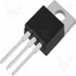
ICGOO电子元器件商城为您提供KSC5502DTTU由Fairchild Semiconductor设计生产,在icgoo商城现货销售,并且可以通过原厂、代理商等渠道进行代购。 KSC5502DTTU价格参考。Fairchild SemiconductorKSC5502DTTU封装/规格:晶体管 - 双极 (BJT) - 单, 双极 (BJT) 晶体管 NPN 600V 2A 11MHz 50W 通孔 TO-220-3。您可以下载KSC5502DTTU参考资料、Datasheet数据手册功能说明书,资料中有KSC5502DTTU 详细功能的应用电路图电压和使用方法及教程。
| 参数 | 数值 |
| 产品目录 | |
| 描述 | TRANS NPN 60V 2A TO-220 |
| 产品分类 | 晶体管(BJT) - 单路 |
| 品牌 | Fairchild Semiconductor |
| 数据手册 | |
| 产品图片 |
|
| 产品型号 | KSC5502DTTU |
| PCN设计/规格 | |
| rohs | 无铅 / 符合限制有害物质指令(RoHS)规范要求 |
| 产品系列 | - |
| 不同 Ib、Ic时的 Vce饱和值(最大值) | 1.5V @ 200mA,1A |
| 不同 Ic、Vce 时的DC电流增益(hFE)(最小值) | 4 @ 1A,1V |
| 供应商器件封装 | TO-220 |
| 功率-最大值 | 50W |
| 包装 | 管件 |
| 安装类型 | 通孔 |
| 封装/外壳 | TO-220-3 |
| 晶体管类型 | NPN |
| 标准包装 | 50 |
| 电压-集射极击穿(最大值) | 600V |
| 电流-集电极(Ic)(最大值) | 2A |
| 电流-集电极截止(最大值) | 100µA |
| 频率-跃迁 | 11MHz |


- 商务部:美国ITC正式对集成电路等产品启动337调查
- 曝三星4nm工艺存在良率问题 高通将骁龙8 Gen1或转产台积电
- 太阳诱电将投资9.5亿元在常州建新厂生产MLCC 预计2023年完工
- 英特尔发布欧洲新工厂建设计划 深化IDM 2.0 战略
- 台积电先进制程称霸业界 有大客户加持明年业绩稳了
- 达到5530亿美元!SIA预计今年全球半导体销售额将创下新高
- 英特尔拟将自动驾驶子公司Mobileye上市 估值或超500亿美元
- 三星加码芯片和SET,合并消费电子和移动部门,撤换高东真等 CEO
- 三星电子宣布重大人事变动 还合并消费电子和移动部门
- 海关总署:前11个月进口集成电路产品价值2.52万亿元 增长14.8%


PDF Datasheet 数据手册内容提取
Is Now Part of To learn more about ON Semiconductor, please visit our website at www.onsemi.com Please note: As part of the Fairchild Semiconductor integration, some of the Fairchild orderable part numbers will need to change in order to meet ON Semiconductor’s system requirements. Since the ON Semiconductor product management systems do not have the ability to manage part nomenclature that utilizes an underscore (_), the underscore (_) in the Fairchild part numbers will be changed to a dash (-). This document may contain device numbers with an underscore (_). Please check the ON Semiconductor website to verify the updated device numbers. The most current and up-to-date ordering information can be found at www.onsemi.com. Please email any questions regarding the system integration to Fairchild_questions@onsemi.com. ON Semiconductor and the ON Semiconductor logo are trademarks of Semiconductor Components Industries, LLC dba ON Semiconductor or its subsidiaries in the United States and/or other countries. ON Semiconductor owns the rights to a number of patents, trademarks, copyrights, trade secrets, and other intellectual property. A listing of ON Semiconductor’s product/patent coverage may be accessed at www.onsemi.com/site/pdf/Patent-Marking.pdf. ON Semiconductor reserves the right to make changes without further notice to any products herein. ON Semiconductor makes no warranty, representation or guarantee regarding the suitability of its products for any particular purpose, nor does ON Semiconductor assume any liability arising out of the application or use of any product or circuit, and specifically disclaims any and all liability, including without limitation special, consequential or incidental damages. Buyer is responsible for its products and applications using ON Semiconductor products, including compliance with all laws, regulations and safety requirements or standards, regardless of any support or applications information provided by ON Semiconductor. “Typical” parameters which may be provided in ON Semiconductor data sheets and/or specifications can and do vary in different applications and actual performance may vary over time. All operating parameters, including “Typicals” must be validated for each customer application by customer’s technical experts. ON Semiconductor does not convey any license under its patent rights nor the rights of others. ON Semiconductor products are not designed, intended, or authorized for use as a critical component in life support systems or any FDA Class 3 medical devices or medical devices with a same or similar classification in a foreign jurisdiction or any devices intended for implantation in the human body. Should Buyer purchase or use ON Semiconductor products for any such unintended or unauthorized application, Buyer shall indemnify and hold ON Semiconductor and its officers, employees, subsidiaries, affiliates, and distributors harmless against all claims, costs, damages, and expenses, and reasonable attorney fees arising out of, directly or indirectly, any claim of personal injury or death associated with such unintended or unauthorized use, even if such claim alleges that ON Semiconductor was negligent regarding the design or manufacture of the part. ON Semiconductor is an Equal Opportunity/Affirmative Action Employer. This literature is subject to all applicable copyright laws and is not for resale in any manner.
K S C 5 July 2014 5 0 2 D / K S KSC5502D / KSC5502DT C 5 5 NPN Triple Diffused Planar Silicon Transistor 0 2 D T — 4 Features D-PAK Equivalent Circuit N P • High Voltage Power Switch Switching Application C N • Wide Safe Operating Area 1 T 4 • Built-in Free-Wheeling Diode TO-220 r i B p • Suitable for Electronic Ballast Application l e • Small Variance in Storage Time D • Two Package Choices : D-PAK or TO-220 E 1 if f u 1.Base 2,4.Collector 3.Emitter s e d P Ordering Information l a n a Part Number Top Mark Package Packing Method r S KSC5502DTM C5502D TO-252 3L (DPAK) Tape and Reel i l i c KSC5502DTTU C5502D TO-220 3L Rail o n T r a Absolute Maximum Ratings n s i Stresses exceeding the absolute maximum ratings may damage the device. The device may not function or be opera- s t ble above the recommended operating conditions and stressing the parts to these levels is not recommended. In addi- o r tion, extended exposure to stresses above the recommended operating conditions may affect device reliability. The absolute maximum ratings are stress ratings only. Values are at T = 25°C unless otherwise noted. C Symbol Parameter Value Unit V Collector-Base Voltage 1200 V CBO V Collector-Emitter Voltage 600 V CEO V Emitter-Base Voltage 12 V EBO I Collector Current (DC) 2 A C I Collector Current (Pulse)(1) 4 A CP I Base Current (DC) 1 A B I Base Current (Pulse)(1) 2 A BP T Junction Temperature 150 °C J T Storage Temperature Range -65 to 150 °C STG EAS Avalanche Energy (T = 25°C) 2.5 mJ J Note: 1. Pulse test: Pulse width = 5 ms, duty cycle ≤ 10%. © 2000 Fairchild Semiconductor Corporation www.fairchildsemi.com KSC5502D / KSC5502DT Rev. 1.1.0
K S Thermal Characteristics C 5 Values are at T = 25°C unless otherwise noted. 5 C 0 2 KSC5502D KSC5502DT D Symbol Parameter Unit (D-PAK) (TO-220) / K P Collector Dissipation (T = 25°C) 87.83 118.16 W S C C C RθJC Thermal Resistance, Junction to Case 1.42 1.06 °C/W 5 5 RθJA Thermal Resistance, Junction to Ambient 111.0 62.5 °C/W 0 2 T Maximum Lead Temperature for Soldering Purpose: 270 °C D L 1/8 inch from Case for 5 seconds T — N Electrical Characteristics P N Values are at T = 25°C unless otherwise noted. C T r Symbol Parameter Conditions Min. Typ. Max. Unit i p l BV Collector-Base Breakdown Voltage I = 1 mA, I = 0 1200 1350 V e CBO C E D Collector-Emitter Breakdown BVCEO Voltage IC = 5 mA, IB = 0 600 750 V iff u BV Emitter-Base Breakdown Voltage I = 500 μA, I = 0 12.0 13.7 V s EBO E C e T = 25°C 100 d ICES Collector Cut-off Current VCES = 1200 V, VBE = 0 TCC = 125°C 500 μA Pla T = 25°C 100 n I Collector Cut-off Current V = 600 V, I = 0 C μA a CEO CE B TC = 125°C 500 r S I Emitter Cut-off Current V = 12 V, I = 0 T = 25°C 10 μA i EBO EB C C l i TC = 25°C 15 28 40 co V = 1 V, I = 0.2 A CE C T = 125°C 8 18 n C T T = 25°C 4.0 6.4 r h DC Current Gain V = 1 V, I = 1 A C a FE CE C T = 125°C 3.0 4.7 n C s VCE = 2.5 V, TC = 25°C 12 20 30 ist IC = 0.5 A TC = 125°C 6 12 or T = 25°C 0.31 0.80 C I = 0.2 A, I = 0.02 A C B T = 125°C 0.54 1.10 C Collector-Emitter Saturation TC = 25°C 0.15 0.60 V (sat) I = 0.4 A, I = 0.08 A V CE Voltage C B T = 125°C 0.23 1.00 C T = 25°C 0.40 1.50 C I = 1 A, I = 0.2 A C B T = 125°C 1.30 3.00 C T = 25°C 0.77 1.00 C I = 0.4 A, I = 0.08 A C B T = 125°C 0.60 0.90 C V (sat) Base-Emitter Saturation Voltage V BE T = 25°C 0.83 1.20 C I = 1 A, I = 0.2 A C B T = 125°C 0.70 1.00 C C Input Capacitance V = 8 V, I = 0, f = 1 MHz 385 500 pF ib EB C C Output Capacitance V = 10 V, I = 0, f = 1 MHz 60 100 pF ob CB E f Current Gain Bandwidth Product I = 0.5 A,V = 10 V 11 MHz T C CE T = 25°C 0.75 1.20 C I = 0.2 A F T = 125°C 0.59 C V Diode Forward Voltage T = 25°C 0.80 1.30 V F C I = 0.4 A F T = 125°C 0.64 C I = 1 A T = 25°C 0.90 1.50 F C © 2000 Fairchild Semiconductor Corporation www.fairchildsemi.com KSC5502D / KSC5502DT Rev. 1.1.0 2
K S Electrical Characteristics C 5 Values are at T = 25°C unless otherwise noted. 5 C 0 2 Symbol Parameter Conditions Min Typ. Max. Unit D IF = 0.2 A 650 / K Diode Froward Recovery t I = 0.4 A 740 ns S fr Time (di/dt=10 A/μs) F C IF = 1 A 785 5 5 I = 0.4 A, I = 80 mA, at 1 μs 7.2 0 C B1 2 VCC = 300 V at 3 μs 1.8 D VCE(DSAT) Dynamic Saturation Voltage IC = 1 A, IB1 = 200 mA, at 1 μs 18.0 V T — VCC = 300 V at 3 μs 6.0 N Resistive Load Switching (D.C < 10%, Pulse Width = 20 s) P T = 25°C 175 350 N tON Turn-On Time IC = 0.4 A, IB1 = 80 mA, TC = 125°C 185 ns Tr tOFF Turn-Off Time IRBL2 == 705.20 AΩ, VCC = 300 V, TTCCC == 2152°5C°C 22..16 3.0 μs iple D tON Turn-On Time IICB2 = = 1 1 A6,0 I Bm1A =, 160 mA, TTCC == 2152°5C°C 234100 450 ns iffuse tOFF Turn-Off Time VRCL C= =3 0300 0Ω V, TTC == 2152°5C°C 34..75 5.0 μs d P C l a Inductive Load Switching (V = 15 V) n CC a T = 25°C 1.2 2.0 r tSTG Storage Time TCC = 125°C 1.5 μs Sil IC = 0.4 A, IB1 = 80 mA, T = 25°C 90 200 ic t Fall Time I = 0.2 A, V = 300 V, C ns o F B2 Z T = 125°C 65 n LC = 200 H C T t Cross-Over Time TC = 25°C 185 350 ns ra C T = 125°C 145 n C s tSTG Storage Time TTC == 2152°5C°C 33..7305 4.50 μs isto IC = 0.8 A, IB1 = 160 mA, C r t Fall Time IB2 = 160 mA, TC = 25°C 90 250 ns F VCC = 300 V, TC = 125°C 160 LC = 200 H T = 25°C 300 600 C t Cross-over Time ns C T = 125°C 570 C © 2000 Fairchild Semiconductor Corporation www.fairchildsemi.com KSC5502D / KSC5502DT Rev. 1.1.0 3
K S Typical Performance Characteristics C 5 5 0 2 D 3 / K 1A RRENT 90800m07m0A06Am050A0m0AmA N 100 TJ=125oC VCE=1V SC55 OR CU 2 40300m0mAA NT GAI TJ=25oC 02D I[A], COLLECTC1 IB2=0100m0mAA h, DC CURREFE 10 T — NP N T 00 1 2 3 4 5 6 7 11m 10m 100m 1 rip V [V], COLLECTOR EMITTER VOLTAGE I [A], COLLECTOR CURRENT) l CE C e Figure 1. Static Characteristic Figure 2. DC Current Gain D i f f u s e d P l IC=5IB IC=10IB a n 10 10 a V(V), VOLTAGECE(sat) 1 TJ=125oC V(V), VOLTAGECE(sat) 1 TJ=125oC r Silicon T TJ=25oC TJ=25oC ran 0.1 0.1 s i s 1m 10m 100m 1 1m 10m 100m 1 to I (A), COLLECTOR CURRENT I (A), COLLECTOR CURRENT r C C Figure 3. Collector-Emitter Saturation Voltage Figure 4. Collector-Emitter Saturation Voltage 2 10 TJ=25oC IC=10IB 2.0A 1.5A E E G G TA 1.0A TA L L V], VO 1 0.4A V], VO 1 TJ=25oC V[CE IC=0.2A V[BE TJ=125oC 0 0.1 1m 10m 100m 1 1m 10m 100m 1 I[A], BASE CURRENT I [A], COLLECTOR CURRENT B C Figure 5. Typical Collector Saturation Voltage Figure 6. Base-Emitter Saturation Voltage © 2000 Fairchild Semiconductor Corporation www.fairchildsemi.com KSC5502D / KSC5502DT Rev. 1.1.0 4
K S Typical Performance Characteristics (Continued) C 5 5 0 2 D / 10 10 K S IC=5IB C 5 5 E E 0 V], VOLTAG 1 TJ=25oC V], VOLTAG 1 TJ=25oC 2DT — V[BE TJ=125oC V[FD TJ=125oC N P N T r 0.1 0.1 i 1m 10m 100m 1 1m 10m 100m 1 p IC[A], COLLECTOR CURRENT IFD[A], FORWARD CURRENT le Figure 7. Base-Emitter Saturation Voltage Figure 8. Diode Forward Voltage D i f f u s e d 1000 2000 P Cib F=1MHz IVPCWC=C5==IB32100=0μ2VsIB2 lan a E[pF] 11008900000000 r S C E 700 CAPACITAN 100 Cob t[ns],TIMON 345600000000 TJ=125oC ilicon TJ=25oC Tr 200 a n s i s 101 10 100 1100000.3 0.5 1 1.5 2 2.5 3 to REVERSE VOLTAGE[V] IC[A], COLLECTOR CURRENT r Figure 9. Collector Output Capacitance Figure 10. Resistive Switching Time, t on 5 4.5 2000 3.54 IVPC=CWC5==IB3210=002μVIsB2 IVPC=cW=53=IB0210=0V5μIsB2 11000000 3 890000 TJ=125oC E E 700 μt(s),TIMON2.25 TJ=125oC t(ns),TIMON 345600000000 TJ=25oC 1.5 TJ=25oC 200 1 110000 0.3 0.5 1 1.5 2 2.5 3 0.3 0.5 1 1.5 2 2.5 3 I[A], COLLECTOR CURRENT I [A], COLLECTOR CURRENT C C Figure 11. Resistive Switching Time, t Figure 12. Resistive Switching Time, t off on © 2000 Fairchild Semiconductor Corporation www.fairchildsemi.com KSC5502D / KSC5502DT Rev. 1.1.0 5
K S Typical Performance Characteristics (Continued) C 5 5 0 2 D 7 3 / K 6.5 5.556 IVPC=cW=53=IB0210=0V5μIsB2 2.5 IVVLCCCZ===C5=32I1B001500=VVμ2HIB2 SC55 μt(s),TIMEON 34..545 TJ=25oC TJ=125oC μt(s),TIMESTG 1.52 TJ=125oC 02DT — 3 TJ=25oC N P 2.5 N T 20.3 0.5 1 1.5 2 2.5 3 10.3 0.5 1 1.5 2 2.5 3 rip IC[A], COLLECTOR CURRENT IC[A], COLLECTOR CURRENT le Figure 13. Resistive Switching Time, t Figure 14. Inductive Switching Time, t D off STG i f f u s e d 110 600 1089000 IVVLCC=CZ==C5=23IB1001500=VμV2HIB2 344555050500000 IVVLCC=CZ==C5=23I1B001500=VμV2HIB2 Planar S t(ns),TIMEF 6700 TJ=25oC TJ=125oC t[ns],TIMEC 223050000 TJ=125oC ilicon TJ=25oC Tr 50 150 a n s i s 400.3 0.5 1 1.5 2 2.5 3 1000.3 0.5 1 1.5 2 2.5 3 to IC[A], COLLECTOR CURRENT IC[A], COLLECTOR CURRENT r Figure 15. Inductive Switching Time, t Figure 16. Inductive Switching Time, t F c 5 1000 900 4.45 IVVLCC=CZ==C5=23I1B001500=VμV5HIB2 TJ=125oC 456780000000000 IVVLCC=CZ==C5=23IB1001500=VμV5HIB2 ME 3.5 ME 300 TJ=125oC μt[s],TISTG 3 TJ=25oC t[ns],TIF 200 TJ=25oC 2.5 100 90 80 70 60 2 50 0.3 0.5 1 1.5 2 2.5 3 0.3 0.5 1 1.5 2 2.5 3 I [A], COLLECTOR CURRENT I [A], COLLECTOR CURRENT C C Figure 17. Inductive Switching Time, t Figure 18. Inductive Switching Time, t STG F © 2000 Fairchild Semiconductor Corporation www.fairchildsemi.com KSC5502D / KSC5502DT Rev. 1.1.0 6
K S Typical Performance Characteristics (Continued) C 5 5 0 2 D 2000 2.0 / K 11008900000000 IVVLCC=CZ==C5=23I1B001500=VμV5HIB2 TJ=125oC 11..68 IC=0.8A IVVLCC=CZ==C2=23I1B002500VμVH SC550 t[ns],TIMESTG 345670000000000 TJ=25oC μt, TIME[s]STG 111...024 TTJJ==12255oCoC 2DT — N 200 0.8 IC=0.4A PN 0.6 T 1100000.3 0.5 1 1.5 2 2.5 3 0.44 5 6 7 8 9 10 11 12 13 14 rip IC[A], COLLECTOR CURRENT hFE, FORCED GAIN le Figure 19. Inductive Switching Time, t Figure 20. Inductive Switching Time, t D c STG i f f u s e d 200 80 IC=0.8A IVVLCCCZ===C2=32I1B002500VVμH IVVLCCCZ===C2=32I1B002500VVμH Plana r 160 t, TIME[ns]F 60 TTJJ==12255oCoC t, TIME[ns]C 120 IC=0.8A TTJJ==12255oCoC Silicon T r IC=0.4A a 40 IC=0.4A n s i s 4 5 6 7 8 9 10 11 12 13 14 804 5 6 7 8 9 10 11 12 13 14 to hFE, FORCED GAIN hFE, FORCED GAIN r Figure 21. Inductive Switching Time, t Figure 22. Inductive Switching Time, t F c 10 140 TC=25oC 130 5ms 1ms 50μs 120 CTOR CURRENT 1 DC R DISSIPATION 110178900000 D-PAK TO-220 COLLE 0.1 POWE 5600 A], W], 40 I[C P[C 30 20 10 0.01 0 10 100 1000 0 25 50 75 100 125 150 175 200 VCE[A], COLLECTOR EMITTER VOLTAGE TC(oC), CASE TEMPERATURE Figure 23. Forward Bias Safe Operating Area Figure 24. Power Derating © 2000 Fairchild Semiconductor Corporation www.fairchildsemi.com KSC5502D / KSC5502DT Rev. 1.1.0 7
K S Typical Performance Characteristics (Continued) C 5 5 0 2 D 10 10 / C A K J J o o 1 S Z Z 0.5 pedance 1 0.5 pedance 0.1 0000..0.0.1225 C550 m 0.2 m0.01 2 hermal i 0.1 000...0000.1251 hermal i1E-3 0.01 DT — alized T0.01 Single alized T1E-4 NP m m or or1E-5 Single N N N T 1E-31E-5 1E-4 1E-3 0.01 0.1 1 1E-61E-6 1E-5 1E-4 1E-3 0.01 0.1 1 10 100 1000 rip t, Rectangular Pulse Duration t, Rectangular Pulse Duration l e Figure 25. ZoJC, Transient Thermal Impedance Figure 26. ZoJA, Transient Thermal Impedance D i (D-PAK) (D-PAK) f f u s e d 10 10 P JC JA la Zo Zo 1 0.5 n e e 0.2 a mal impedanc 0.11 0000.0...1525 mal impedanc0.00.11 0000...0.001125 r Silico er 0.02 er1E-3 n h 0.01 h T T T alized 0.01 Single alized 1E-4 ran orm orm1E-5 Single si N N s t o 1E-3 1E-6 1E-5 1E-4 1E-3 0.01 0.1 1 1E-6 1E-5 1E-4 1E-3 0.01 0.1 1 10 100 1000 r t, Rectangular Pulse Duration t, Rectangular Pulse Duration Figure 27. ZoJC, Transient Thermal Impedance Figure 28. ZoJA, Transient Thermal Impedance (TO-220) (TO-220) © 2000 Fairchild Semiconductor Corporation www.fairchildsemi.com KSC5502D / KSC5502DT Rev. 1.1.0 8
K S Physical Dimensions C 5 5 0 2 D / K S C 5 5 0 2 D T — N P N T r i p l e D i f f u s e d P l a n a r S i l i c o n T r a n s i s t o r Figure 29. TO-252 (D-PAK), MOLDED, 3-LEAD, OPTION AA & AB Package drawings are provided as a service to customers considering Fairchild components. Drawings may change in any manner without notice. Please note the revision and/or date on the drawing and contact a Fairchild Semiconductor representative to verify or obtain the most recent revision. Package specifications do not expand the terms of Fairchild’s worldwide terms and conditions, specifically the warranty therein, which covers Fairchild products. Always visit Fairchild Semiconductor’s online packaging area for the most recent package drawings: http://www.fairchildsemi.com/dwg/TO/TO252A03.pdf. For current tape and reel specifications, visit Fairchild Semiconductor’s online packaging area: http://www.fairchildsemi.com/packing_dwg/PKG-TO252A03.pdf. © 2000 Fairchild Semiconductor Corporation www.fairchildsemi.com KSC5502D / KSC5502DT Rev. 1.1.0 9
K S Physical Dimensions C 5 5 0 2 D / K S C 5 5 0 2 D T — N P N T r i p l e D i f f u s e d P l a n a r S i l i c o n T r a n s i s t o r Figure 30. TO-220, MOLDED, 3LEAD, JEDEC VARIATION AB Package drawings are provided as a service to customers considering Fairchild components. Drawings may change in any manner without notice. Please note the revision and/or date on the drawing and contact a Fairchild Semiconductor representative to verify or obtain the most recent revision. Package specifications do not expand the terms of Fairchild’s worldwide terms and conditions, specifically the warranty therein, which covers Fairchild products. Always visit Fairchild Semiconductor’s online packaging area for the most recent package drawings: http://www.fairchildsemi.com/dwg/TO/TO220B03.pdf. For current tape and reel specifications, visit Fairchild Semiconductor’s online packaging area: http://www.fairchildsemi.com/packing_dwg/PKG-TO220B03.pdf. © 2000 Fairchild Semiconductor Corporation www.fairchildsemi.com KSC5502D / KSC5502DT Rev. 1.1.0 10
TRADEMARKS The following includes registered and unregistered trademarks and service marks, owned by Fairchild Semiconductor and/or its global subsidiaries, and is not intended to be an exhaustive list of all such trademarks. AccuPower(cid:2) F-PFS(cid:2) AX-CAP®* FRFET® ® ®* BitSiC(cid:2) Global Power ResourceSM PowerTrench® TinyBoost® Build it Now(cid:2) GreenBridge(cid:2) PowerXS™ TinyBuck® CorePLUS(cid:2) Green FPS(cid:2) Programmable Active Droop(cid:2) TinyCalc(cid:2) CorePOWER(cid:2) Green FPS(cid:2) e-Series(cid:2) QFET® TinyLogic® CROSSVOLT(cid:2) Gmax(cid:2) QS(cid:2) TINYOPTO(cid:2) CTL(cid:2) GTO(cid:2) Quiet Series(cid:2) TinyPower(cid:2) Current Transfer Logic(cid:2) IntelliMAX(cid:2) RapidConfigure(cid:2) TinyPWM(cid:2) DEUXPEED® ISOPLANAR(cid:2) (cid:2) TinyWire(cid:2) Dual Cool™ Making Small Speakers Sound Louder TranSiC(cid:2) EcoSPARK® and Better™ Saving our world, 1mW/W/kWat a time™ TriFault Detect(cid:2) EfficientMax(cid:2) MegaBuck(cid:2) SignalWise(cid:2) TRUECURRENT®* ESBC(cid:2) MICROCOUPLER(cid:2) SmartMax(cid:2) (cid:3)SerDes(cid:2) ® MicroFET(cid:2) SMART START(cid:2) FFFFFFFFaAPAAEaasiiCSCSTrrtccB(cid:2)TvTThhC®e® iiQll noddcur ®eShi e(cid:2)(cid:2)et m Siecroiensd(cid:2)uc tor® MMMMmOOOPpPWioiilcclttTTerroiSooorOOHDnPaPPLiMvrTaaOieLkvk(cid:2)arAe2(cid:2)G®x (cid:2)N(cid:2) (cid:2)I CA ®R ® SSSSSSSSSuTouuPuuypnpplppEMuecereeAte®rFirrrSoL FMSSEnOTEOOTOsHTT(cid:2) TTSf(cid:2)(cid:2)®o(cid:2)(cid:2) ® -r 3-- Y68 our Success(cid:2) UUUVVVXCioSHlnstrli™XuCtFaaa(cid:2)E ®g Fl MTe R(cid:2)PaFlx uE(cid:2) sT(cid:2)(cid:2) Sync-Lock™ (cid:3037)(cid:10106)™ * Trademarks of System General Corporation, used under license by Fairchild Semiconductor. DISCLAIMER FAIRCHILD SEMICONDUCTOR RESERVES THE RIGHT TO MAKE CHANGES WITHOUT FURTHER NOTICE TO ANY PRODUCTS HEREIN TO IMPROVE RELIABILITY, FUNCTION, OR DESIGN. FAIRCHILD DOES NOT ASSUME ANY LIABILITY ARISING OUT OF THE APPLICATION OR USE OF ANY PRODUCT OR CIRCUIT DESCRIBED HEREIN; NEITHER DOES IT CONVEY ANY LICENSE UNDER ITS PATENT RIGHTS, NOR THE RIGHTS OF OTHERS. THESE SPECIFICATIONS DO NOT EXPAND THE TERMS OF FAIRCHILD’S WORLDWIDE TERMS AND CONDITIONS, SPECIFICALLY THE WARRANTY THEREIN, WHICH COVERS THESE PRODUCTS. LIFE SUPPORT POLICY FAIRCHILD’S PRODUCTS ARE NOT AUTHORIZED FOR USE AS CRITICAL COMPONENTS IN LIFE SUPPORT DEVICES OR SYSTEMS WITHOUT THE EXPRESS WRITTEN APPROVAL OF FAIRCHILD SEMICONDUCTOR CORPORATION. As used herein: 1. Life support devices or systems are devices or systems which, (a) are 2. A critical component in any component of a life support, device, or intended for surgical implant into the body or (b) support or sustain system whose failure to perform can be reasonably expected to life, and (c) whose failure to perform when properly used in cause the failure of the life support device or system, or to affect its accordance with instructions for use provided in the labeling, can be safety or effectiveness. reasonably expected to result in a significant injury of the user. ANTI-COUNTERFEITING POLICY Fairchild Semiconductor Corporation's Anti-Counterfeiting Policy. Fairchild's Anti-Counterfeiting Policy is also stated on our external website, www.fairchildsemi.com, under Sales Support. Counterfeiting of semiconductor parts is a growing problem in the industry. All manufacturers of semiconductor products are experiencing counterfeiting of their parts. Customers who inadvertently purchase counterfeit parts experience many problems such as loss of brand reputation, substandard performance, failed applications, and increased cost of production and manufacturing delays. Fairchild is taking strong measures to protect ourselves and our customers from the proliferation of counterfeit parts. Fairchild strongly encourages customers to purchase Fairchild parts either directly from Fairchild or from Authorized Fairchild Distributors who are listed by country on our web page cited above. Products customers buy either from Fairchild directly or from Authorized Fairchild Distributors are genuine parts, have full traceability, meet Fairchild's quality standards for handling and storage and provide access to Fairchild's full range of up-to-date technical and product information. Fairchild and our Authorized Distributors will stand behind all warranties and will appropriately address any warranty issues that may arise. Fairchild will not provide any warranty coverage or other assistance for parts bought from Unauthorized Sources. Fairchild is committed to combat this global problem and encourage our customers to do their part in stopping this practice by buying direct or from authorized distributors. PRODUCT STATUS DEFINITIONS Definition of Terms Datasheet Identification Product Status Definition Datasheet contains the design specifications for product development. Specifications may change Advance Information Formative / In Design in any manner without notice. Datasheet contains preliminary data; supplementary data will be published at a later date. Fairchild Preliminary First Production Semiconductor reserves the right to make changes at any time without notice to improve design. Datasheet contains final specifications. Fairchild Semiconductor reserves the right to make No Identification Needed Full Production changes at any time without notice to improve the design. Datasheet contains specifications on a product that is discontinued by Fairchild Semiconductor. Obsolete Not In Production The datasheet is for reference information only. Rev. I68 © Fairchild Semiconductor Corporation www.fairchildsemi.com
ON Semiconductor and are trademarks of Semiconductor Components Industries, LLC dba ON Semiconductor or its subsidiaries in the United States and/or other countries. ON Semiconductor owns the rights to a number of patents, trademarks, copyrights, trade secrets, and other intellectual property. A listing of ON Semiconductor’s product/patent coverage may be accessed at www.onsemi.com/site/pdf/Patent−Marking.pdf. ON Semiconductor reserves the right to make changes without further notice to any products herein. ON Semiconductor makes no warranty, representation or guarantee regarding the suitability of its products for any particular purpose, nor does ON Semiconductor assume any liability arising out of the application or use of any product or circuit, and specifically disclaims any and all liability, including without limitation special, consequential or incidental damages. Buyer is responsible for its products and applications using ON Semiconductor products, including compliance with all laws, regulations and safety requirements or standards, regardless of any support or applications information provided by ON Semiconductor. “Typical” parameters which may be provided in ON Semiconductor data sheets and/or specifications can and do vary in different applications and actual performance may vary over time. All operating parameters, including “Typicals” must be validated for each customer application by customer’s technical experts. ON Semiconductor does not convey any license under its patent rights nor the rights of others. ON Semiconductor products are not designed, intended, or authorized for use as a critical component in life support systems or any FDA Class 3 medical devices or medical devices with a same or similar classification in a foreign jurisdiction or any devices intended for implantation in the human body. Should Buyer purchase or use ON Semiconductor products for any such unintended or unauthorized application, Buyer shall indemnify and hold ON Semiconductor and its officers, employees, subsidiaries, affiliates, and distributors harmless against all claims, costs, damages, and expenses, and reasonable attorney fees arising out of, directly or indirectly, any claim of personal injury or death associated with such unintended or unauthorized use, even if such claim alleges that ON Semiconductor was negligent regarding the design or manufacture of the part. ON Semiconductor is an Equal Opportunity/Affirmative Action Employer. This literature is subject to all applicable copyright laws and is not for resale in any manner. PUBLICATION ORDERING INFORMATION LITERATURE FULFILLMENT: N. American Technical Support: 800−282−9855 Toll Free ON Semiconductor Website: www.onsemi.com Literature Distribution Center for ON Semiconductor USA/Canada 19521 E. 32nd Pkwy, Aurora, Colorado 80011 USA Europe, Middle East and Africa Technical Support: Order Literature: http://www.onsemi.com/orderlit Phone: 303−675−2175 or 800−344−3860 Toll Free USA/Canada Phone: 421 33 790 2910 Fax: 303−675−2176 or 800−344−3867 Toll Free USA/Canada Japan Customer Focus Center For additional information, please contact your local Email: orderlit@onsemi.com Phone: 81−3−5817−1050 Sales Representative © Semiconductor Components Industries, LLC www.onsemi.com www.onsemi.com 1
Mouser Electronics Authorized Distributor Click to View Pricing, Inventory, Delivery & Lifecycle Information: O N Semiconductor: KSC5502DTTU