ICGOO在线商城 > 分立半导体产品 > 晶体管 - FET,MOSFET - 射频 > J310G
 Datasheet下载
- 型号: J310G
- 制造商: ON Semiconductor
- 库位|库存: xxxx|xxxx
- 要求:
| 数量阶梯 | 香港交货 | 国内含税 |
| +xxxx | $xxxx | ¥xxxx |
查看当月历史价格
查看今年历史价格
J310G产品简介:
ICGOO电子元器件商城为您提供J310G由ON Semiconductor设计生产,在icgoo商城现货销售,并且可以通过原厂、代理商等渠道进行代购。 J310G价格参考。ON SemiconductorJ310G封装/规格:晶体管 - FET,MOSFET - 射频, 射频 Mosfet N 通道 JFET 10V 10mA 100MHz 16dB TO-92-3。您可以下载J310G参考资料、Datasheet数据手册功能说明书,资料中有J310G 详细功能的应用电路图电压和使用方法及教程。
| 参数 | 数值 |
| 产品目录 | |
| 描述 | JFET VHF/UHF N-CH 25V TO92JFET 25V 10mA |
| 产品分类 | RF FET分离式半导体 |
| 品牌 | ON Semiconductor |
| 产品手册 | |
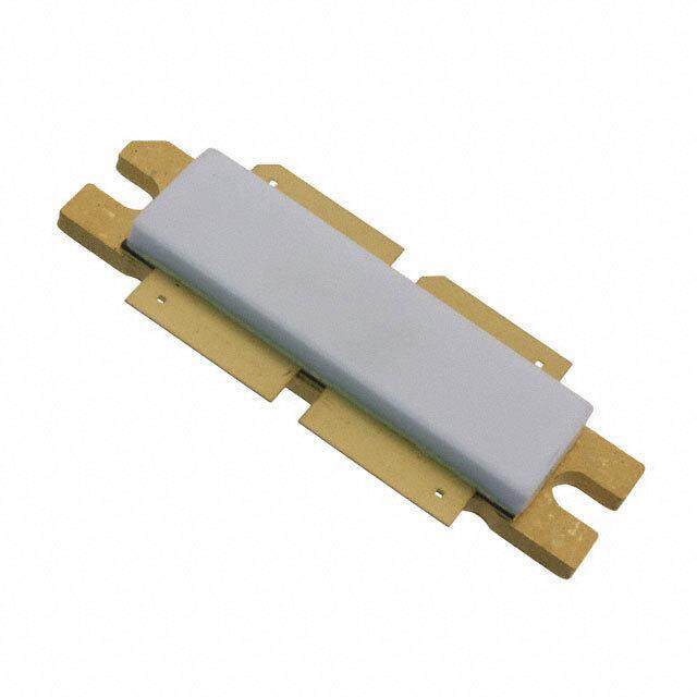
| 产品图片 |
|
| rohs | 符合RoHS无铅 / 符合限制有害物质指令(RoHS)规范要求 |
| 产品系列 | 晶体管,JFET,ON Semiconductor J310G- |
| 数据手册 | |
| 产品型号 | J310G |
| Vds-Drain-SourceBreakdownVoltage | 25 V |
| Vds-漏源极击穿电压 | 25 V |
| Vgs-Gate-SourceBreakdownVoltage | 25 V |
| Vgs-栅源极击穿电压 | 25 V |
| Vgs=0时的漏-源电流 | 24 mA to 60 mA |
| 产品目录页面 | |
| 产品种类 | JFET |
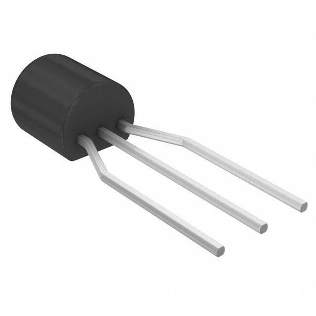
| 供应商器件封装 | TO-92-3 |
| 其它名称 | J310GOS |
| 功率-输出 | - |
| 包装 | 散装 |
| 商标 | ON Semiconductor |
| 噪声系数 | - |
| 增益 | 16dB |
| 安装风格 | Through Hole |
| 封装 | Bulk |
| 封装/外壳 | TO-226-3、TO-92-3 标准主体 |
| 封装/箱体 | TO-92-3 |
| 工厂包装数量 | 1000 |
| 晶体管极性 | N-Channel |
| 晶体管类型 | N 通道 JFET |
| 标准包装 | 1,000 |
| 漏源电压VDS | 25 V |
| 电压-测试 | 10V |
| 电压-额定 | 25V |
| 电流-测试 | 10mA |
| 系列 | J310 |
| 配置 | Single |
| 闸/源击穿电压 | 25 V |
| 频率 | 100MHz |
| 额定电流 | 60mA |

,TO-226_straightlead.jpg)


- 商务部:美国ITC正式对集成电路等产品启动337调查
- 曝三星4nm工艺存在良率问题 高通将骁龙8 Gen1或转产台积电
- 太阳诱电将投资9.5亿元在常州建新厂生产MLCC 预计2023年完工
- 英特尔发布欧洲新工厂建设计划 深化IDM 2.0 战略
- 台积电先进制程称霸业界 有大客户加持明年业绩稳了
- 达到5530亿美元!SIA预计今年全球半导体销售额将创下新高
- 英特尔拟将自动驾驶子公司Mobileye上市 估值或超500亿美元
- 三星加码芯片和SET,合并消费电子和移动部门,撤换高东真等 CEO
- 三星电子宣布重大人事变动 还合并消费电子和移动部门
- 海关总署:前11个月进口集成电路产品价值2.52万亿元 增长14.8%


PDF Datasheet 数据手册内容提取
J309, J310 Preferred Device JFET VHF/UHF Amplifiers N−Channel — Depletion Features • Pb−Free Packages are Available* http://onsemi.com 1 DRAIN MAXIMUM RATINGS Rating Symbol Value Unit 3 Drain−Source Voltage VDS 25 Vdc GATE Gate−Source Voltage VGS 25 Vdc Forward Gate Current IGF 10 mAdc 2 SOURCE Total Device Dissipation @ TA = 25°C PD 350 mW Derate above = 25°C 2.8 mW/°C Junction Temperature Range TJ −65 to +125 °C Storage Temperature Range Tstg −65 to +150 °C Maximum ratings are those values beyond which device damage can occur. Maximum ratings applied to the device are individual stress limit values (not normal operating conditions) and are not valid simultaneously. If these limits are TO−92 exceeded, device functional operation is not implied, damage may occur and CASE 29−11 reliability may be affected. 12 STYLE 5 3 MARKING DIAGRAM J3xx AYWW(cid:2) (cid:2) J3xx =Device Code xx = 09 or 10 A =Assembly Location Y =Year WW =Work Week (cid:2) =Pb−Free Package (Note: Microdot may be in either location) ORDERING INFORMATION See detailed ordering and shipping information in the package dimensions section on page 3 of this data sheet. Preferred devices are recommended choices for future use *For additional information on our Pb−Free strategy and soldering details, please and best overall value. download the ON Semiconductor Soldering and Mounting Techniques Reference Manual, SOLDERRM/D. © Semiconductor Components Industries, LLC, 2006 1 Publication Order Number: March, 2006 − Rev. 1 J309/D
J309, J310 ELECTRICAL CHARACTERISTICS (TA = 25°C unless otherwise noted) Characteristic Symbol Min Typ Max Unit OFF CHARACTERISTICS Gate−Source Breakdown Voltage V(BR)GSS −25 − − Vdc (IG = −1.0 (cid:2)Adc, VDS = 0) Gate Reverse Current IGSS (VGS = −15 Vdc, VDS = 0, TA = 25°C) − − −1.0 nAdc (VGS = −15 Vdc, VDS = 0, TA = +125°C) − − −1.0 (cid:2)Adc Gate Source Cutoff Voltage VGS(off) Vdc (VDS = 10 Vdc, ID = 1.0 nAdc) J309 −1.0 − −4.0 J310 −2.0 − −6.5 ON CHARACTERISTICS Zero−Gate−Voltage Drain Current(1) IDSS mAdc (VDS = 10 Vdc, VGS = 0) J309 12 − 30 J310 24 − 60 Gate−Source Forward Voltage VGS(f) − − 1.0 Vdc (VDS = 0, IG = 1.0 mAdc) SMALL−SIGNAL CHARACTERISTICS Common−Source Input Conductance Re(yis) mmhos (VDS = 10 Vdc, ID = 10 mAdc, f = 100 MHz) J309 − 0.7 − J310 − 0.5 − Common−Source Output Conductance Re(yos) − 0.25 − mmhos (VDS = 10 Vdc, ID = 10 mAdc, f = 100 MHz) Common−Gate Power Gain Gpg − 16 − dB (VDS = 10 Vdc, ID = 10 mAdc, f = 100 MHz) Common−Source Forward Transconductance Re(yfs) − 12 − mmhos (VDS = 10 Vdc, ID = 10 mAdc, f = 100 MHz) Common−Gate Input Conductance Re(yig) − 12 − mmhos (VDS = 10 Vdc, ID = 10 mAdc, f = 100 MHz) Common−Source Forward Transconductance gfs (cid:2)mhos (VDS = 10 Vdc, ID = 10 mAdc, f = 1.0 kHz) J309 10000 − 20000 J310 8000 − 18000 Common−Source Output Conductance gos − − 250 (cid:2)mhos (VDS = 10 Vdc, ID = 10 mAdc, f = 1.0 kHz) Common−Gate Forward Transconductance gfg (cid:2)mhos (VDS = 10 Vdc, ID = 10 mAdc, f = 1.0 kHz) J309 − 13000 − J310 − 12000 − Common−Gate Output Conductance gog (cid:2)mhos (VDS = 10 Vdc, ID = 10 mAdc, f = 1.0 kHz) J309 − 100 − J310 − 150 − Gate−Drain Capacitance Cgd − 1.8 2.5 pF (VDS = 0, VGS = −10 Vdc, f = 1.0 MHz) Gate−Source Capacitance Cgs − 4.3 5.0 pF (VDS = 0, VGS = −10 Vdc, f = 1.0 MHz) FUNCTIONAL CHARACTERISTICS Equivalent Short−Circuit Input Noise Voltage en − 10 − nV(cid:2)(cid:3)Hz (VDS = 10 Vdc, ID = 10 mAdc, f = 100 Hz) 1. Pulse Test: Pulse Width (cid:4) 300 (cid:2)s, Duty Cycle (cid:4) 3.0%. http://onsemi.com 2
J309, J310 ORDERING INFORMATION Device Package Shipping† J309 TO−92 J309G TO−92 1000 Units / Bulk (Pb−Free) J310 TO−92 J310G TO−92 1000 Units / Bulk (Pb−Free) J310RLRP TO−92 J310RLRPG TO−92 2000 Units / Tape & Ammo Box (Pb−Free) J310ZL1 TO−92 J310ZL1G TO−92 2000 Units / Tape & Ammo Box (Pb−Free) †For information on tape and reel specifications, including part orientation and tape sizes, please refer to our Tape and Reel Packaging Specifications Brochure, BRD8011/D. 70 70 os) 35 A) mh m m A) 60 VDS = 10 V TA = −(cid:2)55°C 60 RENT ( NCE ( 30 Vf =D S1 .=0 1M0H Vz TA = −(cid:2)55°C +(cid:2)25°C RRENT (m 5400 I+D(cid:2)2S5S°C +(cid:2)25°C 5400 RAIN CUR ONDUCTA 2250 , DRAIN CUID 321000 −(cid:2)55°+C(cid:2)25°C++115500°°CC 321000 , SATURATION DSS FORWARD TRANSC511.500 −(cid:2)5+51°5C0°C+150°+C(cid:2)25°C ID , s 0 Yf 0 −5.0 −4.0 −3.0 −2.0 −1.0 0 5.0 4.0 3.0 2.0 1.0 0 ID − VGS, GATE−SOURCE VOLTAGE (VOLTS) VGS, GATE−SOURCE VOLTAGE (VOLTS) IDSS − VGS, GATE−SOURCE CUTOFF VOLTAGE (VOLTS) Figure 1. Drain Current and Transfer Figure 2. Forward Transconductance Characteristics versus Gate−Source Voltage versus Gate−Source Voltage http://onsemi.com 3
J309, J310 os)100 k 1.0 k 10 120 h m μD TRANSCONDUCTANCE ( 11.00 kk VGS(ofYf) f=s −(cid:2)2.3 V = Yfs 11000μTPUT ADMITTANCE ( mhos) CAPACITANCE (pF)74..00 RDSCgs 974628ON RESISTANCE (OHMS) AR Yos VGS(off) = −(cid:2)5.7 V = OU , S ORW , Yos Cgd 24RD F 1.0 , s Yf 100 1.0 0 0 0.01 0.10.20.30.5 1.0 2.03.05.0 10 2030 50 100 10 9.0 8.0 7.0 6.0 5.0 4.0 3.0 2.0 1.0 0 ID, DRAIN CURRENT (mA) VGS, GATE SOURCE VOLTAGE (VOLTS) Figure 3. Common−Source Output Figure 4. On Resistance and Junction Admittance and Forward Transconductance Capacitance versus Gate−Source Voltage versus Drain Current |S21|, |S11| |S12|, |S22| 30 3.0 0.85 0.45 0.060 1.00 24 VDS = 10 V 2.4 0.79 0.39 S22 0.048 0.98 | (mmhos)22 18 ITDA == 1205 °mCA Y11 1.8mhos) 0.73 0.33 VIDD =S 1=0 1 m0 AV S21 0.036 0.96 Y|, |Y21 12 Y21 1.2Y(m12 0.67 0.27 TA = 25°C 0.024 0.94 |Y|, |11 6.0 Y22 0.6 0.61 0.21 S11 0.012 0.92 Y12 S12 0 0.55 0.15 0.90 100 200 300 500 700 1000 100 200 300 500 700 1000 f, FREQUENCY (MHz) f, FREQUENCY (MHz) Figure 5. Common−Gate Y Parameter Figure 6. Common−Gate S Parameter Magnitude versus Frequency Magnitude versus Frequency (cid:3)21, (cid:3)11 (cid:3)12, (cid:3)22 (cid:3)11, (cid:3)12 (cid:3)21, (cid:3)22 180° 50° −(cid:2)20° 87° −(cid:2)20° 120° 0 (cid:3) (cid:3)22 −(cid:2)20° 11 (cid:3) 170° 40° (cid:3) −(cid:2)40° 86° −(cid:2)40° 100° 21 (cid:3)22 −(cid:2)20° 21 −(cid:2)60° 160° 30° −(cid:2)80° 85° −(cid:2)60° 80° −(cid:2)40° −(cid:2)100° 150° 20° (cid:3)12 −(cid:2)120° 84° −(cid:2)80° 60° (cid:3)21 −(cid:2)60° (cid:3) −(cid:2)140° (cid:3) 11 12 140° 10° VDS = 10 V −(cid:2)160° 83° −(cid:2)100° 40° VDS = 10 V (cid:3) −(cid:2)80° ITDA == 1205 °mCA −(cid:2)180° ITDA == 1205 °mCA 11 130° 0° −(cid:2)200° 82° −(cid:2)120° 20° −(cid:2)100° 100 200 300 500 700 1000 100 200 300 500 700 1000 f, FREQUENCY (MHz) f, FREQUENCY (MHz) Figure 7. Common−Gate Y Parameter Figure 8. S Parameter Phase−Angle Phase−Angle versus Frequency versus Frequency http://onsemi.com 4
J309, J310 PACKAGE DIMENSIONS TO−92 (TO−226) CASE 29−11 ISSUE AL A NOTES: B 1. DIMENSIONING AND TOLERANCING PER ANSI Y14.5M, 1982. 2. CONTROLLING DIMENSION: INCH. R 3. CONTOUR OF PACKAGE BEYOND DIMENSION R IS UNCONTROLLED. 4. LEAD DIMENSION IS UNCONTROLLED IN P AND P BEYOND DIMENSION K MINIMUM. L SEATING INCHES MILLIMETERS PLANE K DIM MIN MAX MIN MAX A 0.175 0.205 4.45 5.20 B 0.170 0.210 4.32 5.33 C 0.125 0.165 3.18 4.19 X X D GD 00..001465 00..002515 0.14.0175 0.15.3339 G H 0.095 0.105 2.42 2.66 H J J 0.015 0.020 0.39 0.50 K 0.500 −−− 12.70 −−− V C L 0.250 −−− 6.35 −−− N 0.080 0.105 2.04 2.66 SECTION X−X P −−− 0.100 −−− 2.54 1 N R 0.115 −−− 2.93 −−− V 0.135 −−− 3.43 −−− N STYLE 5: PIN 1. DRAIN 2. SOURCE 3. GATE ON Semiconductor and are registered trademarks of Semiconductor Components Industries, LLC (SCILLC). SCILLC reserves the right to make changes without further notice to any products herein. SCILLC makes no warranty, representation or guarantee regarding the suitability of its products for any particular purpose, nor does SCILLC assume any liability arising out of the application or use of any product or circuit, and specifically disclaims any and all liability, including without limitation special, consequential or incidental damages. “Typical” parameters which may be provided in SCILLC data sheets and/or specifications can and do vary in different applications and actual performance may vary over time. All operating parameters, including “Typicals” must be validated for each customer application by customer’s technical experts. SCILLC does not convey any license under its patent rights nor the rights of others. SCILLC products are not designed, intended, or authorized for use as components in systems intended for surgical implant into the body, or other applications intended to support or sustain life, or for any other application in which the failure of the SCILLC product could create a situation where personal injury or death may occur. Should Buyer purchase or use SCILLC products for any such unintended or unauthorized application, Buyer shall indemnify and hold SCILLC and its officers, employees, subsidiaries, affiliates, and distributors harmless against all claims, costs, damages, and expenses, and reasonable attorney fees arising out of, directly or indirectly, any claim of personal injury or death associated with such unintended or unauthorized use, even if such claim alleges that SCILLC was negligent regarding the design or manufacture of the part. SCILLC is an Equal Opportunity/Affirmative Action Employer. This literature is subject to all applicable copyright laws and is not for resale in any manner. PUBLICATION ORDERING INFORMATION LITERATURE FULFILLMENT: N. American Technical Support: 800−282−9855 Toll Free ON Semiconductor Website: http://onsemi.com Literature Distribution Center for ON Semiconductor USA/Canada P.O. Box 61312, Phoenix, Arizona 85082−1312 USA Order Literature: http://www.onsemi.com/litorder Phone: 480−829−7710 or 800−344−3860 Toll Free USA/Canada Japan: ON Semiconductor, Japan Customer Focus Center Fax: 480−829−7709 or 800−344−3867 Toll Free USA/Canada 2−9−1 Kamimeguro, Meguro−ku, Tokyo, Japan 153−0051 For additional information, please contact your Email: orderlit@onsemi.com Phone: 81−3−5773−3850 local Sales Representative. http://onsemi.com J309/D 5