ICGOO在线商城 > J112RLRAG
 Datasheet下载
- 型号: J112RLRAG
- 制造商: ON Semiconductor
- 库位|库存: xxxx|xxxx
- 要求:
| 数量阶梯 | 香港交货 | 国内含税 |
| +xxxx | $xxxx | ¥xxxx |
查看当月历史价格
查看今年历史价格
J112RLRAG产品简介:
ICGOO电子元器件商城为您提供J112RLRAG由ON Semiconductor设计生产,在icgoo商城现货销售,并且可以通过原厂、代理商等渠道进行代购。 提供J112RLRAG价格参考以及ON SemiconductorJ112RLRAG封装/规格参数等产品信息。 你可以下载J112RLRAG参考资料、Datasheet数据手册功能说明书, 资料中有J112RLRAG详细功能的应用电路图电压和使用方法及教程。
| 参数 | 数值 |
| 产品目录 | |
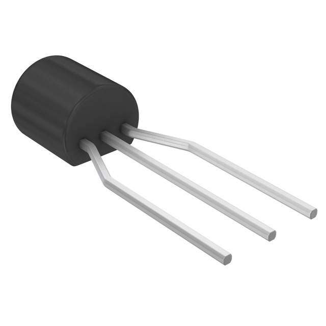
| 描述 | JFET N-CH 35V 350MW TO92JFET 35V 10mA |
| 产品分类 | JFET(结点场效应分离式半导体 |
| FET类型 | N 沟道 |
| 品牌 | ON Semiconductor |
| 产品手册 | |
| 产品图片 |
|
| rohs | 符合RoHS无铅 / 符合限制有害物质指令(RoHS)规范要求 |
| 产品系列 | 晶体管,JFET,ON Semiconductor J112RLRAG- |
| 数据手册 | |
| 产品型号 | J112RLRAG |
| Vgs-Gate-SourceBreakdownVoltage | 35 V |
| Vgs-栅源极击穿电压 | 35 V |
| Vgs=0时的漏-源电流 | 5 mA |
| 不同Id时的电压-截止(VGS关) | 1V @ 1µA |
| 不同Vds(Vgs=0)时的电流-漏极(Idss) | 5mA @ 15V |
| 不同Vds时的输入电容(Ciss) | - |
| 产品种类 | JFET |
| 供应商器件封装 | TO-92-3 |
| 其它名称 | J112RLRAG-ND |
| 功率-最大值 | 350mW |
| 包装 | 带卷 (TR) |
| 商标 | ON Semiconductor |
| 安装类型 | 通孔 |
| 安装风格 | Through Hole |
| 封装 | Reel |
| 封装/外壳 | TO-226-3、TO-92-3(TO-226AA)成形引线 |
| 封装/箱体 | TO-92-3 |
| 工厂包装数量 | 2000 |
| 晶体管极性 | N-Channel |
| 标准包装 | 2,000 |
| 漏极电流(Id)-最大值 | - |
| 漏源极电压(Vdss) | - |
| 电压-击穿(V(BR)GSS) | 35V |
| 电阻-RDS(开) | 50 欧姆 |
| 系列 | J112 |
| 配置 | Single |
| 闸/源击穿电压 | 35 V |

,TO-226_straightlead.jpg)


- 商务部:美国ITC正式对集成电路等产品启动337调查
- 曝三星4nm工艺存在良率问题 高通将骁龙8 Gen1或转产台积电
- 太阳诱电将投资9.5亿元在常州建新厂生产MLCC 预计2023年完工
- 英特尔发布欧洲新工厂建设计划 深化IDM 2.0 战略
- 台积电先进制程称霸业界 有大客户加持明年业绩稳了
- 达到5530亿美元!SIA预计今年全球半导体销售额将创下新高
- 英特尔拟将自动驾驶子公司Mobileye上市 估值或超500亿美元
- 三星加码芯片和SET,合并消费电子和移动部门,撤换高东真等 CEO
- 三星电子宣布重大人事变动 还合并消费电子和移动部门
- 海关总署:前11个月进口集成电路产品价值2.52万亿元 增长14.8%


PDF Datasheet 数据手册内容提取
J111, J112 JFET Chopper Transistors N−Channel — Depletion Features • Pb−Free Packages are Available* http://onsemi.com 1 DRAIN MAXIMUM RATINGS Rating Symbol Value Unit 3 Drain−Gate Voltage VDG −35 Vdc GATE Gate−Source Voltage VGS −35 Vdc Gate Current IG 50 mAdc 2 SOURCE Total Device Dissipation @ TA = 25°C PD 350 mW Derate above = 25°C 2.8 mW/°C Lead Temperature TL 300 °C Operating and Storage Junction TJ, Tstg −65 to +150 °C Temperature Range Maximum ratings are those values beyond which device damage can occur. Maximum ratings applied to the device are individual stress limit values (not TO−92 normal operating conditions) and are not valid simultaneously. If these limits are CASE 29−11 exceeded, device functional operation is not implied, damage may occur and 12 STYLE 5 reliability may be affected. 3 MARKING DIAGRAM J11x AYWW(cid:2) (cid:2) J11x =Device Code x = 1 or 2 A =Assembly Location Y =Year WW =Work Week (cid:2) =Pb−Free Package (Note: Microdot may be in either location) ORDERING INFORMATION See detailed ordering and shipping information in the package dimensions section on page 2 of this data sheet. *For additional information on our Pb−Free strategy and soldering details, please download the ON Semiconductor Soldering and Mounting Techniques Reference Manual, SOLDERRM/D. © Semiconductor Components Industries, LLC, 2006 1 Publication Order Number: March, 2006 − Rev. 2 J111/D
J111, J112 ELECTRICAL CHARACTERISTICS (TA = 25°C unless otherwise noted) Characteristic Symbol Min Max Unit OFF CHARACTERISTICS Gate−Source Breakdown Voltage V(BR)GSS 35 − Vdc (IG = −1.0 (cid:2)Adc) Gate Reverse Current IGSS − −(cid:2)1.0 nAdc (VGS = −15 Vdc) Gate Source Cutoff Voltage VGS(off) Vdc (VDS = 5.0 Vdc, ID = 1.0 (cid:2)Adc) J111 −(cid:2)3.0 −(cid:2)10 J112 −(cid:2)1.0 −(cid:2)5.0 Drain−Cutoff Current ID(off) − 1.0 nAdc (VDS = 5.0 Vdc, VGS = −10 Vdc) ON CHARACTERISTICS Zero−Gate−Voltage Drain Current(1) IDSS mAdc (VDS = 15 Vdc) J111 20 − J112 5.0 − 2.0 − Static Drain−Source On Resistance rDS(on) (cid:3) (VDS = 0.1 Vdc) J111 − 30 J112 − 50 Drain Gate and Source Gate On−Capacitance Cdg(on) − 28 pF (VDS = VGS = 0, f = 1.0 MHz) + Csg(on) Drain Gate Off−Capacitance Cdg(off) − 5.0 pF (VGS = −10 Vdc, f = 1.0 MHz) Source Gate Off−Capacitance Csg(off) − 5.0 pF (VGS = −10 Vdc, f = 1.0 MHz) 1. Pulse Width = 300 (cid:2)s, Duty Cycle = 3.0%. ORDERING INFORMATION Device Package Shipping† J111RL1 TO−92 J111RL1G TO−92 2000 Units / Tape & Reel (Pb−Free) J111RLRA TO−92 J111RLRAG TO−92 2000 Units / Tape & Reel (Pb−Free) J111RLRP TO−92 J111RLRPG TO−92 2000 Units / Tape & Reel (Pb−Free) J112 TO−92 J112G TO−92 1000 Units / Bulk (Pb−Free) J112RL1 TO−92 J112RL1G TO−92 2000 Units / Tape & Reel (Pb−Free) J112RLRA TO−92 J112RLRAG TO−92 2000 Units / Tape & Reel (Pb−Free) †For information on tape and reel specifications, including part orientation and tape sizes, please refer to our Tape and Reel Packaging Specifications Brochure, BRD8011/D. http://onsemi.com 2
J111, J112 TYPICAL SWITCHING CHARACTERISTICS 1000 1000 500 TJ = 25°C 500 TJ = 25°C E (ns) 200 RK = RD′ J111 VGS(off) = 12 V 200 RK = RD′ JJ111112 VGS(off) == 71.02 VV M J112 = 7.0 V J113 = 5.0 V DELAY TI 10500 J113 = 5.0 V ME (ns) 10500 N−ON 20 RISE TI 20 TUR 10 t, r 10 RK = 0 , n) 5.0 RK = 0 5.0 o d( t 2.0 2.0 1.0 1.0 0.5 0.7 1.0 2.0 3.0 5.0 7.0 10 20 30 50 0.5 0.7 1.0 2.0 3.0 5.0 7.0 10 20 30 50 ID, DRAIN CURRENT (mA) ID, DRAIN CURRENT (mA) Figure 1. Turn−On Delay Time Figure 2. Rise Time 1000 1000 TJ = 25°C TJ = 25°C 500 500 ME (ns) 200 JJ111112 VGS(off) == 71.02 VV 200 RK = RD′ JJ111112 VGS(off) == 71.02 VV TI J113 = 5.0 V J113 = 5.0 V AY 100 ns) 100 DEL 50 RK = RD′ ME ( 50 F TI N−OF 20 FALL 20 RK = 0 TUR 10 t, f 10 , off) 5.0 RK = 0 5.0 d( t 2.0 2.0 1.0 1.0 0.5 0.7 1.0 2.0 3.0 5.0 7.0 10 20 30 50 0.5 0.7 1.0 2.0 3.0 5.0 7.0 10 20 30 50 ID, DRAIN CURRENT (mA) ID, DRAIN CURRENT (mA) Figure 3. Turn−Off Delay Time Figure 4. Fall Time NOTE 1 +VDD The switching characteristics shown above were measured using a test circuit similar to Figure 5. At the beginning of the switching interval, RD the gate voltage is at Gate Supply Voltage (−VGG). The Drain−Source SET VDS(off) = 10 V Voltage (VDS) is slightly lower than Drain Supply Voltage (VDD) due INPUT to the voltage divider. Thus Reverse Transfer Capacitance (Crss) or RK RT Gate−Drain Capacitance (Cgd) is charged to VGG + VDS. R50G E(cid:3)N 50 (cid:3) RGG 50 (cid:3) OUTPUT Ddiuscrihnagr getsh eth rotuurgnh− othne sienrtieersv caol,m bGinaateti−oSno oufr cReG eCn aanpdac RitKan. cCeg d (mCugss)t discharge to VDS(on) through RG and RK in series with the parallel VGEN VGG combination of effective load impedance (R′D) and Drain−Source Resistance (rds). During the turn−off, this charge flow is reversed. Predicting turn−on time is somewhat difficult as the channel resistance PULSE WINIDPTUHttTrf P≤≤= U 200L...025S 5 (cid:2)En nsss RGGR (cid:2)D(cid:2) R(cid:3)K RRDD(cid:4)(RTRT(cid:4)(cid:4)505)0 ratudpsrp nirs−o aoa ncfu htniemcst eizo einrs o on fao ntnhd−e l rigdnase tdeae−r.cs Droeuuarrscienes g.v Sotulitnrancg−ee o.C fWfg,d ht hdileies csCihtgausra gdtiieosscn ht hiasrr ogrueevsg,eh Vr srGdesdS, DUTY CYCLE≤ 2.0% with rds increasing as Cgd charges. The above switching curves show two impedance conditions; 1)RK Figure 5. Switching Time Test Circuit is equal to RD, which simulates the switching behavior of cascaded stages where the driving source impedance is normally the load impedance of the previous stage, and 2)RK = 0 (low impedance) the driving source impedance is that of the generator. http://onsemi.com 3
J111, J112 ho 20 15 m m J112 E ( C 10 TTAN 10 J111 F) Cgs DMI J113 E (p 7.0 A C FER 7.0 TAN 5.0 Cgd S CI RAN 5.0 Tchannel = 25°C APA ARD T VDS = 15 V C, C 23..00 T(Cchdasn InSe l N=E 2G5L°CIGIBLE) W 3.0 R O 1.5 F y, fs 2.0 1.0 0.5 0.7 1.0 2.0 3.0 5.0 7.0 10 20 30 50 0.03 0.05 0.1 0.3 0.5 1.0 3.0 5.0 10 30 ID, DRAIN CURRENT (mA) VR, REVERSE VOLTAGE (VOLTS) Figure 6. Typical Forward Transfer Admittance Figure 7. Typical Capacitance 200 2.0 E =ID S1S0 m25A 50(cid:3)mA 75(cid:3)mA 100(cid:3)mA 125(cid:3)mA E 1.8 ID = 1.0 mA TAT 160 mA TATD) VGS = 0 ON−SMS) ON−SALIZE 1.6 , DRAIN−SOURCE s(on)RESISTANCE (OH1284000 Tchannel = 25°C , DRAIN−SOURCE s(on)RESISTANCE (NORM 1101....4280 rd rd 0.6 0 0.4 0 1.0 2.0 3.0 4.0 5.0 6.0 7.0 8.0 −(cid:2)70 −(cid:2)40 −(cid:2)10 20 50 80 110 140 170 VGS, GATE−SOURCE VOLTAGE (VOLTS) Tchannel, CHANNEL TEMPERATURE (°C) Figure 8. Effect of Gate−Source Voltage Figure 9. Effect of Temperature On On Drain−Source Resistance Drain−Source On−State Resistance NOTE 2 E 19000 Tchannel = 25°C 190.0 TS) Tprhien cZipelreo −dGetaetrem−Vinoalntat goe f Dortahienr CJ-uFrEreTn t ch(IaDrSaSc)t,e riiss titchse. T L , DRAIN−SOURCE ON−STAn)RESISTANCE (OHMS) 876543000000 rDS(on) @ VGS = 0 VGS(off) 876543......000000 ATE−SOURCE VOLTAGE (VO FV(oinnrfuiod gFpmtslhut(rooaeebrUrng ede v)ee nir)a1c.x ktlt0aou(nimV neoIsDgswGph SsltoSnhehS(w:e.oo fMswcf )h ntoah asirentna odcrFfet i eltgDharuitersir aotdeii necn1 vs−0vhia.Sc irTpeoish au otiwrisfco iedlGn la sabtO afteo en ww−r iaSiRl tlogh ebiuisvenrie c su±netsa1 epnO0fac%ufreflt rds(o 2100 21..00 V, GGS The elecrdtrs(iocna)l acnhda rVacGtSe rriasntigces tfaobr laen i nJd11ic2ates that an J112 0 0 has an IDSS range of 25 to 75 mA. Figure 10, shows 10 20 30 40 50 60 70 80 90 100110 120 130 140 150 rds(on) = 52 (cid:3) for IDSS = 25 mA and 30 (cid:3) for IDSS, ZERO−GATE−VOLTAGE DRAIN CURRENT (mA) IDSS = 75 mA. The corresponding VGS values are 2.2 V and 4.8 V. Figure 10. Effect of I On Drain−Source DSS Resistance and Gate−Source Voltage http://onsemi.com 4
J111, J112 PACKAGE DIMENSIONS TO−92 (TO−226) CASE 29−11 ISSUE AL A NOTES: B 1. DIMENSIONING AND TOLERANCING PER ANSI Y14.5M, 1982. 2. CONTROLLING DIMENSION: INCH. R 3. CONTOUR OF PACKAGE BEYOND DIMENSION R IS UNCONTROLLED. 4. LEAD DIMENSION IS UNCONTROLLED IN P AND P BEYOND DIMENSION K MINIMUM. L SEATING INCHES MILLIMETERS PLANE K DIM MIN MAX MIN MAX A 0.175 0.205 4.45 5.20 B 0.170 0.210 4.32 5.33 C 0.125 0.165 3.18 4.19 X X D GD 00..001465 00..002515 0.14.0175 0.15.3339 G H 0.095 0.105 2.42 2.66 H J J 0.015 0.020 0.39 0.50 K 0.500 −−− 12.70 −−− V C L 0.250 −−− 6.35 −−− N 0.080 0.105 2.04 2.66 SECTION X−X P −−− 0.100 −−− 2.54 1 N R 0.115 −−− 2.93 −−− V 0.135 −−− 3.43 −−− N STYLE 5: PIN 1. DRAIN 2. SOURCE 3. GATE ON Semiconductor and are registered trademarks of Semiconductor Components Industries, LLC (SCILLC). SCILLC reserves the right to make changes without further notice to any products herein. SCILLC makes no warranty, representation or guarantee regarding the suitability of its products for any particular purpose, nor does SCILLC assume any liability arising out of the application or use of any product or circuit, and specifically disclaims any and all liability, including without limitation special, consequential or incidental damages. “Typical” parameters which may be provided in SCILLC data sheets and/or specifications can and do vary in different applications and actual performance may vary over time. All operating parameters, including “Typicals” must be validated for each customer application by customer’s technical experts. SCILLC does not convey any license under its patent rights nor the rights of others. SCILLC products are not designed, intended, or authorized for use as components in systems intended for surgical implant into the body, or other applications intended to support or sustain life, or for any other application in which the failure of the SCILLC product could create a situation where personal injury or death may occur. Should Buyer purchase or use SCILLC products for any such unintended or unauthorized application, Buyer shall indemnify and hold SCILLC and its officers, employees, subsidiaries, affiliates, and distributors harmless against all claims, costs, damages, and expenses, and reasonable attorney fees arising out of, directly or indirectly, any claim of personal injury or death associated with such unintended or unauthorized use, even if such claim alleges that SCILLC was negligent regarding the design or manufacture of the part. SCILLC is an Equal Opportunity/Affirmative Action Employer. This literature is subject to all applicable copyright laws and is not for resale in any manner. PUBLICATION ORDERING INFORMATION LITERATURE FULFILLMENT: N. American Technical Support: 800−282−9855 Toll Free ON Semiconductor Website: http://onsemi.com Literature Distribution Center for ON Semiconductor USA/Canada P.O. Box 61312, Phoenix, Arizona 85082−1312 USA Order Literature: http://www.onsemi.com/litorder Phone: 480−829−7710 or 800−344−3860 Toll Free USA/Canada Japan: ON Semiconductor, Japan Customer Focus Center Fax: 480−829−7709 or 800−344−3867 Toll Free USA/Canada 2−9−1 Kamimeguro, Meguro−ku, Tokyo, Japan 153−0051 For additional information, please contact your Email: orderlit@onsemi.com Phone: 81−3−5773−3850 local Sales Representative. http://onsemi.com J111/D 5