ICGOO在线商城 > IXXX160N65B4
 Datasheet下载
- 型号: IXXX160N65B4
- 制造商: IXYS
- 库位|库存: xxxx|xxxx
- 要求:
| 数量阶梯 | 香港交货 | 国内含税 |
| +xxxx | $xxxx | ¥xxxx |
查看当月历史价格
查看今年历史价格
IXXX160N65B4产品简介:
ICGOO电子元器件商城为您提供IXXX160N65B4由IXYS设计生产,在icgoo商城现货销售,并且可以通过原厂、代理商等渠道进行代购。 提供IXXX160N65B4价格参考以及IXYSIXXX160N65B4封装/规格参数等产品信息。 你可以下载IXXX160N65B4参考资料、Datasheet数据手册功能说明书, 资料中有IXXX160N65B4详细功能的应用电路图电压和使用方法及教程。
| 参数 | 数值 |
| 25°C时Td(开/关)值 | 52ns/220ns |
| 产品目录 | |
| Current-CollectorPulsed(Icm) | 860A |
| 描述 | IGBT 650V 310A 940W PLUS247IGBT 晶体管 650V/310A TRENCH IGBT GENX4 XPT |
| 产品分类 | IGBT - 单路分离式半导体 |
| GateCharge | 425nC |
| IGBT类型 | PT |
| 品牌 | IXYS |
| 产品手册 | |
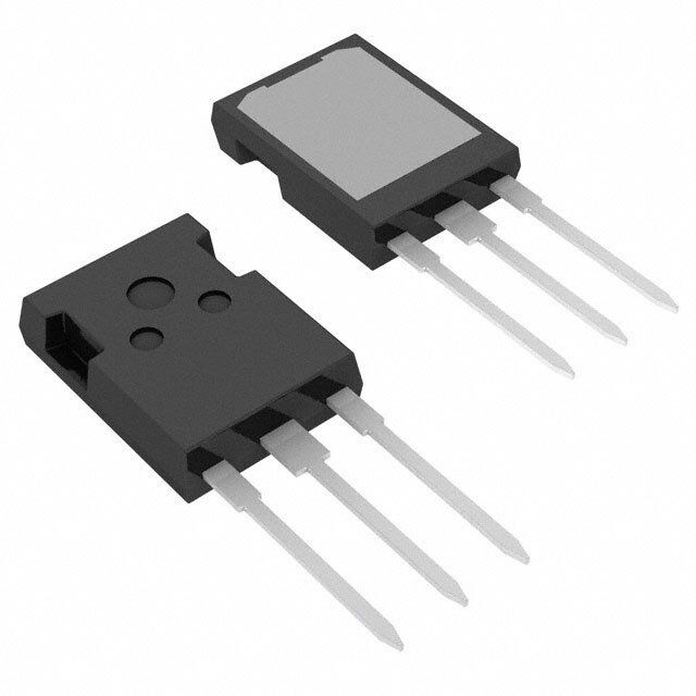
| 产品图片 |
|
| rohs | 符合RoHS无铅 / 符合限制有害物质指令(RoHS)规范要求 |
| 产品系列 | 晶体管,IGBT 晶体管,IXYS IXXX160N65B4GenX4™, XPT™ |
| 数据手册 | |
| 产品型号 | IXXX160N65B4 |
| SwitchingEnergy | 3.3mJ (开), 1.88mJ (关) |
| TestCondition | 400V,80A,1 欧姆,15V |
| 不同 Vge、Ic时的 Vce(on) | 1.8V @ 15V, 160A |
| 产品种类 | IGBT 晶体管 |
| 供应商器件封装 | PLUS247™-3 |
| 功率-最大值 | 940W |
| 功率耗散 | 940 W |
| 包装 | 管件 |
| 反向恢复时间(trr) | - |
| 商标 | IXYS |
| 商标名 | XPT |
| 在25C的连续集电极电流 | 310 A |
| 安装类型 | 通孔 |
| 安装风格 | Through Hole |
| 封装 | Tube |
| 封装/外壳 | TO-247-3 |
| 封装/箱体 | PLUS 247-3 |
| 工厂包装数量 | 30 |
| 最大工作温度 | + 175 C |
| 最小工作温度 | - 55 C |
| 栅极/发射极最大电压 | 20 V |
| 栅极—射极漏泄电流 | 200 nA |
| 标准包装 | 30 |
| 电压-集射极击穿(最大值) | 650V |
| 电流-集电极(Ic)(最大值) | 310A |
| 系列 | IXXX160N65 |
| 输入类型 | 标准 |
| 配置 | Single |
| 集电极—发射极最大电压VCEO | 650 V |
| 集电极—射极饱和电压 | 1.54 V |
| 集电极最大连续电流Ic | 160 A |


- 商务部:美国ITC正式对集成电路等产品启动337调查
- 曝三星4nm工艺存在良率问题 高通将骁龙8 Gen1或转产台积电
- 太阳诱电将投资9.5亿元在常州建新厂生产MLCC 预计2023年完工
- 英特尔发布欧洲新工厂建设计划 深化IDM 2.0 战略
- 台积电先进制程称霸业界 有大客户加持明年业绩稳了
- 达到5530亿美元!SIA预计今年全球半导体销售额将创下新高
- 英特尔拟将自动驾驶子公司Mobileye上市 估值或超500亿美元
- 三星加码芯片和SET,合并消费电子和移动部门,撤换高东真等 CEO
- 三星电子宣布重大人事变动 还合并消费电子和移动部门
- 海关总署:前11个月进口集成电路产品价值2.52万亿元 增长14.8%


PDF Datasheet 数据手册内容提取
Preliminary Technical Information XPTTM 650V IGBTs IXXK160N65B4 V = 650V CES GenX4TM IXXX160N65B4 I = 160A C110 V ≤≤≤≤≤ 1.80V CE(sat) t = 90ns Extreme Light Punch Through fi(typ) IGBT for 10-30kHz Switching TO-264 (IXXK) Symbol Test Conditions Maximum Ratings V T = 25°C to 175°C 650 V G CES J C V T = 25°C to 175°C, R = 1MΩ 650 V E CGR J GE Tab V Continuous ±20 V GES V Transient ±30 V GEM PLUS247 (IXXX) I T = 25°C (Chip Capability) 310 A C25 C I Leads Current Limit 160 A LRMS I T = 110°C 160 A C110 C I T = 25°C, 1ms 860 A CM C SSOA V = 15V, T = 150°C, R = 1Ω I = 320 A G G GE VJ G CM C Tab (RBSOA) Clamped Inductive Load @V ≤ V E CE CES t V = 15V, V = 360V, T = 150°C 10 μs sc GE CE J G = Gate E = Emitter (SCSOA) R = 10Ω, Non Repetitive G C = Collector Tab = Collector P T = 25°C 940 W C C T -55 ... +175 °C J T 175 °C Features JM T -55 ... +175 °C stg (cid:122) Optimized for 10-30kHz Switching T Maximum Lead Temperature for Soldering 300 °C L (cid:122) Square RBSOA T 1.6 mm (0.062in.) from Case for 10s 260 °C SOLD (cid:122) Short Circuit Capability M Mounting Torque (TO-264) 1.13/10 Nm/lb.in. (cid:122) International Standard Packages d (cid:122) High Current Handling Capability F Mounting Force (PLUS247) 20..120 /4.5..27 N/lb. C Weight TO-264 10 g PLUS247 6 g Advantages (cid:122) High Power Density (cid:122) Low Gate Drive Requirement Symbol Test Conditions Characteristic Values Applications (T = 25°C, Unless Otherwise Specified) Min. Typ. Max. J (cid:122) Power Inverters BV I = 250μA, V = 0V 650 V CES C GE (cid:122) UPS V I = 250μA, V = V 4.0 6.5 V (cid:122) Motor Drives GE(th) C CE GE (cid:122) SMPS ICES VCE = VCES, VGE = 0V 25 μA (cid:122) PFC Circuits T = 150°C 1.5 mA (cid:122) Battery Chargers J (cid:122) Welding Machines I V = 0V, V = ±20V ±200 nA GES CE GE (cid:122) Lamp Ballasts V I = 160A, V = 15V, Note 1 1.54 1.80 V CE(sat) C GE T = 150°C 1.85 V J © 2012 IXYS CORPORATION, All Rights Reserved DS100517A(02/13)
IXXK160N65B4 IXXX160N65B4 Symbol Test Conditions Characteristic Values TO-264 Outline (T = 25°C Unless Otherwise Specified) Min. Typ. Max. J g I = 60A, V = 10V, Note 1 40 70 S fs C CE C 8220 pF ies C V = 25V, V = 0V, f = 1MHz 500 pF oes CE GE C 295 pF res Q 425 nC g(on) Q I = 160A, V = 15V, V = 0.5 • V 82 nC ge C GE CE CES Q 193 nC gc t 52 ns d(on) t Inductive load, T = 25°C 64 ns ri J E I = 80A, V = 15V 3.30 mJ on C GE t V = 400V, R = 1Ω 220 ns Terminals: 1 = Gate d(off) CE G 2,4 = Collector t Note 2 90 ns 3 = Emitter fi E 1.88 3.00 mJ off t 43 ns d(on) t Inductive load, T = 150°C 50 ns ri J E I = 80A, V = 15V 4.30 mJ on C GE t V = 400V, R = 1Ω 220 ns d(off) CE G t Note 2 160 ns fi E 2.36 mJ off R 0.16 °C/W thJC R 0.15 °C/W thCS PLUS247TM Outline Notes: 1. Pulse test, t ≤ 300μs, duty cycle, d ≤ 2%. 2. Switching times & energy losses may increase for higher V (clamp), T or R . CE J G Terminals: 1 - Gate 2 - Collector 3 - Emitter Dim. Millimeter Inches PRELIMINARY TECHNICAL INFORMATION Min. Max. Min. Max. The product presented herein is under development. The Technical Specifications offered are derived A 4.83 5.21 .190 .205 A 2.29 2.54 .090 .100 from data gathered during objective characterizations of preliminary engineering lots; but also may yet 1 A 1.91 2.16 .075 .085 contain some information supplied during a pre-production design evaluation. IXYS reserves the right 2 b 1.14 1.40 .045 .055 to change limits, test conditions, and dimensions without notice. b 1.91 2.13 .075 .084 1 b 2.92 3.12 .115 .123 2 C 0.61 0.80 .024 .031 D 20.80 21.34 .819 .840 E 15.75 16.13 .620 .635 e 5.45 BSC .215 BSC L 19.81 20.32 .780 .800 L1 3.81 4.32 .150 .170 Q 5.59 6.20 .220 0.244 R 4.32 4.83 .170 .190 IXYS Reserves the Right to Change Limits, Test Conditions, and Dimensions. IXYS MOSFETs and IGBTs are covered 4,835,592 4,931,844 5,049,961 5,237,481 6,162,665 6,404,065 B1 6,683,344 6,727,585 7,005,734 B2 7,157,338B2 by one or more of the following U.S. patents:4,860,072 5,017,508 5,063,307 5,381,025 6,259,123 B1 6,534,343 6,710,405 B2 6,759,692 7,063,975 B2 4,881,106 5,034,796 5,187,117 5,486,715 6,306,728 B1 6,583,505 6,710,463 6,771,478 B27,071,537
IXXK160N65B4 IXXX160N65B4 Fig. 1. Output Characteristics @ TJ = 25ºC Fig. 2. Extended Output Characteristics @ TJ = 25ºC 320 350 VGE = 15V VGE = 15V 280 13V 300 12V 12V 11V 11V 10V 10V 240 250 s 200 e s per 9V ere200 Am 160 mp 9V I - C 120 - AC150 I 100 80 8V 8V 40 50 7V 0 0 7V 0 0.5 1 1.5 2 2.5 3 0 1 2 3 4 5 6 7 8 9 10 VCE - Volts VCE - Volts Fig. 4. Dependence of V on CE(sat) Fig. 3. Output Characteristics @ T = 150ºC J Junction Temperature 320 2.2 280 V G E = 1153VV 2.0 VGE = 15V 12V 11V 240 1.8 zed I C = 320A peres200 10V ormali 1.6 m160 N 1.4 I - AC120 9V - CE(sat) 1.2 I C = 160A V 80 1.0 8V 40 0.8 7V I C = 80A 0 6V 0.6 0 0.5 1 1.5 2 2.5 3 3.5 4 -50 -25 0 25 50 75 100 125 150 175 VCE - Volts TJ - Degrees Centigrade Fig. 5. Collector-to-Emitter Voltage vs. Fig. 6. Input Admittance Gate-to-Emitter Voltage 4.5 200 4.0 TJ = 25ºC 180 160 3.5 TJ = - 40ºC 140 25ºC V - VoltsCE 223...050 I C = 320A - AmperesC11028000 TJ = 150ºC I 160A 60 1.5 40 1.0 80A 20 0.5 0 7 8 9 10 11 12 13 14 15 4 5 6 7 8 9 10 VGE - Volts VGE - Volts © 2012 IXYS CORPORATION, All Rights Reserved
IXXK160N65B4 IXXX160N65B4 Fig. 7. Transconductance Fig. 8. Gate Charge 120 16 TJ = - 40ºC 14 VCE = 325V 100 I C = 160A 12 I G = 10mA 80 25ºC mens olts 10 e V g - Si f s 60 150ºC V - GE 68 40 4 20 2 0 0 0 20 40 60 80 100 120 140 160 180 200 0 50 100 150 200 250 300 350 400 450 IC - Amperes QG - NanoCoulombs Fig. 9. Capacitance Fig. 10. Reverse-Bias Safe Operating Area 10,000 350 Cies 300 s d ara 250 F o s c e e - Pi1,000 mper200 c A citan Coes I - C150 a p a 100 C TJ = 150ºC f = 1 MHz Cres 50 RdvG /= d t1 Ω< 10V / ns 100 0 0 5 10 15 20 25 30 35 40 100 200 300 400 500 600 700 Fig. 11. Maximum Transient Thermal Impedance VCE - Volts VCE - Volts 1 Fig. 11. Maximum Transient Thermal Impedance 0.3 aaaa 0.1 W C / - ºC Z(th)J 0.01 0.001 0.00001 0.0001 0.001 0.01 0.1 1 10 Pulse Width - Seconds IXYS Reserves the Right to Change Limits, Test Conditions, and Dimensions.
IXXK160N65B4 IXXX160N65B4 Fig. 12. Inductive Switching Energy Loss vs. Fig. 13. Inductive Switching Energy Loss vs. Gate Resistance Collector Current 5.0 9 3.4 7 4.5 Eoff Eon - - - - 8 Eoff Eon - - - - 3.0 6 TJ = 150ºC , VGE = 15V RG = 1Ω , VGE = 15V 4.0 VCE = 400V 7 VCE = 400V 2.6 5 E - MilliJoulesoff2233....0505 I C = 80A 3456onE - MilliJoules E - MilliJoulesoff112...482 TJ = 150ºCTJ = 25ºC 234onE - MilliJoules 1.5 I C = 40A 2 1.0 1 1.0 1 0.5 0 0.6 0 1 2 3 4 5 6 7 8 9 10 40 50 60 70 80 90 100 RG - Ohms IC - Amperes Fig. 14. Inductive Switching Energy Loss vs. Fig. 15. Inductive Turn-off Switching Times vs. Junction Temperature Gate Resistance 2.8 5.5 260 800 2.6 Eoff Eon - - - - 5.0 240 t f i td(off) - - - - 700 2.4 RG = 1Ω , VGE = 15V 4.5 TJ = 150ºC, VGE = 15V VCE = 400V 220 VCE = 400V 600 E - MilliJoulesoff11122.....46802 I C = 80A 22334.....05050onE - MilliJoules t - Nanoseconds f i112680000 I C = 40A I C = 80A 345000000 d(off) - Nanosecondt s 1.2 1.5 I C = 40A 140 200 1.0 1.0 0.8 0.5 120 100 25 50 75 100 125 150 1 2 3 4 5 6 7 8 9 10 TJ - Degrees Centigrade RG - Ohms Fig. 16. Inductive Turn-off Switching Times vs. Fig. 17. Inductive Turn-off Switching Times vs. Collector Current Junction Temperature 300 280 240 340 t f i td(off) - - - - 220 t f i td(off) - - - - 320 280 RG = 1Ω , VGE = 15V 240 RG = 1Ω , VGE = 15V VCE = 400V 200 VCE = 400V 300 t - Nanoseconds f i222246000 TJ = 25ºC TJ = 150ºC 112260000 d(off) - Nanosecondst t - Nanosecondsf i 111110246800000 I IC C == 4800AA 222220246800000 d(off) - Nanosecondst 200 80 80 180 180 40 60 160 40 50 60 70 80 90 100 25 50 75 100 125 150 IC - Amperes TJ - Degrees Centigrade © 2012 IXYS CORPORATION, All Rights Reserved
IXXK160N65B4 IXXX160N65B4 Fig. 18. Inductive Turn-on Switching Times vs. Fig. 19. Inductive Turn-on Switching Times vs. Gate Resistance Collector Current 140 100 100 70 t r i td(on) - - - - 90 t r i td(on) - - - - 65 120 90 TJ = 150ºC, VGE = 15V RG = 1Ω , VGE = 15V VCE = 400V I C = 80A 80 VCE = 400V 60 100 80 t - Nanoseconds r i 468000 I C = 40A 567000 d(on) - Nanosecondst t - Nanosecondsr i 3456700000 TJ = 2T5Jº C= 150ºC 3445550505 d(on)t - Nanoseconds 20 40 20 30 0 30 10 25 1 2 3 4 5 6 7 8 9 10 40 50 60 70 80 90 100 RG - Ohms IC - Amperes Fig. 20. Inductive Turn-on Switching Times vs. Junction Temperature 90 57 80 t r i td(on) - - - - 54 RG = 1Ω , VGE = 15V 70 VCE = 400V 51 ds60 48 dt t - Nanoseconr i 345000 I C = 80A 344925(on) - Nanosecon d 20 I C = 40A 36 s 10 33 0 30 25 50 75 100 125 150 TJ - Degrees Centigrade IXYS Reserves the Right to Change Limits, Test Conditions, and Dimensions. IXYS REF: IXX_160N65B4(E9)12-12-12
Disclaimer Notice - Information furnished is believed to be accurate and reliable. However, users should independently evaluate the suitability of and test each product selected for their own applications. Littelfuse products are not designed for, and may not be used in, all applications. Read complete Disclaimer Notice at www.littelfuse.com/disclaimer-electronics.