 Datasheet下载
- 型号: ISO7420FED
- 制造商: Texas Instruments
- 库位|库存: xxxx|xxxx
- 要求:
| 数量阶梯 | 香港交货 | 国内含税 |
| +xxxx | $xxxx | ¥xxxx |
查看当月历史价格
查看今年历史价格
ISO7420FED产品简介:
ICGOO电子元器件商城为您提供ISO7420FED由Texas Instruments设计生产,在icgoo商城现货销售,并且可以通过原厂、代理商等渠道进行代购。 ISO7420FED价格参考。Texas InstrumentsISO7420FED封装/规格:数字隔离器, 通用 数字隔离器 2500Vrms 2 通道 50Mbps 25kV/µs CMTI 8-SOIC(0.154",3.90mm 宽)。您可以下载ISO7420FED参考资料、Datasheet数据手册功能说明书,资料中有ISO7420FED 详细功能的应用电路图电压和使用方法及教程。
| 参数 | 数值 |
| 产品目录 | |
| ChannelType | 单向 |
| 描述 | DGTL ISO 2.5KV GEN PURP 8SOIC数字隔离器 Low-Power Dual Channel Dig Iso |
| 产品分类 | |
| IsolatedPower | 无 |
| 品牌 | Texas Instruments |
| 产品手册 | |
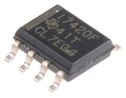
| 产品图片 |
|
| rohs | 符合RoHS无铅 / 符合限制有害物质指令(RoHS)规范要求 |
| 产品系列 | 接口 IC,数字隔离器,Texas Instruments ISO7420FED- |
| 数据手册 | |
| 产品型号 | ISO7420FED |
| PulseWidthDistortion(Max) | 3ns |
| 上升/下降时间(典型值) | 1.8ns, 1.7ns |
| 产品培训模块 | http://www.digikey.cn/PTM/IndividualPTM.page?site=cn&lang=zhs&ptm=26100 |
| 产品种类 | |
| 传播延迟tpLH/tpHL(最大值) | 11ns, 11ns |
| 传播延迟时间 | 7 ns |
| 供应商器件封装 | 8-SOIC |
| 共模瞬态抗扰度(最小值) | 25kV/µs |
| 关闭 | No Shutdown |
| 其它名称 | 296-28105-5 |
| 制造商产品页 | http://www.ti.com/general/docs/suppproductinfo.tsp?distId=10&orderablePartNumber=ISO7420FED |
| 功率耗散 | 138 mW |
| 包装 | 管件 |
| 反向通道 | 0 Channel |
| 商标 | Texas Instruments |
| 安装风格 | SMD/SMT |
| 封装 | Bulk |
| 封装/外壳 | 8-SOIC(0.154",3.90mm 宽) |
| 封装/箱体 | SOIC-8 |
| 工作温度 | -40°C ~ 125°C |
| 工厂包装数量 | 75 |
| 技术 | 容性耦合 |
| 数据速率 | 50Mbps |
| 最大工作温度 | + 125 C |
| 最大数据速率 | 50 Mb/s |
| 最小工作温度 | - 40 C |
| 标准包装 | 75 |
| 正向通道 | 2 Channel |
| 电压-电源 | 3 V ~ 5.5 V |
| 电压-隔离 | 2500Vrms |
| 电源电压-最大 | 5 V |
| 电源电压-最小 | 3.3 V |
| 电源电流 | 6.2 mA |
| 类型 | 通用 |
| 系列 | ISO7420FE |
| 绝缘电压 | 2.5 kVrms |
| 脉宽失真(最大) | 3ns |
| 输入-输入侧1/输入侧2 | 2/0 |
| 通道数 | 2 |
| 通道数量 | 2 Channel |
| 通道类型 | 单向 |
| 隔离式电源 | 无 |


- 商务部:美国ITC正式对集成电路等产品启动337调查
- 曝三星4nm工艺存在良率问题 高通将骁龙8 Gen1或转产台积电
- 太阳诱电将投资9.5亿元在常州建新厂生产MLCC 预计2023年完工
- 英特尔发布欧洲新工厂建设计划 深化IDM 2.0 战略
- 台积电先进制程称霸业界 有大客户加持明年业绩稳了
- 达到5530亿美元!SIA预计今年全球半导体销售额将创下新高
- 英特尔拟将自动驾驶子公司Mobileye上市 估值或超500亿美元
- 三星加码芯片和SET,合并消费电子和移动部门,撤换高东真等 CEO
- 三星电子宣布重大人事变动 还合并消费电子和移动部门
- 海关总署:前11个月进口集成电路产品价值2.52万亿元 增长14.8%


PDF Datasheet 数据手册内容提取
Product Sample & Technical Tools & Support & Folder Buy Documents Software Community ISO7420E,ISO7420FE,ISO7421E,ISO7421FE SLLSE45F–DECEMBER2010–REVISEDJULY2015 ISO742x Low-Power Dual Channel Digital Isolators 1 Features 3 Description • SignalingRate>50Mbps ISO742x provide galvanic isolation up to 2500 VRMS 1 for 1 minute per UL and 4242 V per VDE. These • DefaultOutput'High'and'Low'Options PK devices have two isolated channels. Each channel • LowPowerConsumption:TypicalICCperChannel has a logic input and output buffer separated by a (3.3-VSupplies): silicon dioxide (SiO ) insulation barrier. Used in 2 – ISO7420:1.4mAat1Mbps,2.5mAat conjunction with isolated power supplies, these devices prevent noise currents on a data bus or other 25Mbps circuit from entering the local ground and interfering – ISO7421:1.8mAat1Mbps,2.8mAat with or damaging sensitive circuitry. ISO7420 has 25Mbps both channels in the same direction while ISO7421 • LowPropagationDelay:7nsTypical has the two channels in opposite direction. In case of input power or signal loss, default output is 'low' for • LowPulseSkew:200psTypical devices with suffix 'F' and 'high' for devices without • WideT RangeSpecified:–40°Cto125°C A suffix 'F'. ISO742x have no integrated noise filter and • 50-KV/μsTransientImmunity,Typical thushavefastpropagationdelays. • IsolationBarrierLife: >25Years These devices have TTL input thresholds and • Operatesfrom3-Vto5.5-VSupplyLevels operate from 3-V to 5.5-V supplies. All inputs are 5-V • 3.3-Vand5-VLevelTranslation tolerantwhensuppliedfroma3.3-Vsupply. • NarrowBodySOIC-8Package DeviceInformation(1) • SafetyandRegulatoryApprovals: PARTNUMBER PACKAGE BODYSIZE(NOM) – 4242V IsolationperDINVVDEV0884-10 PK ISO7420E andDINEN61010-1 ISO7420FE – 2500V Isolationfor1minuteperUL1577 SOIC(8) 4.90mmx3.91mm RMS ISO7421E – CSAComponentAcceptanceNotice5A,IEC ISO7421FE 60950-1andIEC61010-1Standards (1) For all available packages, see the orderable addendum at – CQCCertificationperGB4943.1-2011 theendofthedatasheet. – SimplifiedSchematic 2 Applications • Opto-CouplerReplacementin: VCCI VCCO Isolation – IndustrialFieldBus Capacitor – ProfiBus INx OUTx – ModBus – DeviceNet™DataBuses – ServoControlInterface GNDI GNDO – MotorControl V andGNDIaresupplyandground CCI – PowerSupplies connectionsrespectivelyfortheinput channels. – BatteryPacks V andGNDOaresupplyandground CCO connectionsrespectivelyfortheoutput channels. 1 An IMPORTANT NOTICE at the end of this data sheet addresses availability, warranty, changes, use in safety-critical applications, intellectualpropertymattersandotherimportantdisclaimers.PRODUCTIONDATA.
ISO7420E,ISO7420FE,ISO7421E,ISO7421FE SLLSE45F–DECEMBER2010–REVISEDJULY2015 www.ti.com Table of Contents 1 Features.................................................................. 1 10%.......................................................................... 11 2 Applications........................................................... 1 6.14 TypicalCharacteristics..........................................12 3 Description............................................................. 1 7 ParameterMeasurementInformation................15 4 RevisionHistory..................................................... 2 8 DetailedDescription............................................ 16 5 PinConfigurationandFunctions......................... 4 8.1 Overview.................................................................16 8.2 FunctionalBlockDiagram.......................................16 6 Specifications......................................................... 5 8.3 FeatureDescription.................................................17 6.1 AbsoluteMaximumRatings .....................................5 8.4 DeviceFunctionalModes........................................20 6.2 ESDRatings..............................................................5 9 ApplicationsandImplementation...................... 21 6.3 RecommendedOperatingConditions.......................5 6.4 ThermalInformation..................................................5 9.1 ApplicationInformation............................................21 6.5 ElectricalCharacteristics:V andV =5V± 9.2 TypicalApplication .................................................21 CC1 CC2 10%............................................................................ 6 10 PowerSupplyRecommendations..................... 24 6.6 ElectricalCharacteristics:VCC1=5V±10%,VCC2= 11 Layout................................................................... 25 3.3V±10%...............................................................7 11.1 LayoutGuidelines.................................................25 6.7 ElectricalCharacteristics:V =3.3V±10%,V CC1 CC2 11.2 LayoutExample....................................................25 =5V±10%...............................................................8 12 DeviceandDocumentationSupport................. 26 6.8 ElectricalCharacteristics:V andV =3.3V± CC1 CC2 10%............................................................................ 9 12.1 DocumentationSupport........................................26 6.9 PowerDissipationCharacteristics............................9 12.2 RelatedLinks........................................................26 6.10 SwitchingCharacteristics:V andV =5V± 12.3 CommunityResources..........................................26 CC1 CC2 10%.......................................................................... 10 12.4 Trademarks...........................................................26 6.11 SwitchingCharacteristics:V =5V±10%,V 12.5 ElectrostaticDischargeCaution............................26 CC1 CC2 =3.3V±10%..........................................................10 12.6 Glossary................................................................26 6.12 SwitchingCharacteristics:VCC1=3.3V±10%, 13 Mechanical,Packaging,andOrderable V =5V±10%....................................................11 CC2 Information........................................................... 26 6.13 SwitchingCharacteristics:V andV =3.3V± CC1 CC2 4 Revision History NOTE:Pagenumbersforpreviousrevisionsmaydifferfrompagenumbersinthecurrentversion. ChangesfromRevisionE(January2013)toRevisionF Page • ChangedthedatasheetformattothenewTIstandard.......................................................................................................... 1 • AddedPinConfigurationandFunctionssection,ESDRatingstable,FeatureDescriptionsection,DeviceFunctional Modes,ApplicationandImplementationsection,PowerSupplyRecommendationssection,Layoutsection,Device andDocumentationSupportsection,andMechanical,Packaging,andOrderableInformationsection .............................. 1 • DeletedtextfromtheDescription:"CC-gradedeviceshaveintegrated10ns-filtersforharshenvironmentswhere shortnoisepulsesmaybepresentatthedeviceinputpins."................................................................................................ 1 • VDEstandardchangedtoDINVVDEV0884-10(VDEV0884-10):2006-12...................................................................... 1 • DeletedCC-gradefromt ,t intheSwitchingCharacteristicstable.............................................................................. 10 PLH PHL • DeletedCC-gradefromt ,t intheSwitchingCharacteristicstable.............................................................................. 10 PLH PHL • DeletedCC-gradefromt ,t intheSwitchingCharacteristicstable.............................................................................. 11 PLH PHL • DeletedCC-gradefromt ,t intheSwitchingCharacteristicstable.............................................................................. 11 PLH PHL • ChangedtheAvailableOptionsTableTotheFeatureDescriptiontable............................................................................. 17 ChangesfromRevisionD(December2011)toRevisionE Page • DeleteddevicesISO7420FCCandISO7421FCC.................................................................................................................. 1 • ChangedtheNOTE:text...................................................................................................................................................... 17 • AddedtableNotetoV .................................................................................................................................................... 18 IORM • ChangedZtoUndeterminedfortheOUTPUTOUTA,OUTBcolumnoftheFUNCTIONTABLE....................................... 20 2 SubmitDocumentationFeedback Copyright©2010–2015,TexasInstrumentsIncorporated ProductFolderLinks:ISO7420E ISO7420FE ISO7421E ISO7421FE
ISO7420E,ISO7420FE,ISO7421E,ISO7421FE www.ti.com SLLSE45F–DECEMBER2010–REVISEDJULY2015 ChangesfromRevisionC(March2011)toRevisionD Page • ChangedSAFETYfeatureBulletFrom:UL1577Approved;OtherApprovalsPendingTo:AllAgenciesApprovals Completed.............................................................................................................................................................................. 1 • ChangedtheREGULATORYINFORMATIONtable............................................................................................................ 18 ChangesfromRevisionB(January2011)toRevisionC Page • AddeddevicesISO7420FCCandISO7421FCC.................................................................................................................... 1 • ChangedFeaturebulletTo:LowPropagationDelay:7nsTypical(E-Grade)....................................................................... 1 • ChangedFeaturebulletTo:LowPulseSkew:200Typical(E-Grade)................................................................................... 1 • ChangedtheSAFETYandREGULATORYAPPROVALSlist............................................................................................... 1 • ChangedthedatasheetDESCRIPTION................................................................................................................................ 1 • ChangedtheSupplyCurrentvaluesforISO7421xat10,25,and50Mbps.......................................................................... 6 • ChangedtheSupplyCurrentvaluesforISO7421xat10,25,and50Mbps.......................................................................... 7 • ChangedtheSupplyCurrentvaluesforISO7421xat10,25,and50Mbps.......................................................................... 8 • ChangedtheSupplyCurrentvaluesforISO7421x25and50Mbps..................................................................................... 9 • AddedCC-gradeandvaluedtot ,t intheSwitchingCharacteristicstable................................................................. 10 PLH PHL • AddedISO7421xvaluesforPulsewidthdistortion,Channel-to-channeloutputskewtime,andPart-to-partskewtime....10 • AddedCC-gradeandvaluedtot ,t intheSwitchingCharacteristicstable................................................................. 10 PLH PHL • AddedISO7421xvaluesforPulsewidthdistortionandChannel-to-channeloutputskewtime........................................... 10 • AddedCC-gradeandvaluedtot ,t intheSwitchingCharacteristicstable................................................................. 11 PLH PHL • AddedCC-gradeandvaluedtot ,t intheSwitchingCharacteristicstable................................................................. 11 PLH PHL • AddedgraphsFigure5,Figure6,Figure7,andFigure8.................................................................................................... 12 • AddedgraphsFigure14andFigure15................................................................................................................................ 13 • ChangedNote1Figure16................................................................................................................................................... 15 • ChangedFigure17............................................................................................................................................................... 15 • ChangedtheAvailableOptionsTable.................................................................................................................................. 17 • ChangedIsolationresistancetestconditions....................................................................................................................... 17 • ChangedthevaluesofV andV intheINSULATIONCHARACTERISTICStable..................................................... 18 IORM PR • ChangedthevalueofV intheINSULATIONCHARACTERISTICStableFrom:4000To:4242.................................. 18 IOTM • ChangedFigure21............................................................................................................................................................... 19 • ChangedPUtoXinthelastrowoftheFUNCTIONTABLE................................................................................................ 20 • Addedsection:SUPPLYCURRENTEQUATIONS.............................................................................................................. 22 ChangesfromRevisionA(December2010)toRevisionB Page • ChangedFeaturebulletFrom:ISO7421:TBDmAat1Mbps,TBDmAat25MbpsTo:ISO7421:1.8mAat1Mbps, 2.8mAat25Mbps................................................................................................................................................................... 1 • UpdatedtheISO7421xSupplyCurrentvaluesforV andV =5V................................................................................. 6 CC1 CC2 • UpdatedtheISO7421xSupplyCurrentvaluesforV =5VandV =3.3V..................................................................... 7 CC1 CC2 • UpdatedtheISO7421xSupplyCurrentvaluesforV =3.3VandV =5V..................................................................... 8 CC1 CC2 • UpdatedtheISO7421xSupplyCurrentvaluesforV andV =3.3V.............................................................................. 9 CC1 CC2 ChangesfromOriginal(December2010)toRevisionA Page • ChangedtheMaxvaluesforSupplycurrentforV andV ,C =15pF........................................................................... 9 CC1 CC2 L Copyright©2010–2015,TexasInstrumentsIncorporated SubmitDocumentationFeedback 3 ProductFolderLinks:ISO7420E ISO7420FE ISO7421E ISO7421FE
ISO7420E,ISO7420FE,ISO7421E,ISO7421FE SLLSE45F–DECEMBER2010–REVISEDJULY2015 www.ti.com 5 Pin Configuration and Functions ISO7420DPackage 8-PinSOIC ISO7421DPackage TopView 8-PinSOIC TopView VCC1 1 8 VCC2 VCC1 1 8 VCC2 IINNAB 23 olation 76 OOUUTTAB OUTA 2 ation 7 INA Is INB 3 sol 6 OUTB GND1 4 5 GND2 I GND1 4 5 GND2 PinFunctions PIN I/O DESCRIPTION NAME ISO7420x ISO7421x INA 2 7 I Input,channelA INB 3 3 I Input,channelB GND1 4 4 – GroundconnectionforV CC1 GND2 5 5 – GroundconnectionforV CC2 OUTA 7 2 O Output,channelA OUTB 6 6 O Output,channelB V 1 1 – Powersupply,V CC1 CC1 V 8 8 – Powersupply,V CC2 CC2 4 SubmitDocumentationFeedback Copyright©2010–2015,TexasInstrumentsIncorporated ProductFolderLinks:ISO7420E ISO7420FE ISO7421E ISO7421FE
ISO7420E,ISO7420FE,ISO7421E,ISO7421FE www.ti.com SLLSE45F–DECEMBER2010–REVISEDJULY2015 6 Specifications 6.1 Absolute Maximum Ratings(1) MIN MAX UNIT V Supplyvoltage(2),V ,V –0.5 6 V CC CC1 CC2 V VoltageatIN,OUT –0.5 V +0.5(3) V I CC I Outputcurrent ±15 mA O V Maximumsurgeimmunity-SupportsIEC61000-4-5 4000 V SRG PK T Maximumjunctiontemperature 150 °C J(Max) T Storagetemperature –65 150 °C stg (1) StressesbeyondthoselistedunderAbsoluteMaximumRatingsmaycausepermanentdamagetothedevice.Thesearestressratings onlyandfunctionaloperationofthedeviceattheseoranyotherconditionsbeyondthoseindicatedunderrecommendedoperating conditionsisnotimplied.Exposuretoabsolute-maximum-ratedconditionsforextendedperiodsmayaffectdevicereliability. (2) Allvoltagevaluesarewithrespecttonetworkgroundterminalandarepeakvoltagevalues. (3) Maximumvoltagemustnotexceed6V. 6.2 ESD Ratings VALUE UNIT Humanbodymodel(HBM),perANSI/ESDA/JEDECJS-001(1) ±3000 V Electrostaticdischarge Charged-devicemodel(CDM),perJEDECspecificationJESD22-C101(2) ±1500 V (ESD) Machinemodel(MM)ANSI/ESDS5.2-1996 ±200 (1) JEDECdocumentJEP155statesthat500-VHBMallowssafemanufacturingwithastandardESDcontrolprocess. (2) JEDECdocumentJEP157statesthat250-VCDMallowssafemanufacturingwithastandardESDcontrolprocess. 6.3 Recommended Operating Conditions MIN NOM MAX UNIT V ,V Supplyvoltage 3.0 5.5 V CC1 CC2 I High-leveloutputcurrent –4 mA OH I Low-leveloutputcurrent 4 mA OL V High-levelinputvoltage 2 5.5 V IH V Low-levelinputvoltage 0 0.8 V IL t Inputpulseduration 20 ns ui 1/t Signalingrate 0 50(1) Mbps ui T (2) Junctiontemperature –40 136 °C J T AmbientTemperature -40 25 125 °C A (1) Undertypicalconditions,thesedevicesarecapableofsignalingrate>150Mbps. (2) TomaintaintherecommendedoperatingconditionsforT,seetheThermalInformationtable. J 6.4 Thermal Information ISO742x THERMALMETRIC(1) D(SOIC) UNIT 8PINS RθJA Junction-to-ambientthermal Low-Kboard 212 °C/W resistance High-Kboard 116.6 R Junction-to-case(top)thermalresistance 71.6 °C/W θJC(top) R Junction-to-boardthermalresistance 57.3 °C/W θJB ψ Junction-to-topcharacterizationparameter 28.3 °C/W JT ψ Junction-to-boardcharacterizationparameter 56.8 °C/W JB (1) Formoreinformationabouttraditionalandnewthermalmetrics,seetheSemiconductorandICPackageThermalMetricsapplication report,SPRA953. Copyright©2010–2015,TexasInstrumentsIncorporated SubmitDocumentationFeedback 5 ProductFolderLinks:ISO7420E ISO7420FE ISO7421E ISO7421FE
ISO7420E,ISO7420FE,ISO7421E,ISO7421FE SLLSE45F–DECEMBER2010–REVISEDJULY2015 www.ti.com 6.5 Electrical Characteristics: V and V = 5 V ± 10% CC1 CC2 T =–40°Cto125°C A PARAMETER TESTCONDITIONS MIN TYP MAX UNIT IOH=–4mA;seeFigure16. VCCO(1)–0.8 4.6 VOH High-leveloutputvoltage V IOH=–20μA;seeFigure16. VCCO–0.1 5 IOL=4mA;seeFigure16. 0.2 0.4 VOL Low-leveloutputvoltage V IOL=20μA;seeFigure16. 0 0.1 VI(HYS) Inputthresholdvoltagehysteresis 400 mV IIH High-levelinputcurrent INxat0VorVCCI(1) 10 μA IIL Low-levelinputcurrent –10 μA CMTI Common-modetransientimmunity VI=VCCIor0V;seeFigure18. 25 50 kV/μs SUPPLYCURRENT(ALLINPUTSSWITCHINGWITHSQUAREWAVECLOCKSIGNALFORDYNAMICICCMEASUREMENT) ISO7420x ICC1 DCto1Mbps DCInput:VI=VCCIor0V, 0.4 0.8 ICC2 ACInput:CL=15pF 3.4 5 ICC1 0.6 1 10Mbps ICC2 4.5 6 SupplycurrentforVCC1andVCC2 mA ICC1 1 1.5 25Mbps CL=15pF ICC2 6.2 8 ICC1 1.7 2.5 50Mbps ICC2 9 12 ISO7421x ICC1 DCto1Mbps DCInput:VI=VCCIor0V, 2.3 3.6 ICC2 ACInput:CL=15pF 2.3 3.6 ICC1 2.9 4.5 10Mbps ICC2 2.9 4.5 SupplycurrentforVCC1andVCC2 mA ICC1 4.3 6 25Mbps CL=15pF ICC2 4.3 6 ICC1 6 8.5 50Mbps ICC2 6 8.5 (1) V =Input-sideV ;V =Output-sideV CCI CC CCO CC 6 SubmitDocumentationFeedback Copyright©2010–2015,TexasInstrumentsIncorporated ProductFolderLinks:ISO7420E ISO7420FE ISO7421E ISO7421FE
ISO7420E,ISO7420FE,ISO7421E,ISO7421FE www.ti.com SLLSE45F–DECEMBER2010–REVISEDJULY2015 6.6 Electrical Characteristics: V = 5 V ± 10%, V = 3.3 V ± 10% CC1 CC2 T =–40°Cto125°C A PARAMETER TESTCONDITIONS MIN TYP MAX UNIT IOH=–4mA; ISO7421x(5-Vside) VCC1–0.8 4.6 seeFigure16. ISO7420x/7421x(3.3-Vside) VCC2-0.4 3 VOH High-leveloutputvoltage V IOH=–20μA; ISO7421x(5-Vside) VCC1–0.1 5 seeFigure16, ISO7420x/7421x(3.3-Vside) VCC2–0.1 3.3 IOL=4mA;seeFigure16. 0.2 0.4 VOL Low-leveloutputvoltage V IOL=20μA;seeFigure16. 0 0.1 VI(HYS) Inputthresholdvoltagehysteresis 400 mV IIH High-levelinputcurrent 10 μA INxat0VorVCCI IIL Low-levelinputcurrent –10 μA CMTI Common-modetransientimmunity VI=VCCIor0V;seeFigure18. 25 50 kV/μs SUPPLYCURRENT(ALLINPUTSSWITCHINGWITHSQUAREWAVECLOCKSIGNALFORDYNAMICICCMEASUREMENT) ISO7420x ICC1 DCto1Mbps DCInput:VI=VCCIor0V, 0.4 0.8 ICC2 ACInput:CL=15pF 2.6 3.7 ICC1 0.6 1 10Mbps ICC2 3.3 4.3 SupplycurrentforVCC1andVCC2 mA ICC1 1 1.5 25Mbps CL=15pF ICC2 4.4 5.6 ICC1 1.7 2.5 50Mbps ICC2 6.2 7.5 ISO7421x ICC1 DCto1Mbps DCInput:VI=VCCIor0V, 2.3 3.6 ICC2 ACInput:CL=15pF 1.8 2.8 ICC1 2.9 4.5 10Mbps ICC2 2.2 3.2 SupplycurrentforVCC1andVCC2 mA ICC1 4.3 6 25Mbps CL=15pF ICC2 2.8 4.1 ICC1 6 8.5 50Mbps ICC2 3.8 5.5 Copyright©2010–2015,TexasInstrumentsIncorporated SubmitDocumentationFeedback 7 ProductFolderLinks:ISO7420E ISO7420FE ISO7421E ISO7421FE
ISO7420E,ISO7420FE,ISO7421E,ISO7421FE SLLSE45F–DECEMBER2010–REVISEDJULY2015 www.ti.com 6.7 Electrical Characteristics: V = 3.3 V ± 10%, V = 5 V ± 10% CC1 CC2 T =–40°Cto125°C A PARAMETER TESTCONDITIONS MIN TYP MAX UNIT IOH=–4mA;see ISO7421x(3.3-Vside) VCC1–0.4 3 Figure16. ISO7420x/7421x(5-Vside) VCC2–0.8 4.6 VOH High-leveloutputvoltage V IOH=–20μA; ISO7421x(3.3-Vside) VCC1–0.1 3.3 seeFigure16 ISO7420x/7421x(5-Vside) VCC2–0.1 5 IOL=4mA;seeFigure16. 0.2 0.4 VOL Low-leveloutputvoltage V IOL=20μA;seeFigure16. 0 0.1 VI(HYS) Inputthresholdvoltagehysteresis 400 mV IIH High-levelinputcurrent 10 μA INxat0VorVCCI IIL Low-levelinputcurrent –10 μA CMTI Common-modetransientimmunity VI=VCCIor0V;seeFigure18. 25 50 kV/μs SUPPLYCURRENT(ALLINPUTSSWITCHINGWITHSQUAREWAVECLOCKSIGNALFORDYNAMICICCMEASUREMENT) ISO7420x ICC1 DCto1Mbps DCInput:VI=VCCIor0V, 0.2 0.4 ICC2 ACInput:CL=15pF 3.4 5 ICC1 0.4 0.6 10Mbps ICC2 4.5 6 SupplycurrentforVCC1andVCC2 mA ICC1 0.6 0.9 25Mbps CL=15pF ICC2 6.2 8 ICC1 1 1.3 50Mbps ICC2 9 12 ISO7421x ICC1 DCto1Mbps DCInput:VI=VCCIor0V, 1.8 2.8 ICC2 ACInput:CL=15pF 2.3 3.6 ICC1 2.2 3.2 10Mbps ICC2 2.9 4.5 SupplycurrentforVCC2andVCC2 mA ICC1 2.8 4.1 25Mbps CL=15pF ICC2 4.3 6 ICC1 3.8 5.5 50Mbps ICC2 6 8.5 8 SubmitDocumentationFeedback Copyright©2010–2015,TexasInstrumentsIncorporated ProductFolderLinks:ISO7420E ISO7420FE ISO7421E ISO7421FE
ISO7420E,ISO7420FE,ISO7421E,ISO7421FE www.ti.com SLLSE45F–DECEMBER2010–REVISEDJULY2015 6.8 Electrical Characteristics: V and V = 3.3 V ± 10% CC1 CC2 T =–40°Cto125°C A PARAMETER TESTCONDITIONS MIN TYP MAX UNIT IOH=–4mA;seeFigure16. VCCO(1)–0.4 3 VOH High-leveloutputvoltage V IOH=–20μA;seeFigure16. VCCO–0.1 3.3 IOL=4mA;seeFigure16. 0.2 0.4 VOL Low-leveloutputvoltage V IOL=20μA;seeFigure16. 0 0.1 VI(HYS) Inputthresholdvoltagehysteresis 400 mV IIH High-levelinputcurrent INxat0VorVCCI(1) 10 μA IIL Low-levelinputcurrent –10 μA CMTI Common-modetransientimmunity VI=VCCIor0V;seeFigure18. 25 50 kV/μs SUPPLYCURRENT(ALLINPUTSSWITCHINGWITHSQUAREWAVECLOCKSIGNALFORDYNAMICICCMEASUREMENT) ISO7420x ICC1 DCto1Mbps DCInput:VI=VCCIor0V, 0.2 0.4 ICC2 ACInput:CL=15pF 2.6 3.7 ICC1 0.4 0.6 10Mbps ICC2 3.3 4.3 SupplycurrentforVCC1andVCC2 mA ICC1 0.6 0.9 25Mbps CL=15pF ICC2 4.4 5.6 ICC1 1 1.3 50Mbps ICC2 6.2 7.5 ISO7421x ICC1 DCto1Mbps DCInput:VI=VCCIor0V, 1.8 2.8 ICC2 ACInput:CL=15pF 1.8 2.8 ICC1 2.2 3.2 10Mbps ICC2 2.2 3.2 SupplycurrentforVCC2andVCC2 mA ICC1 2.8 4.1 25Mbps CL=15pF ICC2 2.8 4.1 ICC1 3.8 5.5 50Mbps ICC2 3.8 5.5 (1) V =Input-sideV ;V =Output-sideV CCI CC CCO CC 6.9 Power Dissipation Characteristics ISO742x THERMALMETRIC D(SOIC) UNIT 8PINS V =V =5.5V,T =150°C,C =15pF, P Devicepowerdissipation CC1 CC2 J L 138 mW D Inputa100-Mbps50%duty-cyclesquarewave Copyright©2010–2015,TexasInstrumentsIncorporated SubmitDocumentationFeedback 9 ProductFolderLinks:ISO7420E ISO7420FE ISO7421E ISO7421FE
ISO7420E,ISO7420FE,ISO7421E,ISO7421FE SLLSE45F–DECEMBER2010–REVISEDJULY2015 www.ti.com 6.10 Switching Characteristics: V and V = 5 V ± 10% CC1 CC2 T =–40°Cto125°C A PARAMETER TESTCONDITIONS MIN TYP MAX UNIT tPLH,tPHL Propagationdelaytime 7 11 ns ISO7420x SeeFigure16. 0.2 3 PWD(1) Pulsewidthdistortion|tPHL–tPLH| ns ISO7421x 0.3 3.7 ISO7420x 0.3 1 tsk(o)(2) Channel-to-channeloutputskewtime ns ISO7421x 0.3 2 ISO7420x 3.7 tsk(pp)(3) Part-to-partskewtime ns ISO7421x 4.9 tr Outputsignalrisetime 1.8 ns SeeFigure16. tf Outputsignalfalltime 1.7 ns tfs Fail-safeoutputdelaytimefrominputpowerloss SeeFigure17. 6 μs (1) Alsoknownaspulseskew. (2) t istheskewbetweenoutputsofasingledevicewithalldrivinginputsconnectedtogetherandtheoutputsswitchinginthesame sk(o) directionwhiledrivingidenticalloads. (3) t isthemagnitudeofthedifferenceinpropagationdelaytimesbetweenanyterminalsofdifferentdevicesswitchinginthesame sk(pp) directionwhileoperatingatidenticalsupplyvoltages,temperature,inputsignalsandloads. 6.11 Switching Characteristics: V = 5 V ± 10%, V = 3.3 V ± 10% CC1 CC2 T =–40°Cto125°C A PARAMETER TESTCONDITIONS MIN TYP MAX UNIT tPLH,tPHL Propagationdelaytime 8 13.5 ns ISO7420x SeeFigure16. 0.3 3 PWD(1) Pulsewidthdistortion|tPHL–tPLH| ns ISO7421x 0.5 5.6 ISO7420x 1.5 tsk(o)(2) Channel-to-channeloutputskewtime ns ISO7421x 0.5 3 ISO7420x 5.4 tsk(pp)(3) Part-to-partskewtime ns ISO7421x 6.3 tr Outputsignalrisetime 2 ns SeeFigure16. tf Outputsignalfalltime 2 ns tfs Fail-safeoutputdelaytimefrominputpowerloss SeeFigure17. 6 μs (1) Alsoknownaspulseskew. (2) t istheskewbetweenoutputsofasingledevicewithalldrivinginputsconnectedtogetherandtheoutputsswitchinginthesame sk(o) directionwhiledrivingidenticalloads. (3) t isthemagnitudeofthedifferenceinpropagationdelaytimesbetweenanyterminalsofdifferentdevicesswitchinginthesame sk(pp) directionwhileoperatingatidenticalsupplyvoltages,temperature,inputsignalsandloads. 10 SubmitDocumentationFeedback Copyright©2010–2015,TexasInstrumentsIncorporated ProductFolderLinks:ISO7420E ISO7420FE ISO7421E ISO7421FE
ISO7420E,ISO7420FE,ISO7421E,ISO7421FE www.ti.com SLLSE45F–DECEMBER2010–REVISEDJULY2015 6.12 Switching Characteristics: V = 3.3 V ± 10%, V = 5 V ± 10% CC1 CC2 T =–40°Cto125°C A PARAMETER TESTCONDITIONS MIN TYP MAX UNIT ISO7420x 7.5 12 tPLH,tPHL Propagationdelaytime ns ISO7421x 7.5 14 SeeFigure16. ISO7420x 0.7 3 PWD(1) Pulsewidthdistortion|tPHL–tPLH| ns ISO7421x 0.7 3.6 ISO7420x 0.5 1.5 tsk(o)(2) Channel-to-channeloutputskewtime ns ISO7421x 0.5 3 ISO7420x 4.6 tsk(pp)(3) Part-to-partskewtime ns ISO7421x 8.5 tr Outputsignalrisetime 1.7 ns SeeFigure16. tf Outputsignalfalltime 1.6 ns tfs Fail-safeoutputdelaytimefrominputpowerloss SeeFigure17. 6 μs (1) Alsoknownaspulseskew. (2) t istheskewbetweenoutputsofasingledevicewithalldrivinginputsconnectedtogetherandtheoutputsswitchinginthesame sk(o) directionwhiledrivingidenticalloads. (3) t isthemagnitudeofthedifferenceinpropagationdelaytimesbetweenanyterminalsofdifferentdevicesswitchinginthesame sk(pp) directionwhileoperatingatidenticalsupplyvoltages,temperature,inputsignalsandloads. 6.13 Switching Characteristics: V and V = 3.3 V ± 10% CC1 CC2 T =–40°Cto125°C A PARAMETER TESTCONDITIONS MIN TYP MAX UNIT tPLH,tPHL Propagationdelaytime 8.5 14 ns SeeFigure16 PWD(1) Pulsewidthdistortion|tPHL–tPLH| ISO7420xandISO7421x 0.5 2 ns ISO7420x 0.4 2 tsk(o)(2) Channel-to-channeloutputskewtime ns ISO7421x 0.4 3 ISO7420x 6.2 tsk(pp)(3) Part-to-partskewtime ns ISO7421x 6.8 tr Outputsignalrisetime 2 ns SeeFigure16 tf Outputsignalfalltime 1.8 ns tfs Fail-safeoutputdelaytimefrominputpowerloss SeeFigure17 6 μs (1) Alsoknownaspulseskew. (2) t istheskewbetweenoutputsofasingledevicewithalldrivinginputsconnectedtogetherandtheoutputsswitchinginthesame sk(o) directionwhiledrivingidenticalloads. (3) t isthemagnitudeofthedifferenceinpropagationdelaytimesbetweenanyterminalsofdifferentdevicesswitchinginthesame sk(pp) directionwhileoperatingatidenticalsupplyvoltages,temperature,inputsignalsandloads. Copyright©2010–2015,TexasInstrumentsIncorporated SubmitDocumentationFeedback 11 ProductFolderLinks:ISO7420E ISO7420FE ISO7421E ISO7421FE
ISO7420E,ISO7420FE,ISO7421E,ISO7421FE SLLSE45F–DECEMBER2010–REVISEDJULY2015 www.ti.com 6.14 Typical Characteristics 6 12 TA= 25oC TA= 25oC No Load No Load 5 ICC2at 5 V 10 ICC2at 5 V nt - mA 4 ICC2at 3.3 V nt - mA 8 ICC2at 3.3 V urre 3 urre 6 C C ply ply Sup 2 ICC1at 5 V Sup 4 ICC1at 5 V 1 2 ICC1at 3.3 V ICC1at 3.3 V 0 0 0 20 40 60 80 100 120 0 20 40 60 80 100 120 Data Rate - Mbps Data Rate - Mbps Figure1.ISO7420SupplyCurrentPerChannelvsDataRate Figure2.ISO7420SupplyCurrentBothChannelsvsData (NoLoad) Rate(NoLoad) 8 16 TA= 25oC TA= 25oC 7 CL= 15 pF Load ICC2at 5 V 14 CL= 15 pF Load ICC2at 5 V 6 12 Supply Current - mA 345 ICC2at 3.3 V Supply Current - mA 1068 ICC2at 3.3 V 2 ICC1at 5 V 4 ICC1at 5 V 1 2 ICC1at 3.3 V ICC1at 3.3 V 0 0 0 20 40 60 80 100 120 0 20 40 60 80 100 120 Data Rate - Mbps Data Rate - Mbps Figure3.ISO7420SupplyCurrentPerChannelvsDataRate Figure4.ISO7420SupplyCurrentBothChannelsvsData (15pFLoad) Rate(15pFLoad) 4 8 TA= 25oC TA= 25oC No Load No Load 3.5 7 3 6 Current - mA 2.25 ICC1andICC2at 5 V Current - mA 45 ICC1andICC2at 5 V Supply 1.5 ICC1andICC2at 3.3 V Supply 3 ICC1andICC2at 3.3 V 1 2 0.5 1 00 20 40 60 80 100 120 00 20 40 60 80 100 120 Data Rate - Mbps Data Rate - Mbps Figure5.ISO7421SupplyCurrentPerChannelvsDataRate Figure6.ISO7421SupplyCurrentBothChannelsvsData (NoLoad) Rate(NoLoad) 12 SubmitDocumentationFeedback Copyright©2010–2015,TexasInstrumentsIncorporated ProductFolderLinks:ISO7420E ISO7420FE ISO7421E ISO7421FE
ISO7420E,ISO7420FE,ISO7421E,ISO7421FE www.ti.com SLLSE45F–DECEMBER2010–REVISEDJULY2015 Typical Characteristics (continued) 7 10 6 TCAL1=5 2p5FoC 9 TCAL1=5 2p5FoC 8 5 Current - mA 4 ICC1andICC2at 5 V Current - mA 567 ICC1andICC2at 5 V Supply 23 ICC1andICC2at 3.3 V Supply 34 ICC1andICC2at 3.3 V 2 1 1 00 20 40 60 80 100 120 00 20 40 60 80 100 120 Data Rate - Mbps Data Rate - Mbps Figure7.ISO7421SupplyCurrentPerChannelvsDataRate Figure8.ISO7421SupplyCurrentBothChannelsvsData (15pFLoad) Rate(15pFLoad) 8 10.5 VCC1= VCC2= 5 V, VCC1= VCC2= 3.3 V, t- Propagation Delay Time - nspd67..575 CL= 15 pF ttPPLHHL t- Propagation Delay Time - nspd 891..08595 CL= 15 pF tPLtPHHL 6 7.5 -50 -25 0 25 50 75 100 125 150 -50 -25 0 25 50 75 100 125 150 TA- Free-Air Temperature - °C TA- Free-Air Temperature - °C Figure9.PropagationDelayTimevsFree-AirTemperature Figure10.PropagationDelayTimevsFree-AirTemperature 2.7 6 TA= 25°C 2.65 FS+ V 5 Fail-Safe Voltage Threshold - V 22..2245..5556 FS- V- High-Level Output Voltage - OH 1234 Output VCC= 5 V Output VCC= 3.3 V 2.4 0 -50 -25 0 25 50 75 100 125 150 -80 -70 -60 -50 -40 -30 -20 -10 0 TA- Free-Air Temperature - °C IOH- High-Level Output Current - mA Figure11.InputVCCFail-SafeVoltageThresholdvsFree-Air Figure12.High-LevelOutputVoltagevsHigh-LevelOutput Temperature Current Copyright©2010–2015,TexasInstrumentsIncorporated SubmitDocumentationFeedback 13 ProductFolderLinks:ISO7420E ISO7420FE ISO7421E ISO7421FE
ISO7420E,ISO7420FE,ISO7421E,ISO7421FE SLLSE45F–DECEMBER2010–REVISEDJULY2015 www.ti.com Typical Characteristics (continued) 6 1.4 TA= 25°C 1.2 V 5 e - ns ow-Level Output Voltag 234 Output VCC= 3.3 V Output Jitter (PK-PK) - 00..681 OOUUTTAAaanndd O OUUTTBB, ,3 5.3VV-O-Oppeer.r. L 0.4 - OL Output VCC= 5 V V 1 0.2 TA= 25oC CL15 pF 0 0 0 10 20 30 40 50 60 70 0 20 40 60 80 100 120 IOL- Low-Level Output Current - mA Data Rate - Mbps Figure13.Low-LevelOutputVoltagevsLow-LevelOutput Figure14.ISO7420FEOutputJittervsDataRate Current 1.6 1.4 s K) - n 1.2 OUTAand OUTB, 3.3V-Oper. P K- 1 P er ( Jitt 0.8 ut utp 0.6 O OUTAand OUTB, 5V-Oper. 0.4 0.2 TA= 25oC CL15 pF 0 0 20 40 60 80 100 120 Data Rate - Mbps Figure15.ISO7421FEOutputJittervsDataRate 14 SubmitDocumentationFeedback Copyright©2010–2015,TexasInstrumentsIncorporated ProductFolderLinks:ISO7420E ISO7420FE ISO7421E ISO7421FE
ISO7420E,ISO7420FE,ISO7421E,ISO7421FE www.ti.com SLLSE45F–DECEMBER2010–REVISEDJULY2015 7 Parameter Measurement Information IN Barrier OUT VI 1.4 V 1.4 V VCCI n 0 V o GenIneprauttor(1) VI 50W Isolati VO CL(2) tPLH tPHL V V 50% 90% 50% OH O 10% V OL t t r f (1) The input pulse is supplied by a generator having the following characteristics: PRR ≤ 50 kHz, 50% duty cycle, t ≤3ns,t ≤3ns,Z =50Ω.Attheinput,a50-ΩresistorisrequiredtoterminatetheInputGeneratorsignal.Itisnot r f O neededinanactualapplication. (2) C =15pFandincludesinstrumentationandfixturecapacitancewithin±20%. L Figure16. SwitchingCharacteristicTestCircuitandVoltageWaveforms VI VCCI VCCI R RIE VI 2.7V IN =IN 0 = VV (CDCe(vDiceevsic wesit hwoituht ssuuffffiixx FF)) IN TION BAR OUT VO tfs fs high V0OVH ISOLA CL(1) VO 50% fs low VOL (1) C =15pFandincludesinstrumentationandfixturecapacitancewithin±20%. L Figure17. Fail-SafeOutputDelay-TimeTestCircuitandVoltageWaveforms V V CCI CCO C = 0.1μF ±1% C = 0.1μF ±1% Pass-fail criteria– output must remain er stable. arri IN B OUT S1 n atio + sol C (1) V or V I L OH OL – GNDI GNDO + V – CM (1) C =15pFandincludesinstrumentationandfixturecapacitancewithin±20%. L Figure18. Common-ModeTransientImmunityTestCircuit Copyright©2010–2015,TexasInstrumentsIncorporated SubmitDocumentationFeedback 15 ProductFolderLinks:ISO7420E ISO7420FE ISO7421E ISO7421FE
ISO7420E,ISO7420FE,ISO7421E,ISO7421FE SLLSE45F–DECEMBER2010–REVISEDJULY2015 www.ti.com 8 Detailed Description 8.1 Overview The isolator in Figure 19 is based on a capacitive isolation barrier technique. The I/O channel of the device consists of two internal data channels, a high-frequency channel (HF) with a bandwidth from 100 kbps up to 150 Mbps, and a low-frequency channel (LF) covering the range from 100 kbps down to DC. In principle, a single- ended input signal entering the HF-channel is split into a differential signal via the inverter gate at the input. The following capacitor-resistor networks differentiate the signal into transients, which then are converted into differential pulses by two comparators. The comparator outputs drive a NOR-gate flip-flop whose output feeds an output multiplexer. A decision logic (DCL) at the driving output of the flip-flop measures the durations between signal transients. If the duration between two consecutive transients exceeds a certain time limit, (as in the case of a low-frequency signal), the DCL forces the output-multiplexer to switch from the high- to the low- frequencychannel. Because low-frequency input signals require the internal capacitors to assume prohibitively large values, these signals are pulse-width modulated (PWM) with the carrier frequency of an internal oscillator, thus creating a sufficientlyhighfrequencysignal,capableofpassingthecapacitivebarrier.Astheinputismodulated,alow-pass filter (LPF) is needed to remove the high-frequency carrier from the actual data before passing it on to the output multiplexer. 8.2 Functional Block Diagram Figure19. ConceptualBlockDiagramofaDigitalCapacitiveIsolator 16 SubmitDocumentationFeedback Copyright©2010–2015,TexasInstrumentsIncorporated ProductFolderLinks:ISO7420E ISO7420FE ISO7421E ISO7421FE
ISO7420E,ISO7420FE,ISO7421E,ISO7421FE www.ti.com SLLSE45F–DECEMBER2010–REVISEDJULY2015 8.3 Feature Description ISO742x are available in multiple channel configurations and default output state options to enable wide variety ofapplicationuses. PRODUCT DATARATE DEFAULTOUTPUT RATEDT CHANNELDIRECTION A ISO7420E High Same ISO7420FE Low 50Mbps –40°Cto125°C ISO7421E High Opposite ISO7421FE Low 8.3.1 InsulationandSafety-RelatedSpecificationsforD-8Package overrecommendedoperatingconditions(unlessotherwisenoted) PARAMETER TESTCONDITIONS MIN TYP MAX UNIT L(I01) Minimumairgap(clearance) Shortestterminal-to-terminaldistancethroughair 4 mm Minimumexternaltracking Shortestterminal-to-terminaldistanceacrossthe L(I02) 4 mm (creepage) packagesurface Trackingresistance(comparative CTI DINEN60112(VDE0303-11);IEC60112 >400 V trackingindex) Minimuminternalgap(internal Distancethroughtheinsulation 0.014 mm clearance) Isolationresistance,inputto VIO=500V,TA=25°C >1012 Ω RIO output(1) V =500V,100°C≤T ≤max >1011 Ω IO A Barriercapacitance,inputto CIO output(1) VIO=0.4sin(2πft),f=1MHz 1 pF C Inputcapacitance(2) V =V /2+0.4sin(2πft),f=1MHz,V =5V 1 pF I I CC CC (1) Allpinsoneachsideofthebarriertiedtogethercreatingatwo-terminaldevice. (2) Measuredfrominputpintoground. NOTE Creepage and clearance requirements should be applied according to the specific equipment isolation standards of an application. Care should be taken to maintain the creepage and clearance distance of a board design to ensure that the mounting pads of theisolatorontheprinted-circuitboarddonotreducethisdistance. Creepage and clearance on a printed-circuit board become equal in certain cases. Techniques such as inserting grooves and/or ribs on a printed circuit board are used to helpincreasethesespecifications. Copyright©2010–2015,TexasInstrumentsIncorporated SubmitDocumentationFeedback 17 ProductFolderLinks:ISO7420E ISO7420FE ISO7421E ISO7421FE
ISO7420E,ISO7420FE,ISO7421E,ISO7421FE SLLSE45F–DECEMBER2010–REVISEDJULY2015 www.ti.com 8.3.2 InsulationCharacteristics overrecommendedoperatingconditions(unlessotherwisenoted) PARAMETER(1) TESTCONDITIONS SPECIFICATION UNIT DINVVDEV0884-10(VDEV0884-10):2006-12 V Maximumworkingisolationvoltage 566 V IORM PEAK Methoda,Afterenvironmentaltestssubgroup1, V =V x1.6,t=10s, 906 PR IORM PartialDischarge<5pC Methodb1, V Input-to-outputtestvoltage V =V x1.875,t=1s(100%Productiontest) 1062 V PR PR IORM PEAK Partialdischarge<5pC AfterInput/Outputsafetytestsubgroup2/3, V =V x1.2,t=10s, 680 PR IORM Partialdischarge<5pC V =V =4242V TEST IOTM PK V Maximumtransientisolationvoltage t=60sec(qualification) 4242 V IOTM PEAK t=1sec(100%production) R Isolationresistance V =500VatT =150°C >109 Ω S IO S Pollutiondegree 2 UL1577 V =V =2500V ,t=60sec TEST ISO RMS (qualification); V Maximumwithstandisolationvoltage 2500 V ISO V =1.2xV =3000V ,t=1sec(100% RMS TEST ISO RMS production) (1) ClimaticClassification40/125/21 Table1.IEC60664-1RatingsTable PARAMETER TESTCONDITIONS SPECIFICATION Basicisolationgroup Materialgroup II Ratedmainsvoltage≤150V I–IV RMS Installationclassification Ratedmainsvoltage≤300V I–III RMS 8.3.3 RegulatoryInformation VDE CSA UL CQC CertifiedaccordingtoDINV VDEV0884-10(VDEV0884- ApprovedunderCSAComponent RecognizedunderUL1577 CertifiedaccordingtoGB 10):2006-12andDINEN AcceptanceNotice5A,IEC60950-1, ComponentRecognitionProgram 4943.1-2011 61010-1(VDE0411-1):2011- andIEC61010-1 07 2500V IsolationRating; RMS BasicinsulationperCSA60950-1- BasicInsulation; 07+A1andIEC60950-12ndEd+A1, BasicInsulation,Altitude≤ MaximumTransientIsolation 384V maximumworkingvoltage; SingleProtectionIsolationVoltage, 5000m,TropicalClimate,250 Voltage,4242VPK; CSA6R1M0S10-1-04andIEC61010-1 2500V (1) V maximumworking MaximumWorkingIsolation RMS RMS 2ndEd,300V maximumworking voltage Voltage,566V RMS PK voltageforbasicinsulationand150 V forreinforcedinsulation RMS Certificatenumber: Certificatenumber:40016131 Mastercontractnumber:220991 Filenumber:E181974 CQC14001109540 (1) Productiontested≥3000V for1secondinaccordancewithUL1577. RMS 18 SubmitDocumentationFeedback Copyright©2010–2015,TexasInstrumentsIncorporated ProductFolderLinks:ISO7420E ISO7420FE ISO7421E ISO7421FE
ISO7420E,ISO7420FE,ISO7421E,ISO7421FE www.ti.com SLLSE45F–DECEMBER2010–REVISEDJULY2015 8.3.4 LifeExpectancyvsWorkingVoltage 100 s ar e Y – 28Years V at 566 V y IORM c n a ct e p x E e Lif 10 0 120 250 500 750 880 1000 V –Working Voltage–V IORM PK G001 Figure20. LifeExpectancyvsWorkingVoltage 8.3.5 SafetyLimitingValues Safetylimitingintendstopreventpotentialdamagetotheisolationbarrieruponfailureofinputoroutputcircuitry.Afailureof theI/Ocanallowlowresistancetogroundorthesupplyand,withoutcurrentlimiting,dissipatesufficientpowertooverheat thedieanddamagetheisolationbarrier,potentiallyleadingtosecondarysystemfailures. PARAMETER TESTCONDITIONS MIN TYP MAX UNIT Safetyinput,output,orsupply θJA=212°C/W,VI=5.5V,TJ=150°C,TA=25°C 107 I mA S current θ =212°C/W,V =3.6V,T =150°C,T =25°C 164 JA I J A T Maximumsafetytemperature 150 °C S The safety-limiting constraint is the absolute-maximum junction temperature specified in the Absolute Maximum Ratings(1) table. The power dissipation and junction-to-air thermal impedance of the device installed in the application hardware determines the junction temperature. The assumed junction-to-air thermal resistance in the Thermal Information table is that of a device installed in the JESD51-3, Low-Effective-Thermal-Conductivity Test Board for Leaded Surface-Mount Packages and is conservative. The power is the recommended maximum input voltage times the current. The junction temperature is then the ambient temperature plus the power times the junction-to-airthermalresistance. 180 160 mA 140 VCC1,VCC2at 3.6 V − ent 120 urr g C 100 VCC1, VCC2at 5.5 V mitin 80 Li 60 y et af 40 S 20 0 0 50 100 150 200 CaseTemperature−°C Figure21. θ ThermalDeratingCurveperVDE JC (1) StressesbeyondthoselistedunderAbsoluteMaximumRatingsmaycausepermanentdamagetothedevice.Thesearestressratings onlyandfunctionaloperationofthedeviceattheseoranyotherconditionsbeyondthoseindicatedunderrecommendedoperating conditionsisnotimplied.Exposuretoabsolute-maximum-ratedconditionsforextendedperiodsmayaffectdevicereliability. Copyright©2010–2015,TexasInstrumentsIncorporated SubmitDocumentationFeedback 19 ProductFolderLinks:ISO7420E ISO7420FE ISO7421E ISO7421FE
ISO7420E,ISO7420FE,ISO7421E,ISO7421FE SLLSE45F–DECEMBER2010–REVISEDJULY2015 www.ti.com 8.4 Device Functional Modes Table2.FunctionalTable(1) OUTPUT INPUT V V OUTA,OUTB CCI CCO INA,INB ISO7420E/ISO7421E ISO7420FE/ISO7421FE H H H PU PU L L L Open H(2) L(3) PD PU X H(2) L(3) X PD X Undetermined Undetermined (1) V =Input-sideV ;V =Output-sideV ;PU=Poweredup(V ≥3V);PD=Powereddown(V ≤2.1V);X=Irrelevant;H= CCI CC CCO CC CC CC Highlevel;L=Lowlevel; (2) Infail-safecondition,outputdefaultstohighlevel (3) Infail-safecondition,outputdefaultstolowlevel 8.4.1 DeviceI/OSchematic ISO742xE Input V V V CCI CCI CCI 1 MW 500W IN Output V CCO 8W OUT 13W ISO742xFx Input V V CCI CCI 500W IN 1 MW Figure22. DeviceI/OSchematics 20 SubmitDocumentationFeedback Copyright©2010–2015,TexasInstrumentsIncorporated ProductFolderLinks:ISO7420E ISO7420FE ISO7421E ISO7421FE
ISO7420E,ISO7420FE,ISO7421E,ISO7421FE www.ti.com SLLSE45F–DECEMBER2010–REVISEDJULY2015 9 Applications and Implementation NOTE Information in the following applications sections is not part of the TI component specification, and TI does not warrant its accuracy or completeness. TI’s customers are responsible for determining suitability of components for their purposes. Customers should validateandtesttheirdesignimplementationtoconfirmsystemfunctionality. 9.1 Application Information ISO742x utilize single-ended TTL-logic switching technology. Its supply voltage range is from 3 V to 5.5 V for both supplies, V and V . When designing with digital isolators, it is important to keep in mind that due to the CC1 CC2 single-ended design structure, digital isolators do not conform to any specific interface standard and are only intended for isolating single-ended CMOS or TTL digital signal lines. The isolator is typically placed between the data controller (i.e. μC or UART), and a data converter or a line transceiver, regardless of the interface type or standard. 9.2 Typical Application ISO7421 can be used with Texas Instruments' mixed signal micro-controller, digital-to-analog converter, transformerdriver,andvoltageregulatortocreateanisolated4-20mAcurrentloop. V V CC1 CC2 ISO7421 Figure23. Isolated4-20mACurrentLoop Copyright©2010–2015,TexasInstrumentsIncorporated SubmitDocumentationFeedback 21 ProductFolderLinks:ISO7420E ISO7420FE ISO7421E ISO7421FE
ISO7420E,ISO7420FE,ISO7421E,ISO7421FE SLLSE45F–DECEMBER2010–REVISEDJULY2015 www.ti.com Typical Application (continued) 9.2.1 DesignRequirements Unlike optocouplers, which require external components to improve performance, provide bias, or limit current, theISO742xonlyrequiretwoexternalbypasscapacitorstooperate. 9.2.2 DetailedDesignProcedure 9.2.2.1 MaximumSupplyCurrentEquations (CalculatedoverrecommendedoperatingtemperaturerangeandSiliconprocessvariation) 9.2.2.1.1 ISO7420 AtV =V =3.3V ± 10% CC1 CC2 I (max)=I (max)+1.791x10⁻²xf (1) CC1 CC1_Q I (max)=I (max)+1.687x10⁻²xf+3.570x10⁻³xfxC (2) CC2 CC2_Q L AtV =V =5V± 10% CC1 CC2 I (max)=I (max)+3.152x10⁻²xf (3) CC1 CC1_Q I (max)=I (max)+2.709x10⁻²xf+5.365x10⁻³xfxC (4) CC2 CC2_Q L 9.2.2.1.2 ISO7421 AtV =V =3.3V ± 10% CC1 CC2 I (max)=I (max)+1.726x10⁻²xf+1.785x10⁻³xfxC (5) CC1 CC1_Q L I (max)=I (max)+1.726x10⁻²xf+1.785x10⁻³xfxC (6) CC2 CC2_Q L AtV =V =5V± 10% CC1 CC2 I (max)=I (max)+2.920x10⁻²xf+2.682x10⁻³xfxC (7) CC1 CC1_Q L I (max)=I (max)+2.920x10⁻²xf+2.682x10⁻³xfxC (8) CC2 CC2_Q L I (max) and I (max) are equivalent to the maximum supply currents measured in mA under DC input CC1_Q CC2_Q conditions (provided in the specification tables of this data sheet); f is data rate in Mbps of both channels; C is L thecapacitiveloadinpFofbothchannels.I (max)andI (max)aremeasuredinmA. CC1 CC2 9.2.2.2 TypicalSupplyCurrentEquations: (CalculatedoverrecommendedoperatingtemperaturerangeandSiliconprocessvariation) 9.2.2.2.1 ISO7420 AtV =V =3.3V CC1 CC2 I (typ)=I (typ)+1.528x10⁻²xf (9) CC1 CC1_Q I (typ)=I (typ)+1.637x10⁻²xf+3.275x10⁻³xfxC (10) CC2 CC2_Q L AtV =V =5V CC1 CC2 I (typ)=I (typ)+2.640x10⁻²xf (11) CC1 CC1_Q I (typ)=I (typ)+2.502x10⁻²xf+4.919x10⁻³xfxC (12) CC2 CC2_Q L 9.2.2.2.2 ISO7421 AtV =V =3.3V CC1 CC2 I (typ)=I (typ)+1.567x10⁻²xf+1.640x10⁻³xfxC (13) CC1 CC1_Q L I (typ)=I (typ)+1.567x10⁻²xf+1.640x10⁻³xfxC (14) CC2 CC2_Q L AtV =V =5V CC1 CC2 I (typ)=I (typ)+2.550x10⁻²xf+2.416x10⁻³xfxC (15) CC1 CC1_Q L I (typ)=I (typ)+2.550x10⁻²xf+2.461x10⁻³xfxC (16) CC2 CC2_Q L 22 SubmitDocumentationFeedback Copyright©2010–2015,TexasInstrumentsIncorporated ProductFolderLinks:ISO7420E ISO7420FE ISO7421E ISO7421FE
ISO7420E,ISO7420FE,ISO7421E,ISO7421FE www.ti.com SLLSE45F–DECEMBER2010–REVISEDJULY2015 Typical Application (continued) I (typ) and I (typ) are equivalent to the typical supply currents measured in mA under DC input CC1_Q CC2_Q conditions (provided in the specification tables of this data sheet); f is data rate in Mbps of each channel; C is L thecapacitiveloadinpFofeachchannel.I (typ)andI (typ)aremeasuredinmA. CC1 CC2 VCC1 1 8 V CC2 0.1 µF 0.1 µF INA 2 7 OUTA INB 3 6 OUTB GND1 4 5 GND2 Figure24. TypicalISO7420CircuitHookup VCC1 1 8 V CC2 0.1 µF 0.1 µF OUTA 2 7 INA INB 3 6 OUTB GND1 4 5 GND2 Figure25. TypicalISO7421CircuitHookup Copyright©2010–2015,TexasInstrumentsIncorporated SubmitDocumentationFeedback 23 ProductFolderLinks:ISO7420E ISO7420FE ISO7421E ISO7421FE
ISO7420E,ISO7420FE,ISO7421E,ISO7421FE SLLSE45F–DECEMBER2010–REVISEDJULY2015 www.ti.com Typical Application (continued) 9.2.3 ApplicationCurves TA= 25°C, VCC1= VCC2= 3.3 V,Pattern: PRBS 27-1 TA= 25°C, VCC1 = VCC2 = 3.3 V, Pattern: PRBS 27-1 Figure26.ISO7420FETypicalEyeDiagramat50MBPS, Figure27.ISO7420FETypicalEyeDiagramat100MBPS, 3.3VOperation 3.3VOperation 10 Power Supply Recommendations To ensure reliable operation at all data rates and supply voltages, a 0.1 µF bypass capacitor is recommended at input and output supply pins (V and V ). The capacitors should be placed as close to the supply pins as CC1 CC2 possible. If only a single primary-side power supply is available in an application, isolated power can be generated for the secondary-side with the help of a transformer driver such as Texas Instruments' SN6501. For such applications, detailed power supply design and transformer selection recommendations are available in SN6501datasheet(SLLSEA0). 24 SubmitDocumentationFeedback Copyright©2010–2015,TexasInstrumentsIncorporated ProductFolderLinks:ISO7420E ISO7420FE ISO7421E ISO7421FE
ISO7420E,ISO7420FE,ISO7421E,ISO7421FE www.ti.com SLLSE45F–DECEMBER2010–REVISEDJULY2015 11 Layout 11.1 Layout Guidelines AminimumoffourlayersisrequiredtoaccomplishalowEMIPCBdesign(seeFigure28).Layerstackingshould be in the following order (top-to-bottom): high-speed signal layer, ground plane, power plane and low-frequency signallayer. • Routing the high-speed traces on the top layer avoids the use of vias (and the introduction of their inductances) and allows for clean interconnects between the isolator and the transmitter and receiver circuits ofthedatalink. • Placing a solid ground plane next to the high-speed signal layer establishes controlled impedance for transmissionlineinterconnectsandprovidesanexcellentlow-inductancepathforthereturncurrentflow. • Placing the power plane next to the ground plane creates additional high-frequency bypass capacitance of approximately100pF/in2. • Routing the slower speed control signals on the bottom layer allows for greater flexibility as these signal links usuallyhavemargintotoleratediscontinuitiessuchasvias. If an additional supply voltage plane or signal layer is needed, add a second power / ground plane system to the stack to keep it symmetrical. This makes the stack mechanically stable and prevents it from warping. Also the powerandgroundplaneofeachpowersystemcanbeplacedclosertogether,thusincreasingthehigh-frequency bypasscapacitancesignificantly. Fordetailedlayoutrecommendations,seeApplicationNote DigitalIsolatorDesignGuide,SLLA284. 11.1.1 PCBMaterial For digital circuit boards operating below 150 Mbps, (or rise and fall times higher than 1 ns), and trace lengths of up to 10 inches, use standard FR-4 epoxy-glass as PCB material. FR-4 (Flame Retardant 4) meets the requirements of Underwriters Laboratories UL94-V0, and is preferred over cheaper alternatives due to its lower dielectric losses at high frequencies, less moisture absorption, greater strength and stiffness, and its self- extinguishingflammability-characteristics. 11.2 Layout Example High-speed traces 10 mils Ground plane Keep this space free FR-4 40 mils from planes, 0r~ 4.5 traces, pads, and vias Power plane 10 mils Low-speed traces Figure28. RecommendedLayerStack Copyright©2010–2015,TexasInstrumentsIncorporated SubmitDocumentationFeedback 25 ProductFolderLinks:ISO7420E ISO7420FE ISO7421E ISO7421FE
ISO7420E,ISO7420FE,ISO7421E,ISO7421FE SLLSE45F–DECEMBER2010–REVISEDJULY2015 www.ti.com 12 Device and Documentation Support 12.1 Documentation Support 12.1.1 RelatedDocumentation Forrelateddocumentationseethefollowing: • SN6501TransformerDriverforIsolatedPowerSupplies,SLLSEA0 • IsolationGlossary,SLLS353 12.2 Related Links The table below lists quick access links. Categories include technical documents, support and community resources,toolsandsoftware,andquickaccesstosampleorbuy. Table3.RelatedLinks TECHNICAL TOOLS& SUPPORT& PARTS PRODUCTFOLDER SAMPLE&BUY DOCUMENTS SOFTWARE COMMUNITY ISO7420E Clickhere Clickhere Clickhere Clickhere Clickhere ISO7420FE Clickhere Clickhere Clickhere Clickhere Clickhere ISO7421E Clickhere Clickhere Clickhere Clickhere Clickhere ISO7421FE Clickhere Clickhere Clickhere Clickhere Clickhere 12.3 Community Resources The following links connect to TI community resources. Linked contents are provided "AS IS" by the respective contributors. They do not constitute TI specifications and do not necessarily reflect TI's views; see TI's Terms of Use. TIE2E™OnlineCommunity TI'sEngineer-to-Engineer(E2E)Community.Createdtofostercollaboration amongengineers.Ate2e.ti.com,youcanaskquestions,shareknowledge,exploreideasandhelp solveproblemswithfellowengineers. DesignSupport TI'sDesignSupport QuicklyfindhelpfulE2Eforumsalongwithdesignsupporttoolsand contactinformationfortechnicalsupport. 12.4 Trademarks DeviceNet,E2EaretrademarksofTexasInstruments. Allothertrademarksarethepropertyoftheirrespectiveowners. 12.5 Electrostatic Discharge Caution Thesedeviceshavelimitedbuilt-inESDprotection.Theleadsshouldbeshortedtogetherorthedeviceplacedinconductivefoam duringstorageorhandlingtopreventelectrostaticdamagetotheMOSgates. 12.6 Glossary SLYZ022—TIGlossary. Thisglossarylistsandexplainsterms,acronyms,anddefinitions. 13 Mechanical, Packaging, and Orderable Information The following pages include mechanical, packaging, and orderable information. This information is the most current data available for the designated devices. This data is subject to change without notice and revision of thisdocument.Forbrowser-basedversionsofthisdatasheet,refertotheleft-handnavigation. 26 SubmitDocumentationFeedback Copyright©2010–2015,TexasInstrumentsIncorporated ProductFolderLinks:ISO7420E ISO7420FE ISO7421E ISO7421FE
PACKAGE OPTION ADDENDUM www.ti.com 21-May-2013 PACKAGING INFORMATION Orderable Device Status Package Type Package Pins Package Eco Plan Lead/Ball Finish MSL Peak Temp Op Temp (°C) Device Marking Samples (1) Drawing Qty (2) (3) (4/5) ISO7420ED ACTIVE SOIC D 8 75 Green (RoHS CU NIPDAU Level-1-260C-UNLIM -40 to 125 SO7420 & no Sb/Br) ISO7420EDR ACTIVE SOIC D 8 2500 Green (RoHS CU NIPDAU Level-1-260C-UNLIM -40 to 125 SO7420 & no Sb/Br) ISO7420FED ACTIVE SOIC D 8 75 Green (RoHS CU NIPDAU Level-1-260C-UNLIM -40 to 125 I7420F & no Sb/Br) ISO7420FEDR ACTIVE SOIC D 8 2500 Green (RoHS CU NIPDAU Level-1-260C-UNLIM -40 to 125 I7420F & no Sb/Br) ISO7421ED ACTIVE SOIC D 8 75 Green (RoHS CU NIPDAU Level-1-260C-UNLIM -40 to 125 SO7421 & no Sb/Br) ISO7421EDR ACTIVE SOIC D 8 2500 Green (RoHS CU NIPDAU Level-1-260C-UNLIM -40 to 125 SO7421 & no Sb/Br) ISO7421FED ACTIVE SOIC D 8 75 Green (RoHS CU NIPDAU Level-1-260C-UNLIM -40 to 125 I7421F & no Sb/Br) ISO7421FEDR ACTIVE SOIC D 8 2500 Green (RoHS CU NIPDAU Level-1-260C-UNLIM -40 to 125 I7421F & no Sb/Br) (1) The marketing status values are defined as follows: ACTIVE: Product device recommended for new designs. LIFEBUY: TI has announced that the device will be discontinued, and a lifetime-buy period is in effect. NRND: Not recommended for new designs. Device is in production to support existing customers, but TI does not recommend using this part in a new design. PREVIEW: Device has been announced but is not in production. Samples may or may not be available. OBSOLETE: TI has discontinued the production of the device. (2) Eco Plan - The planned eco-friendly classification: Pb-Free (RoHS), Pb-Free (RoHS Exempt), or Green (RoHS & no Sb/Br) - please check http://www.ti.com/productcontent for the latest availability information and additional product content details. TBD: The Pb-Free/Green conversion plan has not been defined. Pb-Free (RoHS): TI's terms "Lead-Free" or "Pb-Free" mean semiconductor products that are compatible with the current RoHS requirements for all 6 substances, including the requirement that lead not exceed 0.1% by weight in homogeneous materials. Where designed to be soldered at high temperatures, TI Pb-Free products are suitable for use in specified lead-free processes. Pb-Free (RoHS Exempt): This component has a RoHS exemption for either 1) lead-based flip-chip solder bumps used between the die and package, or 2) lead-based die adhesive used between the die and leadframe. The component is otherwise considered Pb-Free (RoHS compatible) as defined above. Green (RoHS & no Sb/Br): TI defines "Green" to mean Pb-Free (RoHS compatible), and free of Bromine (Br) and Antimony (Sb) based flame retardants (Br or Sb do not exceed 0.1% by weight in homogeneous material) (3) MSL, Peak Temp. -- The Moisture Sensitivity Level rating according to the JEDEC industry standard classifications, and peak solder temperature. Addendum-Page 1
PACKAGE OPTION ADDENDUM www.ti.com 21-May-2013 (4) There may be additional marking, which relates to the logo, the lot trace code information, or the environmental category on the device. (5) Multiple Device Markings will be inside parentheses. Only one Device Marking contained in parentheses and separated by a "~" will appear on a device. If a line is indented then it is a continuation of the previous line and the two combined represent the entire Device Marking for that device. Important Information and Disclaimer:The information provided on this page represents TI's knowledge and belief as of the date that it is provided. TI bases its knowledge and belief on information provided by third parties, and makes no representation or warranty as to the accuracy of such information. Efforts are underway to better integrate information from third parties. TI has taken and continues to take reasonable steps to provide representative and accurate information but may not have conducted destructive testing or chemical analysis on incoming materials and chemicals. TI and TI suppliers consider certain information to be proprietary, and thus CAS numbers and other limited information may not be available for release. In no event shall TI's liability arising out of such information exceed the total purchase price of the TI part(s) at issue in this document sold by TI to Customer on an annual basis. OTHER QUALIFIED VERSIONS OF ISO7421E : •Automotive: ISO7421E-Q1 NOTE: Qualified Version Definitions: •Automotive - Q100 devices qualified for high-reliability automotive applications targeting zero defects Addendum-Page 2
PACKAGE MATERIALS INFORMATION www.ti.com 26-Feb-2019 TAPE AND REEL INFORMATION *Alldimensionsarenominal Device Package Package Pins SPQ Reel Reel A0 B0 K0 P1 W Pin1 Type Drawing Diameter Width (mm) (mm) (mm) (mm) (mm) Quadrant (mm) W1(mm) ISO7420EDR SOIC D 8 2500 330.0 12.4 6.4 5.2 2.1 8.0 12.0 Q1 ISO7420FEDR SOIC D 8 2500 330.0 12.4 6.4 5.2 2.1 8.0 12.0 Q1 ISO7421EDR SOIC D 8 2500 330.0 12.4 6.4 5.2 2.1 8.0 12.0 Q1 ISO7421FEDR SOIC D 8 2500 330.0 12.4 6.4 5.2 2.1 8.0 12.0 Q1 PackMaterials-Page1
PACKAGE MATERIALS INFORMATION www.ti.com 26-Feb-2019 *Alldimensionsarenominal Device PackageType PackageDrawing Pins SPQ Length(mm) Width(mm) Height(mm) ISO7420EDR SOIC D 8 2500 350.0 350.0 43.0 ISO7420FEDR SOIC D 8 2500 350.0 350.0 43.0 ISO7421EDR SOIC D 8 2500 350.0 350.0 43.0 ISO7421FEDR SOIC D 8 2500 350.0 350.0 43.0 PackMaterials-Page2
PACKAGE OUTLINE D0008A SOIC - 1.75 mm max height SCALE 2.800 SMALL OUTLINE INTEGRATED CIRCUIT C SEATING PLANE .228-.244 TYP [5.80-6.19] .004 [0.1] C A PIN 1 ID AREA 6X .050 [1.27] 8 1 2X .189-.197 [4.81-5.00] .150 NOTE 3 [3.81] 4X (0 -15 ) 4 5 8X .012-.020 B .150-.157 [0.31-0.51] .069 MAX [3.81-3.98] .010 [0.25] C A B [1.75] NOTE 4 .005-.010 TYP [0.13-0.25] 4X (0 -15 ) SEE DETAIL A .010 [0.25] .004-.010 0 - 8 [0.11-0.25] .016-.050 [0.41-1.27] DETAIL A (.041) TYPICAL [1.04] 4214825/C 02/2019 NOTES: 1. Linear dimensions are in inches [millimeters]. Dimensions in parenthesis are for reference only. Controlling dimensions are in inches. Dimensioning and tolerancing per ASME Y14.5M. 2. This drawing is subject to change without notice. 3. This dimension does not include mold flash, protrusions, or gate burrs. Mold flash, protrusions, or gate burrs shall not exceed .006 [0.15] per side. 4. This dimension does not include interlead flash. 5. Reference JEDEC registration MS-012, variation AA. www.ti.com
EXAMPLE BOARD LAYOUT D0008A SOIC - 1.75 mm max height SMALL OUTLINE INTEGRATED CIRCUIT 8X (.061 ) [1.55] SYMM SEE DETAILS 1 8 8X (.024) [0.6] SYMM (R.002 ) TYP [0.05] 5 4 6X (.050 ) [1.27] (.213) [5.4] LAND PATTERN EXAMPLE EXPOSED METAL SHOWN SCALE:8X SOLDER MASK SOLDER MASK METAL OPENING OPENING METAL UNDER SOLDER MASK EXPOSED METAL EXPOSED METAL .0028 MAX .0028 MIN [0.07] [0.07] ALL AROUND ALL AROUND NON SOLDER MASK SOLDER MASK DEFINED DEFINED SOLDER MASK DETAILS 4214825/C 02/2019 NOTES: (continued) 6. Publication IPC-7351 may have alternate designs. 7. Solder mask tolerances between and around signal pads can vary based on board fabrication site. www.ti.com
EXAMPLE STENCIL DESIGN D0008A SOIC - 1.75 mm max height SMALL OUTLINE INTEGRATED CIRCUIT 8X (.061 ) [1.55] SYMM 1 8 8X (.024) [0.6] SYMM (R.002 ) TYP [0.05] 5 4 6X (.050 ) [1.27] (.213) [5.4] SOLDER PASTE EXAMPLE BASED ON .005 INCH [0.125 MM] THICK STENCIL SCALE:8X 4214825/C 02/2019 NOTES: (continued) 8. Laser cutting apertures with trapezoidal walls and rounded corners may offer better paste release. IPC-7525 may have alternate design recommendations. 9. Board assembly site may have different recommendations for stencil design. www.ti.com
IMPORTANTNOTICEANDDISCLAIMER TIPROVIDESTECHNICALANDRELIABILITYDATA(INCLUDINGDATASHEETS),DESIGNRESOURCES(INCLUDINGREFERENCE DESIGNS),APPLICATIONOROTHERDESIGNADVICE,WEBTOOLS,SAFETYINFORMATION,ANDOTHERRESOURCES“ASIS” ANDWITHALLFAULTS,ANDDISCLAIMSALLWARRANTIES,EXPRESSANDIMPLIED,INCLUDINGWITHOUTLIMITATIONANY IMPLIEDWARRANTIESOFMERCHANTABILITY,FITNESSFORAPARTICULARPURPOSEORNON-INFRINGEMENTOFTHIRD PARTYINTELLECTUALPROPERTYRIGHTS. TheseresourcesareintendedforskilleddevelopersdesigningwithTIproducts.Youaresolelyresponsiblefor(1)selectingtheappropriate TIproductsforyourapplication,(2)designing,validatingandtestingyourapplication,and(3)ensuringyourapplicationmeetsapplicable standards,andanyothersafety,security,orotherrequirements.Theseresourcesaresubjecttochangewithoutnotice.TIgrantsyou permissiontousetheseresourcesonlyfordevelopmentofanapplicationthatusestheTIproductsdescribedintheresource.Other reproductionanddisplayoftheseresourcesisprohibited.NolicenseisgrantedtoanyotherTIintellectualpropertyrightortoanythird partyintellectualpropertyright.TIdisclaimsresponsibilityfor,andyouwillfullyindemnifyTIanditsrepresentativesagainst,anyclaims, damages,costs,losses,andliabilitiesarisingoutofyouruseoftheseresources. TI’sproductsareprovidedsubjecttoTI’sTermsofSale(www.ti.com/legal/termsofsale.html)orotherapplicabletermsavailableeitheron ti.comorprovidedinconjunctionwithsuchTIproducts.TI’sprovisionoftheseresourcesdoesnotexpandorotherwisealterTI’sapplicable warrantiesorwarrantydisclaimersforTIproducts. MailingAddress:TexasInstruments,PostOfficeBox655303,Dallas,Texas75265 Copyright©2019,TexasInstrumentsIncorporated