ICGOO在线商城 > 分立半导体产品 > 二极管 - 整流器 - 单 > ISL9R30120G2
 Datasheet下载
- 型号: ISL9R30120G2
- 制造商: Fairchild Semiconductor
- 库位|库存: xxxx|xxxx
- 要求:
| 数量阶梯 | 香港交货 | 国内含税 |
| +xxxx | $xxxx | ¥xxxx |
查看当月历史价格
查看今年历史价格
ISL9R30120G2产品简介:
ICGOO电子元器件商城为您提供ISL9R30120G2由Fairchild Semiconductor设计生产,在icgoo商城现货销售,并且可以通过原厂、代理商等渠道进行代购。 ISL9R30120G2价格参考¥5.50-¥5.50。Fairchild SemiconductorISL9R30120G2封装/规格:二极管 - 整流器 - 单, 标准 通孔 二极管 1200V 30A TO-247-2。您可以下载ISL9R30120G2参考资料、Datasheet数据手册功能说明书,资料中有ISL9R30120G2 详细功能的应用电路图电压和使用方法及教程。
ISL9R30120G2 是一款由 ON Semiconductor 提供的高效整流二极管,属于二极管 - 整流器 - 单类别。其主要应用场景包括以下领域:

 1. 电源管理
   - DC-DC 转换器:在开关模式电源(SMPS)中作为续流二极管,用于提高效率并减少能量损耗。
   - AC-DC 转换器:在桥式整流电路中,将交流电转换为直流电,适用于各种家用电器和工业设备。

 2. 汽车电子
   - 车载充电系统:用于车载逆变器或充电模块,支持高效的电力传输。
   - 发电机整流:在汽车发电机中,将产生的交流电转换为直流电,为电池充电。
   - LED 驱动器:在车灯系统中,确保电流单向流动,保护电路免受反向电压的影响。

 3. 工业应用
   - 电机驱动:在工业电机控制中,作为整流元件,提供稳定的直流电源。
   - 太阳能逆变器:在光伏系统中,用于将太阳能电池板产生的直流电转换为交流电,同时保护电路免受反向电流损害。
   - 不间断电源(UPS):在 UPS 系统中,用于整流和保护电池充电电路。

 4. 消费电子
   - 笔记本适配器:在电源适配器中,用于将市电转换为适合设备使用的直流电。
   - 电视和显示器:在电源模块中,用于整流功能,确保稳定的电源供应。

 5. 通信设备
   - 基站电源:在通信基站中,用于高效的电力转换和保护电路。
   - 路由器和交换机:在电源模块中,提供稳定可靠的直流输出。

 特性优势
- 低正向压降:降低功耗,提高系统效率。
- 高浪涌能力:能够承受瞬时大电流,增强可靠性。
- 快速恢复时间:适合高频应用,减少开关损耗。

总之,ISL9R30120G2 的高性能和可靠性使其成为多种电力转换和保护场景的理想选择,广泛应用于汽车、工业、消费电子和通信领域。
| 参数 | 数值 |
| 产品目录 | |
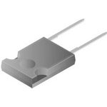
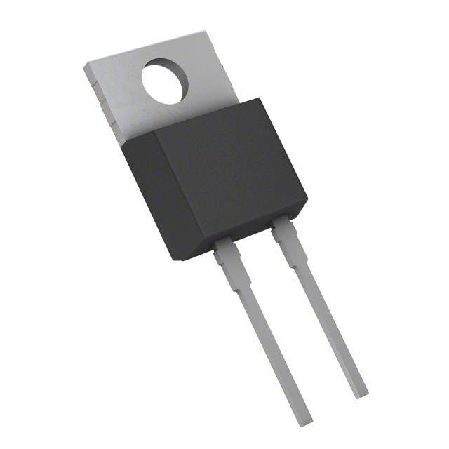
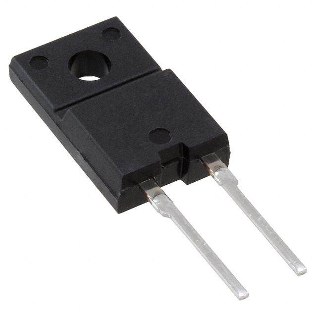
| 描述 | DIODE FAST REC 1.2KV 30A TO247二极管 - 通用,功率,开关 30A 1200V STEALTH |
| 产品分类 | 单二极管/整流器分离式半导体 |
| 品牌 | Fairchild Semiconductor |
| 产品手册 | |
| 产品图片 |
|
| rohs | 符合RoHS无铅 / 符合限制有害物质指令(RoHS)规范要求 |
| 产品系列 | 二极管与整流器,二极管 - 通用,功率,开关,Fairchild Semiconductor ISL9R30120G2Stealth™ |
| 数据手册 | |
| 产品型号 | ISL9R30120G2 |
| PCN设计/规格 | |
| 不同If时的电压-正向(Vf) | 3.3V @ 30A |
| 不同 Vr、F时的电容 | - |
| 不同 Vr时的电流-反向漏电流 | 100µA @ 1200V |
| 二极管类型 | 标准 |
| 产品种类 | 二极管 - 通用,功率,开关 |
| 供应商器件封装 | TO-247 |
| 其它名称 | ISL9R30120G2-ND |
| 包装 | 管件 |
| 单位重量 | 6.330 g |
| 反向恢复时间(trr) | 100ns |
| 商标 | Fairchild Semiconductor |
| 安装类型 | 通孔,径向 |
| 安装风格 | Through Hole |
| 封装 | Tube |
| 封装/外壳 | TO-247-2 |
| 封装/箱体 | TO-247 |
| 峰值反向电压 | 1200 V |
| 工作温度-结 | -55°C ~ 150°C |
| 工厂包装数量 | 30 |
| 恢复时间 | 100 ns |
| 最大反向漏泄电流 | 1000 uA |
| 最大工作温度 | + 150 C |
| 最大浪涌电流 | 325 A |
| 最小工作温度 | - 55 C |
| 标准包装 | 30 |
| 正向电压下降 | 3.3 V |
| 正向连续电流 | 30 A |
| 热阻 | 1°C/W Jc |
| 电压-DC反向(Vr)(最大值) | 1200V(1.2kV) |
| 电流-平均整流(Io) | 30A |
| 系列 | ISL9R30120 |
| 速度 | 快速恢复 =< 500 ns,> 200mA(Io) |
| 配置 | Single |
| 零件号别名 | ISL9R30120G2_NL |


- 商务部:美国ITC正式对集成电路等产品启动337调查
- 曝三星4nm工艺存在良率问题 高通将骁龙8 Gen1或转产台积电
- 太阳诱电将投资9.5亿元在常州建新厂生产MLCC 预计2023年完工
- 英特尔发布欧洲新工厂建设计划 深化IDM 2.0 战略
- 台积电先进制程称霸业界 有大客户加持明年业绩稳了
- 达到5530亿美元!SIA预计今年全球半导体销售额将创下新高
- 英特尔拟将自动驾驶子公司Mobileye上市 估值或超500亿美元
- 三星加码芯片和SET,合并消费电子和移动部门,撤换高东真等 CEO
- 三星电子宣布重大人事变动 还合并消费电子和移动部门
- 海关总署:前11个月进口集成电路产品价值2.52万亿元 增长14.8%


PDF Datasheet 数据手册内容提取
Is Now Part of To learn more about ON Semiconductor, please visit our website at www.onsemi.com Please note: As part of the Fairchild Semiconductor integration, some of the Fairchild orderable part numbers will need to change in order to meet ON Semiconductor’s system requirements. Since the ON Semiconductor product management systems do not have the ability to manage part nomenclature that utilizes an underscore (_), the underscore (_) in the Fairchild part numbers will be changed to a dash (-). This document may contain device numbers with an underscore (_). Please check the ON Semiconductor website to verify the updated device numbers. The most current and up-to-date ordering information can be found at www.onsemi.com. Please email any questions regarding the system integration to Fairchild_questions@onsemi.com. ON Semiconductor and the ON Semiconductor logo are trademarks of Semiconductor Components Industries, LLC dba ON Semiconductor or its subsidiaries in the United States and/or other countries. ON Semiconductor owns the rights to a number of patents, trademarks, copyrights, trade secrets, and other intellectual property. A listing of ON Semiconductor’s product/patent coverage may be accessed at www.onsemi.com/site/pdf/Patent-Marking.pdf. ON Semiconductor reserves the right to make changes without further notice to any products herein. ON Semiconductor makes no warranty, representation or guarantee regarding the suitability of its products for any particular purpose, nor does ON Semiconductor assume any liability arising out of the application or use of any product or circuit, and specifically disclaims any and all liability, including without limitation special, consequential or incidental damages. Buyer is responsible for its products and applications using ON Semiconductor products, including compliance with all laws, regulations and safety requirements or standards, regardless of any support or applications information provided by ON Semiconductor. “Typical” parameters which may be provided in ON Semiconductor data sheets and/or specifications can and do vary in different applications and actual performance may vary over time. All operating parameters, including “Typicals” must be validated for each customer application by customer’s technical experts. ON Semiconductor does not convey any license under its patent rights nor the rights of others. ON Semiconductor products are not designed, intended, or authorized for use as a critical component in life support systems or any FDA Class 3 medical devices or medical devices with a same or similar classification in a foreign jurisdiction or any devices intended for implantation in the human body. Should Buyer purchase or use ON Semiconductor products for any such unintended or unauthorized application, Buyer shall indemnify and hold ON Semiconductor and its officers, employees, subsidiaries, affiliates, and distributors harmless against all claims, costs, damages, and expenses, and reasonable attorney fees arising out of, directly or indirectly, any claim of personal injury or death associated with such unintended or unauthorized use, even if such claim alleges that ON Semiconductor was negligent regarding the design or manufacture of the part. ON Semiconductor is an Equal Opportunity/Affirmative Action Employer. This literature is subject to all applicable copyright laws and is not for resale in any manner.
I S L 9 February 2014 R 3 0 ISL9R30120G2 1 2 0 G 30 A, 1200 V STEALTH™ Diode 2 Features Description — •Stealth Recovery trr = 269 ns (@ IF = 30 A) The ISL9R30120G2 is a STEALTH™ diode optimized for S low loss performance in high frequency hard switched T •Max Forward Voltage, VF = 3.3 V (@ TC = 25°C) applications. The STEALTH™ family exhibits low reverse E A •1200 V Reverse Voltage and High Reliability recovery current (IRR) and exceptionally soft recovery under L typical operating conditions. This device is intended for use •Avalanche Energy Rated T as a free wheeling or boost diode in power supplies and H •RoHS Compliant other power switching applications. The low IRR and short ta ™ phase reduce loss in switching transistors. The soft recovery minimizes ringing, expanding the range of D conditions under which the diode may be operated without i Applications the use of additional snubber circuitry. Consider using the o (cid:127) Switch Mode Power Supplies STEALTH™ diode with an SMPS IGBT to provide the most d efficient and highest power density design at lower cost. e (cid:127) Hard Switched PFC Boost Diode (cid:127) UPS Free Wheeling Diode (cid:127) Motor Drive FWD (cid:127) SMPS FWD • Snubber Diode Package Symbol JEDEC STYLE 2 LEAD TO-247 ANODE CATHODE K CATHODE (BOTTOM SIDE METAL) A Device Maximum Ratings TC = 25°C unless otherwise noted Symbol Parameter Rating Unit V Repetitive Peak Reverse Voltage 1200 V RRM V Working Peak Reverse Voltage 1200 V RWM V DC Blocking Voltage 1200 V R I Average Rectified Forward Current (T = 80oC) 30 A F(AV) C IFRM Repetitive Peak Surge Current (20 kHz Square Wave) 70 A IFSM Nonrepetitive Peak Surge Current (Halfwave 1 Phase 60 Hz) 325 A P Power Dissipation 166 W D EAVL Avalanche Energy (1 A, 40 mH) 20 mJ T , T Operating and Storage Temperature Range -55 to 175 °C J STG TL Maximum Temperature for Soldering 300 °C TPKG Leads at 0.063 in (1.6 mm) from Case for 10 s 260 °C Package Body for 10s, See Application Note AN-7528 CAUTION: Stresses above those listed in “Absolute Maximum Ratings” may cause permanent damage to the device. This is a stress only rating and operation of the device at these or any other conditions above those indicated in the operational sections of this specification is not implied. ©2002 Fairchild Semiconductor 1 www.fairchildsemi.com Corporation ISL9R30120G2 Rev. C2
I S Package Marking and Ordering Information L 9 Part Number Top Mark Package Packing Method Tape Width Quantity R ISL9R30120G2 R30120G2 TO-247 Tube N/A 30 3 0 1 Electrical Characteristics TC = 25°C unless otherwise noted 2 0 Symbol Parameter Test Conditions Min Typ Max Unit G 2 Off State Characteristics — IR Instantaneous Reverse Current VR = 1200 V TC = 25°C - - 100 µA T = 125°C - - 1.0 mA S C T E On State Characteristics A VF Instantaneous Forward Voltage IF = 30 A TC = 25°C - 2.8 3.3 V L T = 125°C - 2.6 3.1 V T C H Dynamic Characteristics ™ CJ Junction Capacitance VR = 10 V, IF = 0 A - 115 - pF D i o Switching Characteristics d trr Reverse Recovery Time IF = 1 A, dI/dt = 100 A/µs, VR = 15 V - 45 56 ns e IF = 30 A, dI/dt = 100 A/µs, VR = 15 V - 80 100 ns trr Reverse Recovery Time IF = 30 A, - 269 - ns I Reverse Recovery Current dIF/dt = 200 A/µs, - 7.5 - A rr Q Reverse Recovered Charge VR = 780 V, TC = 25°C - 930 - nC rr trr Reverse Recovery Time IF = 30 A, - 529 - ns S Softness Factor (tb/ta) dIF/dt = 200 A/µs, - 6.2 - - I Reverse Recovery Current VR = 780 V, - 11 - A rr T = 125°C C Q Reverse Recovered Charge - 3.0 - µC rr trr Reverse Recovery Time IF = 30 A, - 260 - ns S Softness Factor (tb/ta) dIF/dt = 1000 A/µs, - 4.8 - - I Reverse Recovery Current VR = 780 V, - 30 - A rr T = 125°C C Q Reverse Recovered Charge - 3.4 - µC rr dI /dt Maximum di/dt during t - 520 - A/µs M b Thermal Characteristics RθJC Thermal Resistance Junction to Case TO-247 - - 0.75 °C/W RθJA Thermal Resistance Junction to Ambient TO-247 - - 30 °C/W ©2002 Fairchild Semiconductor Corporation 2 www.fairchildsemi.com ISL9R30120G2 Rev. C2
I S Typical Performance Curves L 9 R 60 1000 150oC 3 0 D CURRENT (A) 345000 125oC 150oC E CURRENT (µA) 11000 11 720550oooCCC 120G2 — R S I, FORWAF 1200 25oC 100oC I, REVERR 0.11 25oC STEA L T 0 0.01 0.5 1 1.5 2 2.5 3 3.5 4 0.2 0.3 0.4 0.5 0.6 0.7 0.8 0.9 1.0 1.1 1.2 H ™ VF, FORWARD VOLTAGE (V) VR, REVERSE VOLTAGE (KV) Figure 1. Forward Current vs Forward Voltage Figure 2. Reverse Current vs Reverse Voltage D i o d 750 750 VR = 780V, TC = 125oC VR = 780V, TC = 125oC e 625 625 MES (ns) 500 tb at dIF/dt = 200A/µs, 500A/µs, 800A/µs MES (ns) 500 tb at IF = 60A, 30A, 15A RY TI 375 RY TI 375 OVE OVE REC 250 REC 250 t, t, 125 ta at dIF/dt = 200A/µs, 500A/µs, 800A/µs 125 ta at IF = 60A, 30A, 15A 0 0 0 10 20 30 40 50 60 200 400 600 800 1000 1200 IF, FORWARD CURRENT (A) dIF/dt, CURRENT RATE OF CHANGE (A/µs) Figure 3. t and t Curves vs Forward Current Figure 4. t and t Curves vs dI /dt a b a b F 40 40 A) VR = 780V, TC = 125oC A) VR = 780V, TC = 125oC NT ( NT ( 35 E E RR 30 dIF/dt = 800A/µs RR U U C C 30 ERY dIF/dt = 500A/µs ERY V V O 20 O 25 REC REC IF = 60A SE dIF/dt = 200A/µs SE 20 VER 10 VER IF = 30A E E AX R AX R 15 IF = 15A M M I, RR 00 10 20 30 40 50 60 I, RR 10200 400 600 800 1000 1200 IF, FORWARD CURRENT (A) dIF/dt, CURRENT RATE OF CHANGE (A/µs) Figure 5. Maximum Reverse Recovery Current vs Figure 6. Maximum Reverse Recovery Current vs Forward Current dI /dt F ©2002 Fairchild Semiconductor Corporation 3 www.fairchildsemi.com ISL9R30120G2 Rev. C2
I S Typical Performance Curves (Continued) L 9 R 9 6.0 FACTOR 8 VR = 780V, TC = 125oC GE (µC) 5.6 VR = 780V, TC = 125oC IF = 60A 301 S R 2 ES IF = 60A HA 5.0 0 OFTN 7 ED C 4.5 G RY S 6 OVER 4.0 2 — RECOVE 5 IF = 30A SE REC 3.5 IF = 30A S EVERSE 4 IF = 15A , REVERR 23..50 IF = 15A TEA R R L S, 3 Q 2.0 T 200 400 600 800 1000 1200 200 400 600 800 1000 1200 H dIF/dt, CURRENT RATE OF CHANGE (A/µs) dIF/dt, CURRENT RATE OF CHANGE (A/µs) ™ Figure 7. Reverse Recovery Softness Factor vs Figure 8. Reverse Recovery Charge vs dI /dt D F dI /dt i F o d 1600 f = 1MHZ NT (A) -14 IF = 30A, VR = 780V, dIF/dt = 500A/µs 400 e CITANCE (pF)111024000000 OVERY CURRE -16 IRM(REC) 350 MES (ns) C, JUNCTION CAPAJ 246800000000 , MAX REVERSE RECC) --2108 tRR 235000 t, RECOVERY TI E R 0 RM( -22 200 0.03 0.1 1 10 100 I 25 50 75 100 125 150 VR, REVERSE VOLTAGE (V) TC, CASE TEMPERATURE (oC) Figure 9. Junction Capacitance vs Reverse Voltage Figure 10. Maximum Reverse Recovery Current and trr vs Case Temperature 80 ]A [V) A F( 60 nt, I e urr C d 40 r a w or F ge 20 a r e v A 0 25 50 75 100 125 150 175 Case temperature, T [oC] C Figure 11. DC Current Derating Curve ©2002 Fairchild Semiconductor Corporation 4 www.fairchildsemi.com ISL9R30120G2 Rev. C2
I Typical Performance Curves (Continued) S L 9 R DUTY CYCLE - DESCENDING ORDER 3 0.5 0 1.0 0.2 1 E 0.1 2 D C 0.05 0 ZE AN 0.02 G ORMALI L IMPED 0.01 PDM 2 — Z,N θJAHERMA 0.1 t1t2 ST T NOTES: E SINGLE PULSE DPEUATKY TFAJ C= TPODMR :x D Z θ=J tA1 /xt2 RθJA + TA AL T 0.01 H 10-5 10-4 10-3 10-2 10-1 100 101 ™ t, RECTANGULAR PULSE DURATION (s) D Figure 12. Normalized Maximum Transient Thermal Impedance io d e Test Circuit and Waveforms VGE AMPLITUDE AND RG CONTROL dIF/dt L t1 AND t2 CONTROL IF IF ddItF ta trr tb DUT CURRENT 0 RG SENSE + VGE t1 MOSFET -VDD 0IR.2M5 IRM t2 Figure 13. trr Test Circuit Figure 14. trr Waveforms and Definitions I = 1A L = 40mH R < 0.1Ω VDD = 50V EAVL = 1/2LI2 [VR(AVL)/(VR(AVL) - VDD)] Q1 = IGBT (BVCES > DUT VR(AVL)) L R VAVL CURRENT + SENSE VDD IL IL Q1 I V VDD DUT - t0 t1 t2 t Figure 15. Avalanche Energy Test Circuit Figure 16. Avalanche Current and Voltage Waveforms ©2002 Fairchild Semiconductor Corporation 5 www.fairchildsemi.com ISL9R30120G2 Rev. C2
I S Mechanical Dimensions L 9 R 3 TO-247 2L 0 1 2 0 G 2 — S T E A L T H ™ D i o d e Figure 17. TO-247,Molded, 2LD, Jedec Option AB Package drawings are provided as a service to customers considering Fairchild components. Drawings may change in any manner without notice. Please note the revision and/or date on the drawing and contact a Fairchild Semiconductor representative to verify or obtain the most recent revision. Package specifications do not expand the terms of Fairchild’s worldwide terms and conditions, specif- ically the warranty therein, which covers Fairchild products. Always visit Fairchild Semiconductor’s online packaging area for the most recent package drawings: http://www.fairchildsemi.com/package/packageDetails.html?id=PN_TO247-002. ©2002 Fairchild Semiconductor Corporation 6 www.fairchildsemi.com ISL9R30120G2 Rev. C2
I S L 9 R 3 0 1 TRADEMARKS 2 The following includes registered and unregistered trademarks and service marks, owned by Fairchild Semiconductor and/or its global subsidiaries, and is not 0 G intended to be an exhaustive list of all such trademarks. 2 AccuPower™ F-PFS™ Sync-Lock™ AX-CAP®* FRFET® ® ®* — BitSiC™ Global Power ResourceSM PowerTrench® Build it Now™ GreenBridge™ PowerXS™ TinyBoost® S CCoorreePPOLUWSE™R™ GGrreeeenn FFPPSS™™ e-Series™ PQrFoEgTra®mmable Active Droop™ TinyBuck® T TinyCalc™ E CROSSVOLT™ Gmax™ QS™ TinyLogic® A CTL™ GTO™ Quiet Series™ Current Transfer Logic™ IntelliMAX™ RapidConfigure™ TINYOPTO™ L DEUXPEED® ISOPLANAR™ ™ TinyPower™ T TinyPWM™ Dual Cool™ Marking Small Speakers Sound Louder H EcoSPARK® and Better™ Saving our world, 1mW/W/kW at a time™ TTirnaynWSiiCre™™ ™ EfficentMax™ MegaBuck™ SignalWise™ TriFault Detect™ ESBC™ MICROCOUPLER™ SmartMax™ TRUECURRENT®* D MicroFET™ SMART START™ ® MicroPak™ Solutions for Your Success™ SerDes™ io Fairchild® MicroPak2™ SPM® d FFAaiCrcTh iQldu Sieet mSiecroiensd™uctor® MMiollteiorDnMrivaex™™ SSuTpEeArLFTEHT™® UHC® e FACT® mWSaver® SuperSOT™-3 Ultra FRFET™ FAST® OptoHiT™ SuperSOT™-6 UniFET™ FastvCore™ OPTOLOGIC® SuperSOT™-8 VCX™ FETBench™ OPTOPLANAR® SupreMOS® VisualMax™ FPS™ SyncFET™ VoltagePlus™ XS™ *Trademarks of System General Corporation, used under license by Fairchild Semiconductor. DISCLAIMER FAIRCHILD SEMICONDUCTOR RESERVES THE RIGHT TO MAKE CHANGES WITHOUT FURTHER NOTICE TO ANY PRODUCTS HEREIN TO IMPROVE RELIABILITY, FUNCTION, OR DESIGN. FAIRCHILD DOES NOT ASSUME ANY LIABILITY ARISING OUT OF THE APPLICATION OR USE OF ANY PRODUCT OR CIRCUIT DESCRIBED HEREIN; NEITHER DOES IT CONVEY ANY LICENSE UNDER ITS PATENT RIGHTS, NOR THE RIGHTS OF OTHERS. THESE SPECIFICATIONS DO NOT EXPAND THE TERMS OF FAIRCHILD’S WORLDWIDE TERMS AND CONDITIONS, SPECIFICALLY THE WARRANTY THEREIN, WHICH COVERS THESE PRODUCTS. LIFE SUPPORT POLICY FAIRCHILD’S PRODUCTS ARE NOT AUTHORIZED FOR USE AS CRITICAL COMPONENTS IN LIFE SUPPORT DEVICES OR SYSTEMS WITHOUT THE EXPRESS WRITTEN APPROVAL OF FAIRCHILD SEMICONDUCTOR CORPORATION. As used here in: 1. Life support devices or systems are devices or systems which, (a) are 2. A critical component in any component of a life support, device, or intended for surgical implant into the body or (b) support or sustain life, system whose failure to perform can be reasonably expected to cause and (c) whose failure to perform when properly used in accordance with the failure of the life support device or system, or to affect its safety or instructions for use provided in the labeling, can be reasonably effectiveness. expected to result in a significant injury of the user. ANTI-COUNTERFEITING POLICY Fairchild Semiconductor Corporation’s Anti-Counterfeiting Policy. Fairchild’s Anti-Counterfeiting Policy is also stated on our external website, www.Fairchildsemi.com, under Sales Support. Counterfeiting of semiconductor parts is a growing problem in the industry. All manufactures of semiconductor products are experiencing counterfeiting of their parts. Customers who inadvertently purchase counterfeit parts experience many problems such as loss of brand reputation, substandard performance, failed application, and increased cost of production and manufacturing delays. Fairchild is taking strong measures to protect ourselves and our customers from the proliferation of counterfeit parts. Fairchild strongly encourages customers to purchase Fairchild parts either directly from Fairchild or from Authorized Fairchild Distributors who are listed by country on our web page cited above. Products customers buy either from Fairchild directly or from Authorized Fairchild Distributors are genuine parts, have full traceability, meet Fairchild’s quality standards for handing and storage and provide access to Fairchild’s full range of up-to-date technical and product information. Fairchild and our Authorized Distributors will stand behind all warranties and will appropriately address and warranty issues that may arise. Fairchild will not provide any warranty coverage or other assistance for parts bought from Unauthorized Sources. Fairchild is committed to combat this global problem and encourage our customers to do their part in stopping this practice by buying direct or from authorized distributors. PRODUCT STATUS DEFINITIONS Definition of Terms Datasheet Identification Product Status Definition Datasheet contains the design specifications for product development. Specifications Advance Information Formative / In Design may change in any manner without notice. Datasheet contains preliminary data; supplementary data will be published at a later Preliminary First Production date. Fairchild Semiconductor reserves the right to make changes at any time without notice to improve design. Datasheet contains final specifications. Fairchild Semiconductor reserves the right to No Identification Needed Full Production make changes at any time without notice to improve the design. Datasheet contains specifications on a product that is discontinued by Fairchild Obsolete Not In Production Semiconductor. The datasheet is for reference information only. Rev. I66 ©2002 Fairchild Semiconductor Corporation 7 www.fairchildsemi.com ISL9R30120G2 Rev. C2
ON Semiconductor and are trademarks of Semiconductor Components Industries, LLC dba ON Semiconductor or its subsidiaries in the United States and/or other countries. ON Semiconductor owns the rights to a number of patents, trademarks, copyrights, trade secrets, and other intellectual property. A listing of ON Semiconductor’s product/patent coverage may be accessed at www.onsemi.com/site/pdf/Patent−Marking.pdf. ON Semiconductor reserves the right to make changes without further notice to any products herein. ON Semiconductor makes no warranty, representation or guarantee regarding the suitability of its products for any particular purpose, nor does ON Semiconductor assume any liability arising out of the application or use of any product or circuit, and specifically disclaims any and all liability, including without limitation special, consequential or incidental damages. Buyer is responsible for its products and applications using ON Semiconductor products, including compliance with all laws, regulations and safety requirements or standards, regardless of any support or applications information provided by ON Semiconductor. “Typical” parameters which may be provided in ON Semiconductor data sheets and/or specifications can and do vary in different applications and actual performance may vary over time. All operating parameters, including “Typicals” must be validated for each customer application by customer’s technical experts. ON Semiconductor does not convey any license under its patent rights nor the rights of others. ON Semiconductor products are not designed, intended, or authorized for use as a critical component in life support systems or any FDA Class 3 medical devices or medical devices with a same or similar classification in a foreign jurisdiction or any devices intended for implantation in the human body. Should Buyer purchase or use ON Semiconductor products for any such unintended or unauthorized application, Buyer shall indemnify and hold ON Semiconductor and its officers, employees, subsidiaries, affiliates, and distributors harmless against all claims, costs, damages, and expenses, and reasonable attorney fees arising out of, directly or indirectly, any claim of personal injury or death associated with such unintended or unauthorized use, even if such claim alleges that ON Semiconductor was negligent regarding the design or manufacture of the part. ON Semiconductor is an Equal Opportunity/Affirmative Action Employer. This literature is subject to all applicable copyright laws and is not for resale in any manner. PUBLICATION ORDERING INFORMATION LITERATURE FULFILLMENT: N. American Technical Support: 800−282−9855 Toll Free ON Semiconductor Website: www.onsemi.com Literature Distribution Center for ON Semiconductor USA/Canada 19521 E. 32nd Pkwy, Aurora, Colorado 80011 USA Europe, Middle East and Africa Technical Support: Order Literature: http://www.onsemi.com/orderlit Phone: 303−675−2175 or 800−344−3860 Toll Free USA/Canada Phone: 421 33 790 2910 Fax: 303−675−2176 or 800−344−3867 Toll Free USA/Canada Japan Customer Focus Center For additional information, please contact your local Email: orderlit@onsemi.com Phone: 81−3−5817−1050 Sales Representative © Semiconductor Components Industries, LLC www.onsemi.com www.onsemi.com 1
Mouser Electronics Authorized Distributor Click to View Pricing, Inventory, Delivery & Lifecycle Information: O N Semiconductor: ISL9R30120G2