ICGOO在线商城 > 集成电路(IC) > 线性 - 音頻放大器 > ISL99201IRTCZ-TK

 Datasheet下载
- 型号: ISL99201IRTCZ-TK
- 制造商: Intersil
- 库位|库存: xxxx|xxxx
- 要求:
| 数量阶梯 | 香港交货 | 国内含税 |
| +xxxx | $xxxx | ¥xxxx |
查看当月历史价格
查看今年历史价格
ISL99201IRTCZ-TK产品简介:
ICGOO电子元器件商城为您提供ISL99201IRTCZ-TK由Intersil设计生产,在icgoo商城现货销售,并且可以通过原厂、代理商等渠道进行代购。 ISL99201IRTCZ-TK价格参考。IntersilISL99201IRTCZ-TK封装/规格:线性 - 音頻放大器, Amplifier IC 1-通道(单声道) D 类 8-TDFN(3x3)。您可以下载ISL99201IRTCZ-TK参考资料、Datasheet数据手册功能说明书,资料中有ISL99201IRTCZ-TK 详细功能的应用电路图电压和使用方法及教程。
| 参数 | 数值 |
| 产品目录 | 集成电路 (IC) |
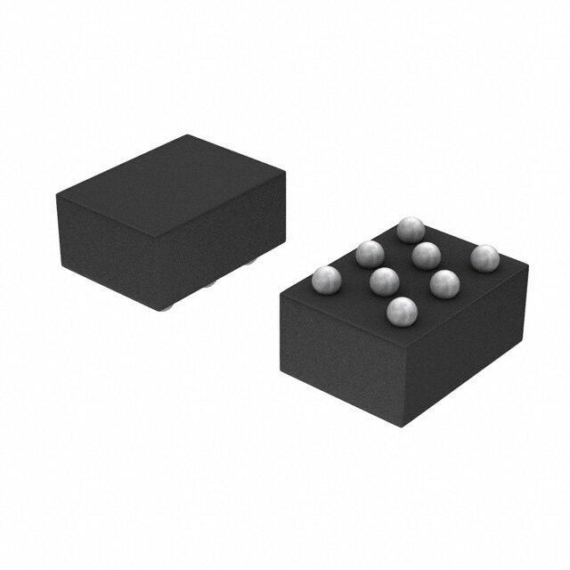
| 描述 | IC AMP AUDIO 1.5W MONO D 8TDFN |
| 产品分类 | |
| 品牌 | Intersil |
| 数据手册 | |
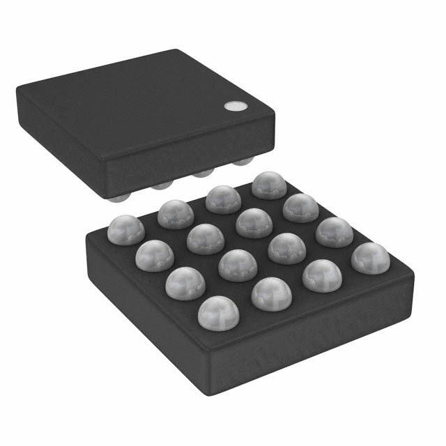
| 产品图片 |
|
| 产品型号 | ISL99201IRTCZ-TK |
| PCN设计/规格 | |
| rohs | 无铅 / 符合限制有害物质指令(RoHS)规范要求 |
| 产品系列 | - |
| 不同负载时的最大输出功率x通道数 | 1.4W x 1 @ 8 欧姆 |
| 供应商器件封装 | 8-TDFN(3x3) |
| 其它名称 | ISL99201IRTCZ-TKDKR |
| 包装 | Digi-Reel® |
| 安装类型 | 表面贴装 |
| 封装/外壳 | 8-WDFN 裸露焊盘 |
| 工作温度 | -40°C ~ 85°C (TA) |
| 标准包装 | 1 |
| 特性 | 消除爆音,差分输入,短路和热保护,关闭 |
| 电压-电源 | 2.4 V ~ 5.5 V |
| 类型 | D 类 |
| 输出类型 | 1-通道(单声道) |


- 商务部:美国ITC正式对集成电路等产品启动337调查
- 曝三星4nm工艺存在良率问题 高通将骁龙8 Gen1或转产台积电
- 太阳诱电将投资9.5亿元在常州建新厂生产MLCC 预计2023年完工
- 英特尔发布欧洲新工厂建设计划 深化IDM 2.0 战略
- 台积电先进制程称霸业界 有大客户加持明年业绩稳了
- 达到5530亿美元!SIA预计今年全球半导体销售额将创下新高
- 英特尔拟将自动驾驶子公司Mobileye上市 估值或超500亿美元
- 三星加码芯片和SET,合并消费电子和移动部门,撤换高东真等 CEO
- 三星电子宣布重大人事变动 还合并消费电子和移动部门
- 海关总署:前11个月进口集成电路产品价值2.52万亿元 增长14.8%


PDF Datasheet 数据手册内容提取
NOT RECOMMENDED FOR NEW DESIGNS DATASHEET NO RECOMMENDED REPLACEMENT contact our Technical Support Center at 1-888-INTERSIL or www.intersil.com/tsc ISL99201 FN6742 Filterless High Efficiency 1.5W Class D Mono Amplifier Rev 2.00 November 1, 2013 The ISL99201 is a fully integrated high efficiency class-D Features mono amplifier. It is designed to maximize performance for • Filterless class D with efficiency > 86% at 400mW mobile phone applications. The application circuit requires a minimum requirement of external components and operates • Click-pop suppression from a 2.4V to 5.5V input supply. It is capable of delivering • Slew rate control 1.4W of continuous output power with less than 1% THD+N driving a 8Ω load from a 5V supply. • Spread spectrum switching The ISL99201 features a high-efficiency, low-noise • Optional SYNC pin for master/slave operation without modulation scheme. It operates with 86% efficiency at interface 400mW into 8Ω and has a signal-to-noise ratio (SNR) that is • 1.4W into 8Ω with less than 1% THD+N better than 95dB. The ISL99201 has a micro-power • 2.4V to 5.5V single supply voltage shutdown mode with a typical shutdown current of 200nA. Shutdown is enabled by applying a logic low to the SD pin. • Built-in resistors to reduce board component count The architecture of the devices allows it to achieve very low • Only one external component required (Fixed gain mode) level of pop-and-click. This minimizes voltage glitches at the • Short circuit and thermal protection output during turn-on and turn-off, thus reducing audible noise on activation and deactivation. • Gain programmable 6dB, 9.6dB, 12dB and User programmable The fully differential input of the ISL99201 provides excellent rejection of common mode noise on the input typically 75dB. • Pb-Free (RoHS compliant) EMI suppression is achieved by SRC (Slew Rate Control). Applications The ISL99201 oscillator can be synchronized to an external clock through the SYNC input, allowing the switching • Mobile phones frequency to be externally defined. The SYNC input also • MP3 players allows multiple ISL99201 to be cascaded and frequency locked; minimizing interference due to clock intermodulation. • Portable gaming The ISL99201 also has excellent rejection of power supply • Portable electronics noise, including noise caused by GSM transmission bursts • Educational toys and RF rectification. PSRR is typically 75dB at 217Hz. There will be 4 versions of the part; they will consist of three fixed gain settings (6dB, 9. 6dB, 12dB) and one user programmable gain setting (need external resistors). The ISL99201 has built-in thermal shutdown and output short-circuit protection. FN6742 Rev 2.00 Page 1 of 11 November 1, 2013
ISL99201 Ordering Information PACKAGE PART PART GAIN SETTING TEMP. RANGE Tape and Reel PKG. NUMBER MARKING (dB) (°C) (Pb-Free) DWG. # ISL99201IRTAZ-T (Notes 1, 2) 201A 6 -40 to +85 8 Ld 3x3 TDFN L8.3x3A ISL99201IRTAZ-TK (Notes 1, 2) 201A 6 -40 to +85 8 Ld 3x3 TDFN L8.3x3A ISL99201IRTBZ-T (Notes 1, 2) 201B 9.6 -40 to +85 8 Ld 3x3 TDFN L8.3x3A ISL99201IRTBZ-TK (Notes 1, 2) 201B 9.6 -40 to +85 8 Ld 3x3 TDFN L8.3x3A ISL99201IRTCZ-T (Notes 1, 2) 201C 12 -40 to +85 8 Ld 3x3 TDFN L8.3x3A ISL99201IRTCZ-TK (Notes 1, 2) 201C 12 -40 to +85 8 Ld 3x3 TDFN L8.3x3A ISL99201IRTDZ-T (Notes 1, 2) 201D Prog. -40 to +85 8 Ld 3x3 TDFN L8.3x3A ISL99201IRTDZ-TK (Notes 1, 2) 201D Prog. -40 to +85 8 Ld 3x3 TDFN L8.3x3A ISL99201IRTAEVZ Evaluation Board ISL99201IRTBEVZ Evaluation Board ISL99201IRTCEVZ Evaluation Board ISL99201IRTDEVZ Evaluation Board NOTES: 1. Please refer to TB347or details on reel specifications. 2. These Intersil Pb-free plastic packaged products employ special Pb-free material sets, molding compounds/die attach materials, and 100% matte tin plate plus anneal (e3 termination finish, which is RoHS compliant and compatible with both SnPb and Pb-free soldering operations). Intersil Pb-free products are MSL classified at Pb-free peak reflow temperatures that meet or exceed the Pb-free requirements of IPC/JEDEC J STD-20. Pinout ISL99201 (8 LD TDFN) TOP VIEW SD 1 8 VO- SYNC 2 7 GND * IN+ 3 6 VDD IN- 4 5 VO+ FN6742 Rev 2.00 Page 2 of 11 November 1, 2013
ISL99201 Absolute Maximum Ratings (Reference to GND) Thermal Information Supply Voltage . . . . . . . . . . . . . . . . . . . . . . . . . . . . -0.3V to 6V Thermal Resistance (Typical Note 3) JA (°C/W) Input Voltage. . . . . . . . . . . . . . . . . . . . . . . . . . . . -0.3V to VDD+0.3V TDFN Package . . . . . . . . . . . . . . . . . . . . . . . . . . . 53 Maximum Junction Temperature (Plastic Package) -65°C to +150°C Recommended Operating Conditions Maximum Storage Temperature Range . . . . . . . . . -65°C to +150°C Power Dissipation Ratings Ambient Temperature Range . . . . . . . . . . . . . . . . . . -40°C to +85°C 8 Ld 3x3 TDFN Operating Supply Voltage (VDD Pin) . . . . . . . . . . . . . . 2.4V to 5.5V Derating Factor . . . . . . . . . . . . . . . . . . . . . . . . . . . . 21.8mW/°C Power Ratings TA = +25°C. . . . . . . . . . . . . . . . . . . . . . . . . . . . . . . . . . . 2.7W TA = +70°C . . . . . . . . . . . . . . . . . . . . . . . . . . . . . . . . . . 1.7W TA = +85°C. . . . . . . . . . . . . . . . . . . . . . . . . . . . . . . . . . . 1.4W Pb-Free Reflow Profile . . . . . . . . . . . . . . . . . . . . . . . . see link below http://www.intersil.com/pbfree/Pb-FreeReflow.asp CAUTION: Do not operate at or near the maximum ratings listed for extended periods of time. Exposure to such conditions may adversely impact product reliability and result in failures not covered by warranty. NOTE: 3. JA is measured in free air with the component mounted on a high effective thermal conductivity test board with “direct attach” features. See Tech Brief TB379 Electrical Specifications Typical Values Are Tested at VDD = 5V and the Ambient Temperature at +25°C. MIN MAX PARAMETER SYMBOL TEST CONDITIONS (Note 5) TYP (Note 5) UNITS Output Power Po RL = 8,THD = 10%, f = 1kHz, 20kHz BW, VDD = 5.0V 1.4 W RL = 8,THD = 10%, f = 1kHz, 20kHz BW, VDD = 3.6V 0.75 W RL = 8,THD = 10%, f = 1kHz, 20kHz BW, VDD = 2.5V 0.4 W RL = 8,THD = 1%, f = 1kHz, 20kHz BW, VDD = 5.0V 1.15 W Efficiency POUT = 1.4W, 833µH, VDD = 5.0V 90 % Total Harmonic Distortion + Ratio THD+N PO = 1W into 8 each channel, f = 1kHz, VDD = 5.0V 0.05 % PO = 0.5W into 8 each channel, f = 1kHz, VDD = 3.6V 0.05 % PO = 0.2W into 8 each channel, f = 1kHz, VDD = 3.6V 0.09 % Common-Mode Rejection Ratio CMRR VIC = 0.5V to (VDD - 0.8V); RL= 8VDD = 2.5V to 5.5V -60 dB CMRRGSM VCM = 2.5V ± 1VP-P at 217Hz, RL= 8 -60 dB Average Switching Frequency fsw VDD = 5V 300 375 450 kHz Differential Output Offset Voltage VOOS G = 6dB; 9.6dB; 12dB; 28dB. 0.2 5.0 mV POWER SUPPLY Supply Voltage Range VDD 2.4 5.5 V Power Supply Rejection Ratio PSRR VDD = 2.5V to 5.0V -65 dB PSRRGSM VRIPPLT = 100mVRMS at 217Hz (Input AC-Coupled with -65 dB 2µF capacitor) Supply Current IIN VIN = 0V, No load, VDD = 5V 3.9 mA VIN = 0V, No load, VDD = 3.6V 3.2 3.75 mA VIN = 0V, 833µH, VDD = 5V 3.9 mA VIN = 0V, 833µH, VDD = 3.6V 3.8 mA ISD SD = GND 0.2 0.4 µA (Note 4) FN6742 Rev 2.00 Page 3 of 11 November 1, 2013
ISL99201 Electrical Specifications Typical Values Are Tested at VDD = 5V and the Ambient Temperature at +25°C. (Continued) MIN MAX PARAMETER SYMBOL TEST CONDITIONS (Note 5) TYP (Note 5) UNITS GAIN CONTROL Closed-Loop Gain D version user program 27.5 28.5 29.5 dB (Max Gain, Ri = 0) A version 5.7 6 6.3 dB B version 9.2 9.6 10 dB C version 11.5 12 12.5 dB Differential Input Impedance ZIN SD = VDD, A version 70 k SD = VDD, B version 46.25 k SD = VDD, C version 35 k SD = VDD, D version, Ri = 2.5k 7.5 k SD = GND 100 k SHUTDOWN CONTROL Input Voltage High VIH 1.2 V Input Voltage Low VIL 0.5 V Turn-on Time tWU SD rising edge from GND to VDD 3.5 ms Turn-off Time tSD SD falling edge from VDD to GND 5 µs Output Impedance Z SD = GND >100 k OUT NOISE PERFORMANCE Output Voltage Noise En VDD = 3.6V, f = 20Hz to 20kHz, inputs are AC grounded, 27 µV AV= 6dB, A-weighting VDD = 3.6V, f = 20Hz to 20kHz, inputs are AC grounded, 35 µV AV0 = 6dB, no weighting Signal-to-Noise Ratio SNR POUT = 1W, RL = 8 102 dB NOTES: 4. Limits established by Characterization and are not production tested 5. Parameters with MIN and/or MAX limits are 100% tested at +25°C, unless otherwise specified. Temperature limits established by characterization and are not production tested. FN6742 Rev 2.00 Page 4 of 11 November 1, 2013
ISL99201 Pin Descriptions IN- SD Negative Differential Input. Shutdown Active Low. This signal is used to shut down and activate VO+ the part. It is 1.8V to 5V compatible. During shutdown, the part Positive BTL output. draws less than 100nA input current. Coming out of shutdown takes 3.5ms and going into shutdown is instantaneous. GND SYNC Ground. External clock input. This pin allows the chip to be synchronized to a VDD system clock. This helps in folding the spectral components and the Power Supply. switching harmonic out of band of interest. The range of SYNC frequency is from 250kHz to 800kHz. VO- IN+ Negative BTL output. Positive Differential Input. Block Diagram (Notes) SHUTDOWN CLICK AND POP SD LOGIC SUPPRESSION VDD SYNC1 GSEANWETROAOTTOHR +180° VDD + GATE DRIVE COMP WITH BIAS AND SRC VO- - REFERENCE OVER - CURRENT IN+ + - + COMP PROTECTION VDD + IN- - + - GATE DRIVE WITH VO+ SRC GND Notes: Gain = 6dB, 9.6dB, 12dB (gain setting) 140k Gain = ; with external resistor (Ri + 5kΩ) FN6742 Rev 2.00 Page 5 of 11 November 1, 2013
ISL99201 Typical Performance Characteristics 100 400 90 VDD = 2.5 V 350 80 A) 300 m Y (%) 6700 VDD = 3.6 V ENT ( 250 C R VDD = 2.5 V N 50 R 200 E U FFICI 40 VDD= 5 V LY C 150 VDD = 3.6 V E 30 P UP 100 20 S 10 RL= 8+ 33µH 50 VDD = 5 V RL= 8+ 33µH 0 0 0 0.25 0.50 0.75 1.00 1.25 1.50 1.75 0 0.25 0.50 0.75 1.0 1.25 1.50 1.75 OUTPUT POWER (W) OUTPUT POWER (W) FIGURE 1. EFFICIENCY vs OUTPUT POWER FIGURE 2. SUPPLY CURRENT vs OUTPUT POWER 5.0 100 %) RL= 8 RENT (mA) 44..05 RL= 8+ 33µH DISTORTION ( 10 VVVDDDDDD === 533V.V6V Y CUR 3.5 RL= NO LOAD MONIC 1 VDD = 2.5V PL 3.0 R UP HA0.10 S 2.5 AL T O T 2.0 0.01 2.5 3.0 3.5 4.0 4.5 5.0 5.5 6.0 0.01 0.10 1 10 INPUT SUPPLY (V) OUTPUT POWER (W) FIGURE 3. SUPPLY CURRENT vs SUPPLY VOLTAGE FIGURE 4. TOTAL HARMONIC DISTORTION + NOISE vs OUTPUT POWER -20 0.30 -30 VDD= 3.6V VIC = 1VP-P 0.25 MRR (COMMON MODEEJECTION RATIO - dB)-----8765400000 RL = 8 OWER DISSIPATION (W) 000...112050 CR P 0.05 -90 -100 0 10 100 1k 10k 100k 0 0.1 0.2 0.3 0.4 0.5 0.6 0.7 0.8 0.9 FREQUENCY (Hz) OUTPUT POWER (W) FIGURE 5. COMMON MODE REJECTION MODE vs FIGURE 6. POWER DISSIPATION vs OUTPUT POWER FREQUENCY FN6742 Rev 2.00 Page 6 of 11 November 1, 2013
ISL99201 Typical Performance Characteristics (Continued) 0.6 2.5 VDD = 5V RL = 8 0.5 RL = 8 f = 1kHz W) 2.0 GAIN = 4V/V N ( W) TIO 0.4 ER ( 1.5 PA W DISSI 0.3 UT PO 1.0 THD = 10% R 0.2 P E T OW OU THD = 1% P 0.1 0.5 0 0 0 0.25 0.50 0.75 1.00 1.25 1.50 2.5 3.0 3.5 4.0 4.5 5.0 OUTPUT POWER (W) SUPP L Y VOLTAGE (V) FIGURE 7. POWER DISSIPATION vs OUTPUT POWER FIGURE 8. OUTPUT POWER vs SUPPLY VOLTAGE 10 10 VDD = 2.5V VRDLD = =8 3.6V RL = 8 %) ONICOISE (%) 1 0.015W MONICNOISE ( 1 0.125W MN R+ 0.25W R+ 0.075W AN TOTAL HASTORTION 0.10 0.2W TOTAL HDISTORTIO 0.1 0.5W DI 0.01 0.01 10 100 1k 10k 100k 10 100 1k 10k 100k FREQUENCY (Hz) FREQUENCY (Hz) FIGURE 9. TOTAL HARMONIC DISTORTION + NOISE vs FIGURE 10. TOTAL HARMONIC DISTORTION + NOISE vs FREQUENCY FREQUENCY 10 -30 VDD = 5V INPUTSAC-GROUNDED VDD = 5V RL = 8 RL = 8 TOTAL HARMONIC ORTION + NOISE (%) 0.101 1W00..52W5W0.125W SUPPLY RIPPLEJECTION RATIO (dB) ---654000 CISLL =99 22µ0F1AVDD = 2.5V VDD = 3.6V T E S R -70 DI 0.01 10 100 1k 10k 100k -8010 100 1k 10k 100k FREQUENCY (Hz) FREQUENCY (Hz) FIGURE 11. TOTAL HARMONIC DISTORTION + NOISE vs FIGURE 12. SUPPLY RIPPLE REJECTION RATIO vs FREQUENCY FREQUENCY - ISL99201A FN6742 Rev 2.00 Page 7 of 11 November 1, 2013
ISL99201 Typical Performance Characteristics (Continued) -30 -30 INPUTSAC-GROUNDED VDD = 5V INPUTSAC-GROUNDED VDD = 5V RL = 8 RL = 8 dB) -40 CISLL =99 22µ0F1B dB) -40 CISLL =99 22µ0F1C EO ( EO ( PLY RIPPLTION RATI --6500 PLY RIPPLTION RATI --6500 VDD = 2.5V VDD = 3.6V PC PC UE UE SJ SJ RE -70 VDD = 3.6V RE -70 VDD = 2.5V -80 -80 10 100 1k 10k 100k 10 100 1k 10k 100k FREQUENCY (Hz) FREQUENCY (Hz) FIGURE 13. SUPPLY RIPPLE REJECTION RATIO vs FIGURE 14. SUPPLY RIPPLE REJECTION RATIO vs FREQUENCY - ISL99201B FREQUENCY - ISL99201C -20 -20 INPUTSFLOATING INPUTSFLOATING RL = 8 RL = 8 dB) -30 CISLL =99 22µ0F1A VDD = 3.6V dB) -30 CISLL =99 22µ0F1B VDD = 5V EO ( 40 EO ( -40 PLY RIPPLTION RATI -50 VDD = 5V PLY RIPPLTION RATI -50 VDD = 3.6V PC -60 PC -60 UE UE SJ SJ E E R -70 VDD = 2.5V R -70 VDD = 2.5V -80 -80 10 100 1k 10k 100k 10 100 1k 10k 100k FREQUENCY (Hz) FREQUENCY (Hz) FIGURE 15. SUPPLY RIPPLE REJECTION RATIO vs FIGURE 16. SUPPLY RIPPLE REJECTION RATIO vs FREQUENCY - ISL99201A FREQUENCY - ISL99201B -20 10 INPUTSFLOATING f = 1kHz SUPPLY RIPPLE REJECTION RATIO (dB) -----7654300000 RCISLLL ==99 822µ0F1C VDD = 3V.DV6DVD D= =5 V2.5V TOTAL HARMONIC REJECTION RATIO (%) 0.11 PO = 2002m.5WV5V 3.6V -80 0.01 10 100 1k 10k 100k 0 0.5 1.0 1.5 2.0 2.5 3.0 3.5 4.0 4.5 5.0 FREQUENCY (Hz) COMMON MODE INPUT VOLTAGE (V) FIGURE 17. SUPPLY RIPPLE REJECTION RATIO vs FIGURE 18. TOTAL HARMONIC DISTORTION + NOISE vs FREQUENCY - ISL99201C COMMON MODE INPUT VOLTAGE FN6742 Rev 2.00 Page 8 of 11 November 1, 2013
ISL99201 Typical Performance Characteristics (Continued) B) 0 0 d O ( -10 -10 ATI B) N R -20 DEO (d -20 PLY INPUT REJECTIO ----65430000 VDD = 2.5V VVDDDD == 53V.6V COMMON MO REJECTION RATI -----7654300000 VDD = 2.5V VDD = 3.V6VDD = 5V P U S -70 -80 0.25 0.75 1.25 1.75 2.25 2.75 3.25 3.75 4.25 4.75 5.25 0.25 1.25 2.25 3.25 4.25 5.25 DC COMMON MODE VOLTAGE (V) COMMON INPUT VOLTAGE (V) FIGURE 19. SUPPLY RIPPLE REJECTION RATIO vs DC FIGURE 20. COMMON MODE REJECTION RATIO vs COMMON COMMON MODE VOLTAGE MODE INPUT VOLTAGE Typical Applications VDD SAWTOOTH DIFFERENTIAL SYNC GENERATOR C3 INPUT ZIN RI VIN+ H-BRIDGE VO+ + POWER STAGE RI PWM AND - SR RI, REV D VIN- CONTROL VO- ZIN BIAS SD AND GND REFERENCE FIGURE 21. TYPICAL CIRCUIT WITH DIFFERENTIAL INPUT VDD SAWTOOTH SYNC GENERATOR C3 DIFFERENTIAL INPUT ZIN RI VIN+ H-BRIDGE VO+ + POWER STAGE RI PWM AND - SR VIN- CONTROL VO- ZIN RI, REV D BIAS SD AND GND REFERENCE FIGURE 22. TYPICAL CIRCUIT WITH DIFFERENTIAL INPUT AND INPUT CAPACITORS FN6742 Rev 2.00 Page 9 of 11 November 1, 2013
ISL99201 Typical Applications (Continued) VDD SAWTOOTH SYNC GENERATOR C3 DIFFERENTIAL INPUT ZIN C1 RI VIN+ H-BRIDGE VO+ POWER + STAGE C2 RI PWM AND - SR VIN- CONTROL VO- RI, REV D C1 = C2 = 1µF BIAS SD AND GND REFERENCE FIGURE 23. TYPICAL CIRCUIT WITH SINGLE-ENDED INPUT © Copyright Intersil Americas LLC 2009-2013. All Rights Reserved. All trademarks and registered trademarks are the property of their respective owners. For additional products, see www.intersil.com/en/products.html Intersil products are manufactured, assembled and tested utilizing ISO9001 quality systems as noted in the quality certifications found at www.intersil.com/en/support/qualandreliability.html Intersil products are sold by description only. Intersil may modify the circuit design and/or specifications of products at any time without notice, provided that such modification does not, in Intersil's sole judgment, affect the form, fit or function of the product. Accordingly, the reader is cautioned to verify that datasheets are current before placing orders. Information furnished by Intersil is believed to be accurate and reliable. However, no responsibility is assumed by Intersil or its subsidiaries for its use; nor for any infringements of patents or other rights of third parties which may result from its use. No license is granted by implication or otherwise under any patent or patent rights of Intersil or its subsidiaries. For information regarding Intersil Corporation and its products, see www.intersil.com FN6742 Rev 2.00 Page 10 of 11 November 1, 2013
ISL99201 Package Outline Drawing For the most recent package outline drawing, see L8.3x3A. L8.3x3A 8 LEAD THIN DUAL FLAT NO-LEAD PLASTIC PACKAGE Rev 4, 2/10 ( 2.30) 3.00 A ( 1.95) B ( 8X 0.50) 6 00 (1.50) 3. PIN 1 ( 2.90 ) INDEX AREA (4X) 0.15 PIN 1 TOP VIEW (6x 0.65) ( 8 X 0.30) TYPICAL RECOMMENDED LAND PATTERN SEE DETAIL "X" 2X 1.950 6X 0.65 0.75 ±0.05 0.10C C PIN #1 1 0.08C INDEX AREA SIDE VIEW 6 1.50 ±0.10 8 C 0 . 2 REF 5 8X 0.30 ±0.05 4 8X 0.30 ± 0.10 0.10M C AB 2.30 ±0.10 0 . 02 NOM. 0 . 05 MAX. BOTTOM VIEW DETAIL "X" NOTES: 1. Dimensions are in millimeters. Dimensions in ( ) for Reference Only. 2. Dimensioning and tolerancing conform to ASME Y14.5m-1994. 3. Unless otherwise specified, tolerance : Decimal ± 0.05 4. Dimension applies to the metallized terminal and is measured between 0.15mm and 0.20mm from the terminal tip. 5. Tiebar shown (if present) is a non-functional feature. 6. The configuration of the pin #1 identifier is optional, but must be located within the zone indicated. The pin #1 identifier may be either a mold or mark feature. 7. Compliant to JEDEC MO-229 WEEC-2 except for the foot length. FN6742 Rev 2.00 Page 11 of 11 November 1, 2013