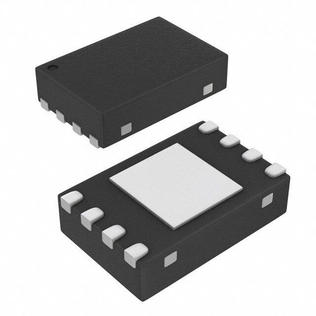
ICGOO在线商城 > ISL9103AIRUBZ-T
- 型号: ISL9103AIRUBZ-T
- 制造商: Intersil
- 库位|库存: xxxx|xxxx
- 要求:
| 数量阶梯 | 香港交货 | 国内含税 |
| +xxxx | $xxxx | ¥xxxx |
查看当月历史价格
查看今年历史价格
ISL9103AIRUBZ-T产品简介:
ICGOO电子元器件商城为您提供ISL9103AIRUBZ-T由Intersil设计生产,在icgoo商城现货销售,并且可以通过原厂、代理商等渠道进行代购。 提供ISL9103AIRUBZ-T价格参考¥7.10-¥14.32以及IntersilISL9103AIRUBZ-T封装/规格参数等产品信息。 你可以下载ISL9103AIRUBZ-T参考资料、Datasheet数据手册功能说明书, 资料中有ISL9103AIRUBZ-T详细功能的应用电路图电压和使用方法及教程。
| 参数 | 数值 |
| 产品目录 | 集成电路 (IC) |
| 描述 | IC REG BCK SYNC 1.5V 0.5A 6UTDFN |
| 产品分类 | |
| 品牌 | Intersil |
| 数据手册 | |
| 产品图片 |
|
| 产品型号 | ISL9103AIRUBZ-T |
| PWM类型 | 电流模式 |
| rohs | 无铅 / 符合限制有害物质指令(RoHS)规范要求 |
| 产品系列 | - |
| 产品培训模块 | http://www.digikey.cn/PTM/IndividualPTM.page?site=cn&lang=zhs&ptm=25476 |
| 供应商器件封装 | 6-UTDFN(1.6x1.6) |
| 其它名称 | ISL9103AIRUBZ-TCT |
| 包装 | 剪切带 (CT) |
| 同步整流器 | 是 |
| 安装类型 | 表面贴装 |
| 封装/外壳 | 6-UFDFN |
| 工作温度 | -40°C ~ 85°C |
| 标准包装 | 1 |
| 电压-输入 | 2.7 V ~ 6 V |
| 电压-输出 | 1.5V |
| 电流-输出 | 500mA |
| 类型 | 降压(降压) |
| 输出数 | 1 |
| 输出类型 | 固定 |
| 频率-开关 | 2.4MHz |







- 商务部:美国ITC正式对集成电路等产品启动337调查
- 曝三星4nm工艺存在良率问题 高通将骁龙8 Gen1或转产台积电
- 太阳诱电将投资9.5亿元在常州建新厂生产MLCC 预计2023年完工
- 英特尔发布欧洲新工厂建设计划 深化IDM 2.0 战略
- 台积电先进制程称霸业界 有大客户加持明年业绩稳了
- 达到5530亿美元!SIA预计今年全球半导体销售额将创下新高
- 英特尔拟将自动驾驶子公司Mobileye上市 估值或超500亿美元
- 三星加码芯片和SET,合并消费电子和移动部门,撤换高东真等 CEO
- 三星电子宣布重大人事变动 还合并消费电子和移动部门
- 海关总署:前11个月进口集成电路产品价值2.52万亿元 增长14.8%

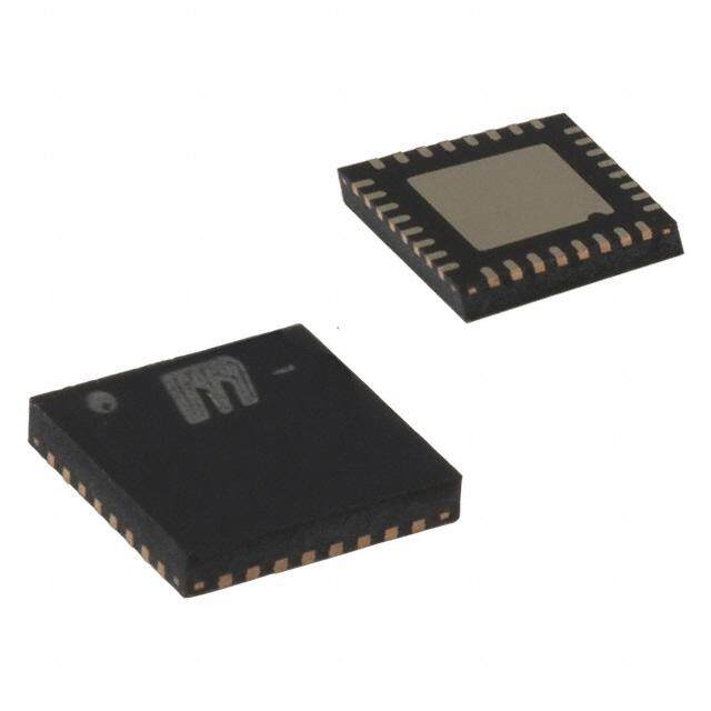

PDF Datasheet 数据手册内容提取
DATASHEET ISL9103, ISL9103A FN6828 500mA 2.4MHz Low IQ High Efficiency Synchronous Buck Converter Rev 3.00 December 9, 2015 The ISL9103, ISL9103A is a 500mA, 2.4MHz step-down Features regulator, which is ideal for powering low-voltage • High Efficiency Integrated Synchronous Buck Regulator microprocessors in compact devices such as PDAs and with up to 95% Efficiency cellular phones. It is optimized for generating low output voltages down to 0.8V. The supply voltage range is from • 2.7V to 6.0V Supply Voltage 2.7V to 6V allowing the use of a single Li+ cell, three NiMH • 2.4MHz PWM Switching Frequency cells or a regulated 5V input. It has guaranteed minimum output current of 500mA. A high switching frequency of • 500mA Guaranteed Output Current 2.4MHz pulse-width modulation (PWM) allows using small • 3% Output Accuracy Over-Temperature and Line for Fixed external components. Under light load condition, the device Output Options operates at low IQ skip mode with typical 20µA quiescent • 20µA Quiescent Supply Current in Skip Mode current for highest light load efficiency to maximize battery life, and it automatically switches to fixed frequency PWM • Less than 1µA Logic Controlled Shutdown Current mode under heavy load condition. • 100% Maximum Duty Cycle for Lowest Dropout The ISL9103, ISL9103A includes a pair of low • Ultrasonic Switching Frequency at Skip Mode to Prevent ON-resistance P-Channel and N-Channel internal MOSFETs Audible Frequency Noise (For ISL9103A Only) to maximize system efficiency and minimize the external • Discharge Output Capacitor when Disabled component count. 100% duty-cycle operation allows less than 300mV dropout voltage at 500mA. • Internal Digital Soft-Start The ISL9103, ISL9103A offers internal digital soft-start, • Peak Current Limiting, Short Circuit Protection enable for power sequence, overcurrent protection and • Over-Temperature Protection thermal shutdown functions. In addition, the ISL9103, ISL9103A offers a quick bleeding function that discharges • Chip Enable the output capacitor when the IC is disabled. • Small 6 Pin 1.6mmx1.6mm UTDFN Package The ISL9103, ISL9103A is offered in a 1.6x1.6mm UTDFN • Pb-Free (RoHS Compliant) package. The complete converter occupies less than 0.5cm2. Applications • Single Li-ion Battery-Powered Equipment Pinout • Mobile Phones and MP3 Players ISL9103, ISL9103A (6 LD 1.6x1.6 UTDFN) • PDAs and Palmtops TOP VIEW • WCDMA Handsets VIN 1 6 SW • Portable Instruments EN 2 5 GND NC 3 4 FB FN6828 Rev 3.00 Page 1 of 14 December 9, 2015
ISL9103, ISL9103A Pin Descriptions PIN NUMBER PIN NAME DESCRIPTION 1 VIN Input supply voltage. Typically connect a 10µF ceramic capacitor to ground. 2 EN Regulator enable pin. Enable the device when driven to high. Shut down the chip and discharge output capacitor when driven to low. Do not leave this pin floating. 3 NC No connect; leave floating. 4 FB Buck converter output feedback pin. For adjustable output version, its typical value is 0.8V and connect it to the output through a resistor divider for desired output voltage; for fixed output version, directly connect this pin to the converter output. 5 GND Ground connection. 6 SW Switching node connection. Connect to one terminal of inductor. Ordering Information OUTPUT TEMP PACKAGE PART NUMBER PART VOLTAGE (V) RANGE Tape and Reel PKG ULTRASONIC (Notes 1, 3, 4) MARKING (Note 2) (°C) (RoHS Compliant) DWG. # FUNCTION ISL9103IRUJZ-T J1 2.8 -40 to +85 6 Ld UTDFN L6.1.6x1.6 NO (No longer available, recommended replacement:ISL9103AIRUJZ-T) ISL9103IRUFZ-T J2 2.5 -40 to +85 6 Ld UTDFN L6.1.6x1.6 NO (No longer available, recommended replacement: ISL9103AIRUFZ-T) ISL9103IRUDZ-T J3 2.0 -40 to +85 6 Ld UTDFN L6.1.6x1.6 NO (No longer available, recommended replacement: ISL9103AIRUDZ-T) ISL9103IRUCZ-T J4 1.8 -40 to +85 6 Ld UTDFN L6.1.6x1.6 NO (No longer available, recommended replacement: ISL9103AIRUCZ-T) ISL9103IRUBZ-T J5 1.5 -40 to +85 6 Ld UTDFN L6.1.6x1.6 NO (No longer available, recommended replacement: ISL9103AIRUBZ-T) ISL9103IRUWZ-T J6 1.2 -40 to +85 6 Ld UTDFN L6.1.6x1.6 NO (No longer available, recommended replacement: ISL9103AIRUWZ-T) ISL9103IRUAZ-T J7 ADJ -40 to +85 6 Ld UTDFN L6.1.6x1.6 NO (No longer available, recommended replacement: ISL9103AIRUAZ-T) ISL9103AIRUJZ-T J9 2.8 -40 to +85 6 Ld UTDFN L6.1.6x1.6 YES ISL9103AIRUFZ-T K0 2.5 -40 to +85 6 Ld UTDFN L6.1.6x1.6 YES ISL9103AIRUDZ-T K1 2.0 -40 to +85 6 Ld UTDFN L6.1.6x1.6 YES ISL9103AIRUCZ-T K2 1.8 -40 to +85 6 Ld UTDFN L6.1.6x1.6 YES ISL9103AIRUBZ-T K3 1.5 -40 to +85 6 Ld UTDFN L6.1.6x1.6 YES ISL9103AIRUWZ-T K4 1.2 -40 to +85 6 Ld UTDFN L6.1.6x1.6 YES ISL9103AIRUAZ-T K5 ADJ -40 to +85 6 Ld UTDFN L6.1.6x1.6 YES NOTES: 1. Please refer to TB347 for details on reel specifications. 2. Other output voltage options may be available upon request, please contact Intersil for more details. 3. These Intersil Pb-free plastic packaged products employ special Pb-free material sets; molding compounds/die attach materials and NiPdAu plate - e4 termination finish, which is RoHS compliant and compatible with both SnPb and Pb-free soldering operations. Intersil Pb-free products are MSL classified at Pb-free peak reflow temperatures that meet or exceed the Pb-free requirements of IPC/JEDEC J STD-020. 4. For Moisture Sensitivity Level (MSL), please see device information page for ISL9103, ISL9103A. For more information on MSL please see techbrief TB363. FN6828 Rev 3.00 Page 2 of 14 December 9, 2015
ISL9103, ISL9103A Absolute Maximum Ratings Thermal Information VIN, EN to GND. . . . . . . . . . . . . . . . . . . . . . . . . . . . . . -0.3V to 6.5V Thermal Resistance (Typical, Note 5) JA (°C/W) SW to GND . . . . . . . . . . . . . . . . . . . . . . . . . . . . . . . . . -1.5V to 6.5V 6 Ld 1.6x1.6 UTDFN Package. . . . . . . . . . . . . . . . . 160 FB to GND (for adjustable version) . . . . . . . . . . . . . . . -0.3V to 2.7V Junction Temperature Range. . . . . . . . . . . . . . . . . .-40°C to +125°C FB to GND (for fixed output version) . . . . . . . . . . . . . . -0.3V to 3.6V Storage Temperature Range . . . . . . . . . . . . . . . . . .-65°C to +150°C Recommended Operating Conditions Pb-free Reflow Profile . . . . . . . . . . . . . . . . . . . . . . . . .see link below http://www.intersil.com/pbfree/Pb-FreeReflow.asp VIN Supply Voltage Range . . . . . . . . . . . . . . . . . . . . . .2.7V to 6.0V Load Current . . . . . . . . . . . . . . . . . . . . . . . . . . . . . . . . .up to 500mA Ambient Temperature Range. . . . . . . . . . . . . . . . . . .-40°C to +85°C CAUTION: Do not operate at or near the maximum ratings listed for extended periods of time. Exposure to such conditions may adversely impact product reliability and result in failures not covered by warranty. NOTE: 5. JA is measured with the component mounted on a high effective thermal conductivity test board in free air. See Tech Brief TB379 for details. Electrical Specifications Unless otherwise noted, all parameter limits are guaranteed over the recommended operating conditions and the typical specifications are measured at the following conditions: TA = +25°C, VIN = VEN = 3.6V, L = 2.2µH, C1 = 10µF, C2 = 10µF, IOUT = 0A (see “Typical Applications” on page8). Boldface limits apply over the operating temperature range, -40°C to +85°C. MIN MAX PARAMETER SYMBOL TEST CONDITIONS (Note6) TYP (Note 6) UNITS SUPPLY Undervoltage Lockout Threshold (UVLO) VUVLO TA = +25°C, Rising - 2.5 2.7 V UVLO Hysteresis 50 150 - mV Quiescent Supply Current (for ISL9103 IVIN1 In skip mode, no load at the output, no switch, - 20 34 µA Adjustable Output Voltage Only) VIN = 6.0V Quiescent Supply Current (for ISL9103A IVIN2 In skip mode, no load at the output, no switch, - 32 45 µA Adjustable Output Only) VIN = 6.0V Shut Down Supply Current ISD VIN = 6.0V, EN = LOW - 0.05 1 A OUTPUT REGULATION FB Voltage Accuracy (for Adjustable Output TA = 0°C to +85°C -2 - +2 % Only) -2.5 - +2.5 % FB Voltage VFB 0.8 V FB Bias Current (for Adjustable Output Only) IFB VFB = 0.75V - 5 100 nA Output Voltage Accuracy (for Fixed Output -3 - 3 % PWM Mode Voltage Only) Line Regulation VIN = VO + 0.5V to 6V (minimal 2.7V) - 0.2 - %/V Load Regulation VIN = 3.6V, IO = 150mA to 500mA - 0.0009 - %/mA SW P-Channel MOSFET ON-Resistance VIN = 3.6V, IO = 200mA - 0.45 0.6 VIN = 2.7V, IO = 200mA - 0.55 0.72 N-Channel MOSFET ON-Resistance VIN = 3.6V, IO = 200mA - 0.4 0.52 VIN = 2.7V, IO = 200mA - 0.5 0.65 N-Channel Bleeding MOSFET - 100 - ON-Resistance P-Channel MOSFET Peak Current Limit IPK VIN = 4.2V 0.7 0.95 1.30 A Maximum Duty Cycle - 100 - % SW Leakage Current SW at Hi-Z state - 0.01 2 µA PWM Switching Frequency fS VIN = 3.6V 1.9 2.4 2.75 MHz FN6828 Rev 3.00 Page 3 of 14 December 9, 2015
ISL9103, ISL9103A Electrical Specifications Unless otherwise noted, all parameter limits are guaranteed over the recommended operating conditions and the typical specifications are measured at the following conditions: TA = +25°C, VIN = VEN = 3.6V, L = 2.2µH, C1 = 10µF, C2 = 10µF, IOUT = 0A (see “Typical Applications” on page8). Boldface limits apply over the operating temperature range, -40°C to +85°C. (Continued) MIN MAX PARAMETER SYMBOL TEST CONDITIONS (Note6) TYP (Note 6) UNITS SW Minimum On-Time - 65 - ns Soft-Start-Up Time - 1.2 - ms EN Logic Input Low - - 0.4 V Logic Input High 1.4 - - V Logic Input Leakage Current - 0.1 1 µA Thermal Shutdown - 130 - °C Thermal Shutdown Hysteresis - 30 - °C NOTE: 6. Parameters with MIN and/or MAX limits are 100% tested at +25°C, unless otherwise specified. Temperature limits established by characterization and are not production tested Typical Operating Performance 100 100 VIN = 2.7V 90 90 80 80 Y (%) 6700 VIN = 3.8V VIN = 4.9V Y (%) 6700 VIN = 3.5V VIN = 4.5V VIN = 5.5V C C N 50 N 50 E E FICI 40 FICI 40 EF 30 EF 30 20 20 10 10 0 0 0 0.1 0.2 0.3 0.4 0.5 0 0.1 0.2 0.3 0.4 0.5 IO (A) IO (A) FIGURE 1. EFFICIENCY vs LOAD CURRENT (VO = 1.5V) FIGURE 2. EFFICIENCY vs LOAD CURRENT (VO = 2.5V) 30 1.800 T = +85°C 1.795 VIN = 3.6V, RISING 25 T = +25°C 1.790 A) V) q (µ 20 V (O I 1.785 VIN = 3.6V, FALLING 15 1.780 T = -45°C 10 1.775 2.70 3.25 3.80 4.35 4.90 5.45 6.00 0 100 200 300 400 500 VIN (V) IOUT (mA) FIGURE 3. INPUT QUIESCENT CURRENT vs VIN (VO = 2.5V) FIGURE 4. OUTPUT VOLTAGE vs LOAD CURRENT (ISL9103,VO_NORMINAL = 1.8V) FN6828 Rev 3.00 Page 4 of 14 December 9, 2015
ISL9103, ISL9103A Typical Operating Performance (Continued) 2.520 5V/DIV 2.515 VSW VIN = 4.0V, RISING 2.510 VOUT (V)O 1V/DIV V 2.505 VIN = 4.0V, FALLING 200mA/DIV 2.500 IL 2.495 5V/DIV EN 0 100 200 300 400 500 IOUT(mA) FIGURE 5. OUTPUT VOLTAGE vs LOAD CURRENT FIGURE 6. SOFT-START TO PFM MODE (VIN = 3.6V, (ISL9103,VO_NORMINAL = 2.5V) VOUT=1.5V, IOUT = 0.001mA) 5V/DIV 5V/DIV VSW VSW VOUT VOUT 1V/DIV 2V/DIV 500mA/DIV IL 200mA/DIV IL 5V/DIV EN 5V/DIV EN FIGURE 7. SOFT-START TO PWM MODE (VIN = 3.6V, FIGURE 8. SOFT-START TO PFM MODE (VIN = 3.6V, VOUT=1.5V, IOUT = 500mA) VOUT=2.5V, IOUT = 0.001mA) 5V/DIV 5V/DIV VSW VSW 50mV/DIV 50mV/DIV VOUT VOUT Io 20mA/DIV 20mA/DIV Io FIGURE 9. LOAD TRANSIENT IN PFM MODE (VIN = 3.6V, FIGURE 10. LOAD TRANSIENT IN PFM MODE (VIN = 3.6V, VOUT = 1.5V, 5mA TO 30mA) VOUT = 1.5V, 30mA TO 5mA) FN6828 Rev 3.00 Page 5 of 14 December 9, 2015
ISL9103, ISL9103A Typical Operating Performance (Continued) 5V/DIV 5V/DIV VSW VSW 50mV/DIV VOUT 50mV/DIV VOUT 20mA/DIV IL 20mA/DIV IL FIGURE 11. LOAD TRANSIENT IN PFM MODE (VIN = 3.6V, FIGURE 12. LOAD TRANSIENT IN PFM MODE (VIN = 3.6V, VOUT = 2.5V, 5mA TO 30mA) VOUT = 2.5V, 30mA TO 5mA) 5V/DIV 5V/DIV VSW VSW 50mV/DIV 50mV/DIV VOUT VOUT Io Io 200mA/DIV 200mA/DIV FIGURE 13. LOAD TRANSIENT FROM PFM TO PWM MODE FIGURE 14. LOAD TRANSIENT FROM PWM TO PFM MODE (VIN = 3.6V, VOUT = 1.5V, 5mA TO 300mA) (VIN = 3.6V, VOUT = 1.5V, 300mA TO 5mA) 5V/DIV 5V/DIV VSW VSW 50mV/DIV 50mV/DIV VOUT (AC COUPLED) VOUT (AC COUPLED) 200mA/DIV 200mA/DIV IL IL FIGURE 15. LOAD TRANSIENT FROM PFM TO PWM MODE FIGURE 16. LOAD TRANSIENT FROM PWM TO PFM MODE (VIN = 3.6V, VOUT = 2.5V, 5mA TO 300mA) (VIN = 3.6V, VOUT = 2.5V, 300mA TO 5mA) FN6828 Rev 3.00 Page 6 of 14 December 9, 2015
ISL9103, ISL9103A Typical Operating Performance (Continued) 5V/DIV 5V/DIV VSW VSW 50mV/DIV 50mV/DIV VOUT VOUT (AC COUPLED) 500mA/DIV 500mA/DIV Io Io FIGURE 17. LOAD TRANSIENT IN PWM MODE (VIN = 3.6V, FIGURE 18. LOAD TRANSIENT IN PWM MODE (VIN = 3.6V, VO= 1.5V, 200mA TO 500mA) VO= 1.5V, 500mA TO 200mA) 5V/DIV 5V/DIV VSW VSW 50mV/DIV VOUT 50mV/DIV VOUT 500mA/DIV Io 500mA/DIV Io FIGURE 19. LOAD TRANSIENT IN PWM MODE (VIN = 3.6V, FIGURE 20. LOAD TRANSIENT IN PWM MODE (VIN = 3.6V, VO= 2.5V, 200mA TO 500mA) VO= 2.5V, 500mA TO 200mA) FN6828 Rev 3.00 Page 7 of 14 December 9, 2015
ISL9103, ISL9103A Typical Applications ISL9103, ISL9103A ADJUSTABLE OUTPUT L OUTPUT INPUT: 2.7V TO 6V 2.2µH UP TO 500mA VIN SW C2 C1 10µF R1 C3 10µF 100k 47pF R2 ENABLE 100k EN FB DISABLE GND ISL9103, ISL9103A FIXED OUTPUT L OUTPUT INPUT: 2.7V TO 6V 2.2µH UP TO 500mA VIN SW C2 C1 10µF 10µF ENABLE EN FB DISABLE GND FIGURE 21. TYPICAL APPLICATIONS DIAGRAM Note: For adjustable output version, the internal feedback resistor divider is disabled and the FB pin is directly connected to the error amplifier. TABLE 1. BILL OF MATERIALS PARTS DESCRIPTION MANUFACTURERS PART NUMBER SPECIFICATIONS SIZE L Inductor Sumida CDRH2D14NP-2R2NC 2.2µH 3.2mmx3.2mm Input and output C1, C2 Panasonic ECJ-1VB1A106M 10µF/10V, X5R 0603 capacitor C3 Capacitor KEMET C0402C470J5GACTU 47pF/50V 0402 R1, R2 Resistor Various - 100kSMD, 1% 0402 FN6828 Rev 3.00 Page 8 of 14 December 9, 2015
ISL9103, ISL9103A Block Diagram SO SHUTDOWN SHUTDOWN SSTSOFATTFRATT- RT OSCILLATOR VIN EN BANDGAP VREF + EAMP + PWM/PFM COMP LOGIC CONTROLLER PROTECTION SW DRIVER SLOPE COMP X GND *NOTE FB BLEEDING FET 100 + + CSA OCP VREF1 SCP VREF3 + + SKIP VREF2 ZERO-CROSS SENSING *NOTE: FOR FIXED OUTPUT OPTIONS ONLY NOTE: For Adjustable output version, the internal feedback resistor divider is disabled and the FB pin is directly connected to the error amplifier. FIGURE 22. FUNCTIONAL BLOCK DIAGRAM Theory of Operation The PWM operation is initialized by the clock from the oscillator. The P-Channel MOSFET is turned on at the The ISL9103, ISL9103A is a step-down switching regulator beginning of a PWM cycle and the current in the P-Channel optimized for battery-powered handheld applications. The MOSFET starts ramping up. When the sum of the CSA output regulator operates at typical 2.4MHz fixed switching frequency and the compensation slope reaches the control reference of under heavy load condition to allow small external inductor and the current loop, the PWM comparator COMP sends a signal capacitors to be used for minimal printed-circuit board (PCB) to the PWM logic to turn off the P-Channel MOSFET and to area. At light load, the regulator can automatically enter the turn on the N-Channel MOSFET. The N-MOSFET remains on till skip mode (PFM mode) to reduce the switching frequency to the end of the PWM cycle. Figure 23 shows the typical operating minimize the switching loss and to maximize the battery life. waveforms during the normal PWM operation. The dotted lines The quiescent current under skip mode, and under no load and illustrate the sum of the slope compensation ramp and the CSA no switch condition is typically only 20µA. The supply current is output. typically only 0.05µA when the regulator is disabled. PWM Control Scheme The ISL9103, ISL9103A uses the peak-current-mode pulse-width modulation (PWM) control scheme for fast transient response and pulse-by-pulse current limiting. Figure 22 shows the circuit functional block diagram. The current loop consists of the oscillator, the PWM comparator COMP, current sensing circuit, and the slope compensation for the current loop stability. The current sensing circuit consists of the resistance of the P-Channel MOSFET when it is turned on and the Current Sense Amplifier (CSA). The control reference for the current loops comes from the Error Amplifier (EAMP) of the voltage loop. FN6828 Rev 3.00 Page 9 of 14 December 9, 2015
ISL9103, ISL9103A During the 16-consecutive cycles, the inductor current could be negative. The counter is reset to zero when the sensed current v EAMP flowing through SW node does not cross zero during any cycle within the 16-consecutive cycles. Once ISL9103, ISL9103A v CSA enters the skip mode, the pulse modulation starts being controlled by the SKIP comparator shown in Figure 22. Each d pulse cycle is still synchronized by the PWM clock. The P-Channel MOSFET is turned on at the rising edge of clock i and turned off when its current reaches ~20% of the peak L current limit. As the average inductor current in each cycle is v higher than the average current of the load, the output voltage OUT rises cycle over cycle. When the output voltage is sensed to reach 1.5% above its nominal voltage, the P-Channel FIGURE 23. PWM OPERATION WAVEFORMS MOSFET is turned off immediately and the inductor current is fully discharged to zero and stays at zero. The output voltage The output voltage is regulated by controlling the reference reduces gradually due to the load current discharging the voltage to the current loop. The bandgap circuit outputs a 0.8V output capacitor. When the output voltage drops to the nominal reference voltage to the voltage control loop. The feedback voltage, the P-Channel MOSFET will be turned on again, signal comes from the FB pin. The soft-start block only affects repeating the previous operations. the operation during the start-up and will be discussed separately in “Soft-Start” on page11. The EAMP is a The regulator resumes normal PWM mode operation when the transconductance amplifier, which converts the voltage error output voltage is sensed to drop below 1.5% of its nominal signal to a current output. The voltage loop is internally voltage value. compensated by a RC network. The maximum EAMP voltage Enable output is precisely clamped to the bandgap voltage. The enable (EN) pin allows user to enable or disable the Skip Mode (PFM Mode) converter for purposes such as power-up sequencing. With EN Under light load condition, ISL9103, ISL9103A automatically pin pulled to high, the converter is enabled and the internal enters a pulse-skipping mode to minimize the switching loss by reference circuit wakes up first and then the soft start-up reducing the switching frequency. Figure 24 illustrates the skip begins. When EN pin is pulled to logic low, the converter is mode operation. A zero-cross sensing circuit (as shown in disabled, both P-Channel MOSFET and N-Channel MOSFETS Figure 22) monitors the current flowing through SW node for are turned off, and the output capacitor is discharged through zero crossing. When it is detected to cross zero for internal discharge path. 16-consecutive cycles, the regulator enters the skip mode. 16 CYCLES CLOCK 20% PEAK CURRENT LIMIT IL 0 1.015*VOUT_NOMINAL VOUT VOUT_NOMINAL FIGURE 24. SKIP MODE OPERATION WAVEFORMS FN6828 Rev 3.00 Page 10 of 14 December 9, 2015
ISL9103, ISL9103A Overcurrent Protection The overcurrent protection is provided on ISL9103, ISL9103A V 1–-V-----O--- when overload condition happens. It is realized by monitoring the O VIN I = --------------------------------------- CSA output with the OCP comparator, as shown in Figure22. LfS (EQ. 1) When the current at P-Channel MOSFET is sensed to reach the In Equation 1, usually the typical values can be used but to current limit, the OCP comparator is triggered to turn off the P- have a more conservative estimation, the inductance should Channel MOSFET immediately. consider the value with worst case tolerance; and for switching frequency fS, the minimum fS from the “Electrical Short-Circuit Protection Specifications” table on page3 can be used. ISL9103, ISL9103A has a Short-Circuit Protection (SCP) To select the inductor, its saturation current rating should be at comparator, which monitors the FB pin voltage for output short- least higher than the sum of the maximum output current and circuit protection. When the output voltage is sensed to be half of the delta calculated from Equation 1. Another more lower than a certain threshold, the SCP comparator reduces conservative approach is to select the inductor with the current the PWM oscillator frequency to a much lower frequency to rating higher than the P-Channel MOSFET peak current limit. protect the IC from being damaged. Another consideration is the inductor DC resistance since it Undervoltage Lockout (UVLO) directly affects the efficiency of the converter. Ideally, the When the input voltage is below the Undervoltage Lock Out inductor with the lower DC resistance should be considered to (UVLO) threshold, ISL9103, ISL9103A is disabled. achieve higher efficiency. Soft-Start Inductor specifications could be different from different manufacturers so please check with each manufacturer if The soft-start feature eliminates the inrush current during the additional information is needed. circuit start-up. The soft-start block outputs a ramp reference to both the voltage loop and the current loop. The two ramps limit For the output capacitor, a ceramic capacitor can be used the inductor current rising speed as well as the output voltage because of the low ESR values, which helps to minimize the speed so that the output voltage rises in a controlled fashion. output voltage ripple. A typical value of 10µF ceramic capacitor should be enough for most of the applications and the Low Dropout Operation capacitor should be X5R or X7R. The ISL9103, ISL9103A features low dropout operation to maximize the battery life. When the input voltage drops to a Input Capacitor Selection level that ISL9103, ISL9103A can no longer operate under The main function for the input capacitor is to provide switching regulation to maintain the output voltage, the decoupling of the parasitic inductance and to provide filtering P-Channel MOSFET is completely turned on (100% duty function to prevent the switching current from flowing back to cycle). The dropout voltage under such condition is the product the battery rail. A 10µF ceramic capacitor (X5R or X7R) is a of the load current and the ON-resistance of the P-Channel good starting point for the input capacitor selection. MOSFET. Minimum required input voltage VIN under this condition is the sum of output voltage plus the voltage drop Output Voltage Setting Resistor Selection cross the inductor and the P-Channel MOSFET switch. For ISL9103, ISL9103A adjustable output option, the voltage Thermal Shut Down resistors, R1 and R2, as shown in Figure 21, set the desired output voltage values. The output voltage can be calculated The ISL9103, ISL9103A provides built-in thermal protection using Equation 2: function. The thermal shutdown threshold temperature is +130°C (typ) with a 30°C (typ) hysteresis. When the internal R1 V = V 1+------- temperature is sensed to reach +130°C, the regulator is O FB R2 (EQ. 2) completely shut down and as the temperature drops to +100°C (typ), the ISL9103, ISL9103A resumes operation starting from where VFB is the feedback voltage (typically it is 0.8V). The the soft-start. current flowing through the voltage divider resistors can be Applications Information calculated as VO/(R1 + R2), so larger resistance is desirable to minimize this current. On the other hand, the FB pin has Inductor and Output Capacitor Selection leakage current that will cause error in the output voltage setting. The leakage current has a typical value of 0.1µA. To To achieve better steady state and transient response, minimize the accuracy impact on the output voltage, select the ISL9103, ISL9103A typically uses a 2.2µH inductor. The peak- to-peak inductor current ripple can be expressed in Equation 1: R2 no larger than 200k. FN6828 Rev 3.00 Page 11 of 14 December 9, 2015
ISL9103, ISL9103A For adjustable output versions, C3 (shown in Figure 21) is Layout Recommendation highly recommended for improving stability and achieving The PCB layout is a very important converter design step to better transient response. make sure the designed converter works well, especially under the high current high switching frequency condition. Table 2 provides the recommended component values for some output voltage options. For ISL9103, ISL9103A, the power loop is composed of the TABLE 2. RECOMMENDED ISL9103, ISL9103A ADJUSTABLE output inductor L, the output capacitor COUT, the SW pin and OUTPUT VERSION CIRCUIT CONFIGURATION vs the PGND pin. It is necessary to make the power loop as VOUT small as possible and the connecting traces among them VOUT L C2 R1 C3 R2 should be direct, short and wide; the same type of traces (V) (µH) µF) (k (pF) (k should be used to connect the VIN pin, the input capacitor 0.8 2.2 10 0 N/A N/A CIN and its ground. 1.0 2.2 10 44.2 100 178 The switching node of the converter, the SW pin, and the traces connected to this node are very noisy, so keep the 1.2 2.2 10 80.6 47 162 voltage feedback trace and other noise sensitive traces 1.5 2.2 10 84.5 47 97.6 away from these noisy traces. 1.8 2.2 10 100 47 80.6 The input capacitor should be placed as close as possible to 2.5 2.2 10 100 47 47.5 the VIN pin. The ground of the input and output capacitors should be connected as close as possible as well. In 2.8 2.2 10 100 47 40.2 addition, a solid ground plane is helpful for EMI performance. 3.3 2.2 10 102 47 32.4 © Copyright Intersil Americas LLC 2009-2015. All Rights Reserved. All trademarks and registered trademarks are the property of their respective owners. For additional products, see www.intersil.com/en/products.html Intersil products are manufactured, assembled and tested utilizing ISO9001 quality systems as noted in the quality certifications found at www.intersil.com/en/support/qualandreliability.html Intersil products are sold by description only. Intersil may modify the circuit design and/or specifications of products at any time without notice, provided that such modification does not, in Intersil's sole judgment, affect the form, fit or function of the product. Accordingly, the reader is cautioned to verify that datasheets are current before placing orders. Information furnished by Intersil is believed to be accurate and reliable. However, no responsibility is assumed by Intersil or its subsidiaries for its use; nor for any infringements of patents or other rights of third parties which may result from its use. No license is granted by implication or otherwise under any patent or patent rights of Intersil or its subsidiaries. For information regarding Intersil Corporation and its products, see www.intersil.com FN6828 Rev 3.00 Page 12 of 14 December 9, 2015
ISL9103, ISL9103A Revision History The revision history provided is for informational purposes only and is believed to be accurate, but not warranted. Please go to the web to make sure that you have the latest revision. DATE REVISION CHANGE December 9, 2015 FN6828.3 Updated the Ordering Information table on page2. Added Revision History and About Intersil sections. Updated Package Outline Drawing L6.1.6X1.6 to the latest revision. Changes are as follows: -Side View- changed thickness from 0.55 to 0.5 ±0.05. -Tiebar Note updated From: Tiebar shown (if present) is a non-functional feature. To: Tiebar shown (if present) is a non-functional feature and may be located on any of the 4 sides (or ends). About Intersil Intersil Corporation is a leading provider of innovative power management and precision analog solutions. The company's products address some of the largest markets within the industrial and infrastructure, mobile computing and high-end consumer markets. For the most updated datasheet, application notes, related documentation and related parts, please see the respective product information page found at www.intersil.com. You may report errors or suggestions for improving this datasheet by visiting www.intersil.com/ask. Reliability reports are also available from our website at www.intersil.com/support. FN6828 Rev 3.00 Page 13 of 14 December 9, 2015
ISL9103, ISL9103A Package Outline Drawing L6.1.6x1.6 6 LEAD ULTRA THIN DUAL FLAT NO-LEAD COL PLASTIC PACKAGE (UTDFN COL) Rev 3, 05/15 2X 1.00 1.60 A PIN #1 INDEX AREA 6 6 4X 0.50 PIN 1 INDEX AREA B 1 3 5X 0 . 40 ± 0 . 1 1X 0.5 ±0.1 1.60 (4X) 0.15 6 4 0.10M C AB TOP VIEW 4 0.25 +0.05 / -0.07 BOTTOM VIEW ( 6X 0 . 25 ) SEE DETAIL "X" ( 1X 0 .70 ) 0.5 ±0.05 0.10 C C BASE PLANE SEATING PLANE ( 1 . 4 ) 0.08 C SIDE VIEW 5 0 . 2 REF C ( 5X 0 . 60 ) 0 . 00 MIN. 0 . 05 MAX. ( 4X 0 . 5 ) DETAIL "X" TYPICAL RECOMMENDED LAND PATTERN NOTES: 1. Dimensions are in millimeters. Dimensions in ( ) for Reference Only. 2. Dimensioning and tolerancing conform to AMSE Y14.5m-1994. 3. Unless otherwise specified, tolerance : Decimal ± 0.05 4. Dimension b applies to the metallized terminal and is measured between 0.15mm and 0.30mm from the terminal tip. 5. Tiebar shown (if present) is a non-functional feature and may be located on any of the 4 sides (or ends). 6. The configuration of the pin #1 identifier is optional, but must be located within the zone indicated. The pin #1 identifier may be either a mold or mark feature. FN6828 Rev 3.00 Page 14 of 14 December 9, 2015

 Datasheet下载

