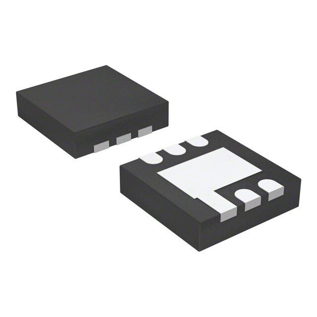
ICGOO在线商城 > 集成电路(IC) > PMIC - 稳压器 - 线性 > ISL9021AIRUWZ-T
- 型号: ISL9021AIRUWZ-T
- 制造商: Intersil
- 库位|库存: xxxx|xxxx
- 要求:
| 数量阶梯 | 香港交货 | 国内含税 |
| +xxxx | $xxxx | ¥xxxx |
查看当月历史价格
查看今年历史价格
ISL9021AIRUWZ-T产品简介:
ICGOO电子元器件商城为您提供ISL9021AIRUWZ-T由Intersil设计生产,在icgoo商城现货销售,并且可以通过原厂、代理商等渠道进行代购。 ISL9021AIRUWZ-T价格参考。IntersilISL9021AIRUWZ-T封装/规格:PMIC - 稳压器 - 线性, Linear Voltage Regulator IC Positive Fixed 1 Output 1.2V 250mA 6-UTDFN (1.6x1.6)。您可以下载ISL9021AIRUWZ-T参考资料、Datasheet数据手册功能说明书,资料中有ISL9021AIRUWZ-T 详细功能的应用电路图电压和使用方法及教程。
| 参数 | 数值 |
| 产品目录 | 集成电路 (IC) |
| 描述 | IC REG LDO 1.2V 0.25A 6UTDFN |
| 产品分类 | |
| 品牌 | Intersil |
| 数据手册 | |
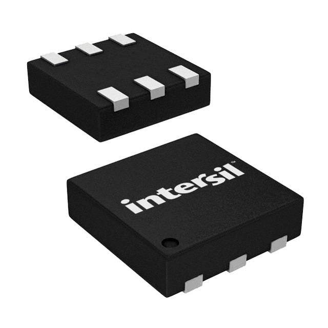
| 产品图片 |
|
| 产品型号 | ISL9021AIRUWZ-T |
| rohs | 无铅 / 符合限制有害物质指令(RoHS)规范要求 |
| 产品系列 | - |
| 供应商器件封装 | 6-UTDFN(1.6x1.6) |
| 其它名称 | ISL9021AIRUWZ-TCT |
| 包装 | 剪切带 (CT) |
| 安装类型 | 表面贴装 |
| 封装/外壳 | 6-UFDFN |
| 工作温度 | -40°C ~ 85°C |
| 标准包装 | 1 |
| 电压-跌落(典型值) | - |
| 电压-输入 | 1.5 V ~ 5.5 V |
| 电压-输出 | 1.2V |
| 电流-输出 | 250mA |
| 电流-限制(最小值) | 260mA |
| 稳压器拓扑 | 正,固定式 |
| 稳压器数 | 1 |


PDF Datasheet 数据手册内容提取
DATASHEET ISL9021A FN7845 250mA Single LDO with Low I , Low Noise and High PSRR LDO Rev 3.00 Q December 20, 2012 The ISL9021A is a single LDO, which provides high Features performance, low input voltage and high PSRR. It delivers guaranteed continuous 250mA load current and is stable with • High performance LDO with 250mA guaranteed continuous 1µF to 4.7µF of output capacitance (±30%) with an ESR range output current of 5m to 400m. • Input voltage range: 1.5V to 5.5V The input voltage range for the ISL9021A is between 1.5V to • Output voltage range: 1.2V to 3.3V 5.5V and the output voltage comes in many fixed voltage • High PSRR: 75dB @ 10kHz, 50dB @ 1MHz options with ±1.8% accuracy over-temperature, line and load ranges. The ISL9021A has typical PSRR of 75dB @ 10kHz and • Low quiescent current: 35µA 50dB @ 1MHz. • Dropout voltage: <150mV @ 250mA The reverse current protection feature prevents current from • Stable with 1µF to 4.7µF output capacitance (±30%) with an flowing back to the power source when the output voltage is ESR range of 5m to 400m pulled higher than the input. • ±1.8% output accuracy over-temperature/load/line The ISL9021A is offered in tiny 4-bump 0.975mmx1.155mm • Soft-start limits input current surge during enable WLCSP and 1.6mmx1.6mm 6 Ld µTDFN packages. • Current limit and overheat protection Related Literature • -40°C to +85°C operating temperature range • See FN6867, ISL9021 “250mA Single LDO with Low IQ, Low • Available in 0.975mmx1.155mm 4-bump WLCSP package Noise and High PSRR LDO” and 1.6mmx1.6mm 6 Ld µTDFN • Pb-free (RoHS compliant) Applications • PDAs, cell phones and smart phones • Portable instruments, MP3 players • Handheld devices including medical handheld ISL9021A VIN (1.5V TO 5.5V) VIN VO VOUT ON ENABLE EN GND OFF C1 C2 C1, C2: 1µF X5R CERAMIC CAPACITOR FIGURE 1. TYPICAL APPLICATION FN7845 Rev 3.00 Page 1 of 12 December 20, 2012
ISL9021A Block Diagram VIN PASS ELEMENT VOUT EN SHORT-CIRCUIT TEMP CONTROL PROTECTION SENSOR LOGIC THERMAL PROTECTION SOFT-START VOLTAGE AND + REFERENCE GENERATOR BANDGAP GND Pin Configurations Pin Descriptions ISL9021A (6 LD 1.6x1.6 µTDFN) PIN µTDFN WLCSP TOP VIEW NAME PIN # PIN # DESCRIPTION VIN 1 B1 IC Supply/LDO Input. Connect a 1µF VIN 1 6 VO capacitor to GND. NC 2, 5 - No Connect. NC 2 5 NC GND 4 A2 System ground pin. EN 3 4 GND EN 3 A1 LDO Enable. When this signal goes high, the LDO is turned on. ISL9021A VO, 6 B2 LDO Output. Connect a 1µF to 4.7µF (4 BALL 0.975x1.155 WLCSP) VOUT capacitor to GND. TOP VIEW PAD - - For µTDFN package option only. Connect it to the system ground. GND A2 B2 VOUT EN A1 B1 VIN FN7845 Rev 3.00 Page 2 of 12 December 20, 2012
ISL9021A Ordering Information PACKAGE PART NUMBER PART VO VOLTAGE TEMP RANGE Tape & Reel PKG. (Notes 1, 4) MARKING (V) (°C) (Pb-free) DWG. # ISL9021AIINZ-T (Note 2) 21AN 3.3 -40°C to +85°C 4 Ball 0.975x1.155 WLCSP W2x2.4 ISL9021AIIUZ-T (Note 2) 21AU 3.1 -40°C to +85°C 4 Ball 0.975x1.155 WLCSP W2x2.4 ISL9021AIIMZ-T (Note 2) 21AM 3.0 -40°C to +85°C 4 Ball 0.975x1.155 WLCSP W2x2.4 ISL9021AIIKZ-T (Note 2) 21AK 2.85 -40°C to +85°C 4 Ball 0.975x1.155 WLCSP W2x2.4 ISL9021AIIFZ-T (Note 2) 21AF 2.5 -40°C to +85°C 4 Ball 0.975x1.155 WLCSP W2x2.4 ISL9021AIICZ-T (Note 2) 21AC 1.8 -40°C to +85°C 4 Ball 0.975x1.155 WLCSP W2x2.4 ISL9021AIIBZ-T (Note 2) 21AB 1.5 -40°C to +85°C 4 Ball 0.975x1.155 WLCSP W2x2.4 ISL9021AIIWZ-T (Note 2) 21AW 1.2 -40°C to +85°C 4 Ball 0.975x1.155 WLCSP W2x2.4 ISL9021AIRUNZ-T (Note 3) V6 3.3 -40°C to +85°C 6 Ld µTDFN L6.1.6x1.6 ISL9021AIRUNZ-T7A (Note 3) V6 3.3 -40°C to +85°C 6 Ld µTDFN L6.1.6x1.6 ISL9021AIRUMZ-T (Note 3) V5 3.0 -40°C to +85°C 6 Ld µTDFN L6.1.6x1.6 ISL9021AIRUMZ-T7A (Note 3) V5 3.0 -40°C to +85°C 6 Ld µTDFN L6.1.6x1.6 ISL9021AIRUKZ-T (Note 3) V4 2.85 -40°C to +85°C 6 Ld µTDFN L6.1.6x1.6 ISL9021AIRUKZ-T7A (Note 3) V4 2.85 -40°C to +85°C 6 Ld µTDFN L6.1.6x1.6 ISL9021AIRUJZ-T (Note 3) V3 2.8 -40°C to +85°C 6 Ld µTDFN L6.1.6x1.6 ISL9021AIRUJZ-T7A (Note 3) V3 2.8 -40°C to +85°C 6 Ld µTDFN L6.1.6x1.6 ISL9021AIRUFZ-T (Note 3) V2 2.5 -40°C to +85°C 6 Ld µTDFN L6.1.6x1.6 ISL9021AIRUFZ-T7A (Note 3) V2 2.5 -40°C to +85°C 6 Ld µTDFN L6.1.6x1.6 ISL9021AIRUCZ-T (Note 3) V1 1.8 -40°C to +85°C 6 Ld µTDFN L6.1.6x1.6 ISL9021AIRUCZ-T7A (Note 3) V1 1.8 -40°C to +85°C 6 Ld µTDFN L6.1.6x1.6 ISL9021AIRUBZ-T (Note 3) V0 1.5 -40°C to +85°C 6 Ld µTDFN L6.1.6x1.6 ISL9021AIRUBZ-T7A (Note 3) V0 1.5 -40°C to +85°C 6 Ld µTDFN L6.1.6x1.6 ISL9021AIRUWZ-T (Note 3) V7 1.2 -40°C to +85°C 6 Ld µTDFN L6.1.6x1.6 ISL9021AIRUWZ-T7A (Note 3) V7 1.2 -40°C to +85°C 6 Ld µTDFN L6.1.6x1.6 ISL9021AIRUYZ-T (Note 3) V8 0.9 -40°C to +85°C 6 Ld µTDFN L6.1.6x1.6 ISL9021AIRUYZ-T7A (Note 3) V8 0.9 -40°C to +85°C 6 Ld µTDFN L6.1.6x1.6 ISL9021AIINZ-EVZ Evaluation Board for ISL9021AIINZ ISL9021AIIUZ-EVZ Evaluation Board for ISL9021AIIUZ ISL9021AIIMZ-EVZ Evaluation Board for ISL9021AIIMZ ISL9021AIIKZ-EVZ Evaluation Board for ISL9021AIIKZ ISL9021AIIFZ-EVZ Evaluation Board for ISL9021AIIFZ ISL9021AIICZ-EVZ Evaluation Board for ISL9021AIICZ ISL9021AIIBZ-EVZ Evaluation Board for ISL9021AIIBZ ISL9021AIIWZ-EVZ Evaluation Board for ISL9021AIIWZ ISL9021AIRUNZ-EVZ Evaluation Board for ISL9021AIRUNZ ISL9021AIRUMZ-EVZ Evaluation Board for ISL9021AIRUMZ ISL9021AIRUKZ-EVZ Evaluation Board for ISL9021AIRUKZ ISL9021AIRUJZ-EVZ Evaluation Board for ISL9021AIRUJZ FN7845 Rev 3.00 Page 3 of 12 December 20, 2012
ISL9021A Ordering Information (Continued) PACKAGE PART NUMBER PART VO VOLTAGE TEMP RANGE Tape & Reel PKG. (Notes 1, 4) MARKING (V) (°C) (Pb-free) DWG. # ISL9021AIRUFZ-EVZ Evaluation Board for ISL9021AIRUFZ ISL9021AIRUCZ-EVZ Evaluation Board for ISL9021AIRUCZ ISL9021AIRUBZ-EVZ Evaluation Board for ISL9021AIRUBZ ISL9021AIRUWZ-EVZ Evaluation Board for ISL9021AIRUWZ ISL9021AIRUYZ-EVZ Evaluation Board for ISL9021AIRUYZ NOTES: 1. Please refer to TB347 for details on reel specifications. 2. These Intersil Pb-free WLCSP and BGA packaged products employ special Pb-free material sets; molding compounds/die attach materials and SnAgCu - e1 solder ball terminals, which are RoHS compliant and compatible with both SnPb and Pb-free soldering operations. Intersil Pb-free WLCSP and BGA packaged products are MSL classified at Pb-free peak reflow temperatures that meet or exceed the Pb-free requirements of IPC/JEDEC J STD-020. 3. These Intersil Pb-free plastic packaged products employ special Pb-free material sets; molding compounds/die attach materials and NiPdAu plate - e4 termination finish, which is RoHS compliant and compatible with both SnPb and Pb-free soldering operations. Intersil Pb-free products are MSL classified at Pb-free peak reflow temperatures that meet or exceed the Pb-free requirements of IPC/JEDEC J STD-020. 4. For Moisture Sensitivity Level (MSL), please see device information page for ISL9021A. For more information on MSL please see techbrief TB363. FN7845 Rev 3.00 Page 4 of 12 December 20, 2012
ISL9021A Absolute Maximum Ratings Thermal Information Supply Voltage (VIN). . . . . . . . . . . . . . . . . . . . . . . . . . . . . . . . . . . . . . . . +6.5V Thermal Resistance (Typical) JA (°C/W) JC (°C/W) All Other Pins . . . . . . . . . . . . . . . . . . . . . . . . . . . . . . . . . . -0.3 to (VIN + 0.3)V 4 Ball WLCSP (Note 5). . . . . . . . . . . . . . . . . 135.64 N/A 6 Lead µTDFN (Notes 6, 7) . . . . . . . . . . . . . 230 93 Recommended Operating Conditions Junction Temperature Range . . . . . . . . . . . . . . . . . . . . . . .-40°C to +125°C Operating Temperature Range . . . . . . . . . . . . . . . . . . . . . .-40°C to +85°C Ambient Temperature Range (TA) . . . . . . . . . . . . . . . . . . . .-40°C to +85°C Storage Temperature Range. . . . . . . . . . . . . . . . . . . . . . . .-65°C to +150°C Supply Voltage (VIN). . . . . . . . . . . . . . . . . . . . . . . . . . . . . . . . . . . . 1.5 to 5.5V Pb-Free Reflow Profile . . . . . . . . . . . . . . . . . . . . . . . . . . . . . . . see link below ESD Rating http://www.intersil.com/pbfree/Pb-FreeReflow.asp Human Body Model. . . . . . . . . . . . . . . . . . . . . . . . . . . . . . . . . . . . . .5000V Machine Model . . . . . . . . . . . . . . . . . . . . . . . . . . . . . . . . . . . . . . . . . 250V Charged Device Model . . . . . . . . . . . . . . . . . . . . . . . . . . . . . . . . . . .2200V Latch-Up Passed at +85°C . . . . . . . . . . . . . . . . . . . . . . . . . . . . . . . . . 100mA CAUTION: Do not operate at or near the maximum ratings listed for extended periods of time. Exposure to such conditions may adversely impact product reliability and result in failures not covered by warranty. NOTES: 5. JA is measured in free air with the component mounted on a high effective thermal conductivity test board with “direct attach” features. See Tech Brief TB379. 6. JA is measured with the component mounted on a high effective thermal conductivity test board in free air. See Tech Brief TB379 for details. 7. For JC, the “case temp” location is taken at the package top center. Electrical Specifications TA = -40°C to +85°C; VIN = (VO + 0.5V) to 5.5V with a minimum VIN of 1.5V; CIN = 1µF; CO = 1µF. Boldface limits apply over the operating temperature range, -40°C to +85°C. MIN MAX PARAMETER SYMBOL TEST CONDITIONS (Note 10) TYP (Note 10) UNIT DC CHARACTERISTICS Supply Voltage VIN 1.5 5.5 V VIN Undervoltage Lockout VUVLO+ VIN Rising 1.425 1.5 V Threshold VUVLO- VIN Falling 1.3 1.375 V Ground Current IDD Output Enabled; IO = 0; VIN = 1.5V to 5.5V 35 50 µA Shutdown Current IDDS VIN = 5.5V, EN = Low, IO = 0 0.1 1.0 µA Output Voltage Accuracy VIN = VO + 0.5V to 5.5V, IO = 1mA to 250mA, TJ = +25°C -0.8 +0.8 % VIN = VO + 0.5V to 5.5V, IO = 1mA to 250mA, TJ = -40°C to +125°C -1.8 +1.8 % Maximum Output Current IMAX Continuous 250 mA Internal Current Limit ILIM 260 mA Dropout Voltage (Notes 8, 9) VDO IO = 250mA; VO > 1.8V 150 250 mV Thermal Shutdown Temperature TSD 160 °C Thermal Shutdown Hysteresis 20 °C AC CHARACTERISTICS Ripple Rejection (Note 8) VIN = 4.5V, VO = 3.3V @ 1kHz 60 dB VIN = 4.5V, VO = 3.3V @ 10kHz 75 dB VIN = 4.5V, VO = 3.3V @ 1MHz 50 dB Output Noise Voltage (Note 8) VIN = 4.2V, TA = +25°C, BW = 10Hz to 100kHz, IO = 10mA 8.5*VO µVRMS DEVICE START-UP CHARACTERISTICS Device Enable Time tEN Time from assertion of the EN pin to when the output voltage 250 600 µs reaches 95% of the VO (nom) LDO Soft-start Ramp Rate tSSR Slope of linear portion of LDO output voltage ramp during start-up 30 60 µs/V FN7845 Rev 3.00 Page 5 of 12 December 20, 2012
ISL9021A Electrical Specifications TA = -40°C to +85°C; VIN = (VO + 0.5V) to 5.5V with a minimum VIN of 1.5V; CIN = 1µF; CO = 1µF. Boldface limits apply over the operating temperature range, -40°C to +85°C. (Continued) MIN MAX PARAMETER SYMBOL TEST CONDITIONS (Note 10) TYP (Note 10) UNIT EN LOGIC CHARACTERISTICS Input Low Voltage VIL 0.4 V Input High Voltage VIH 1.1 V Input Leakage Current IIL, IIH 0.1 µA NOTES: 8. Limits established by characterization and are not production tested. 9. Dropout voltage is measured as VIN - VO, when VO is 4% lower than the value of VO 10. Parameters with MIN and/or MAX limits are 100% tested at +25°C, unless otherwise specified. Temperature limits established by characterization and are not production tested. Typical Operating Performance 45 45 T = ROOM TEMP T = +45°C T = +85°C T = ROOM TEMP T = +45°C T = +85°C A) 40 A) 40 µ µ T ( 35 T ( 35 N N E 30 E 30 R R CUR 25 T = 0°C CUR 25 T = 0°C T 20 T 20 N T = -25°C N T = -25°C CE 15 T = -40°C CE 15 T = -40°C S S E 10 E 10 UI UI Q 5 Q 5 0 0 1.5 2.5 3.5 4.5 5.5 1.5 2.5 3.5 4.5 5.5 INPUT VOLTAGE (V) INPUT VOLTAGE (V) FIGURE 2. QUIESCENT CURRENT vs INPUT VOLTAGE FIGURE 3. QUIESCENT CURRENT vs INPUT VOLTAGE (VOUT = 0.9V) (VOUT = 1.85V) 50 1.95 T = ROOM TEMP T = +45°C T = +85°C µA) 40 1.90 +85°C +25°C NT ( 1.85 E 30 R UR T = 0°C V) 1.80 T C 20 T = -40°C T = -25°C Vo ( 1.75 -40°C N SCE 10 1.70 E QUI 0 1.65 -10 1.60 3.5 4.0 4.5 5.0 5.5 6.0 0 50 100 150 200 250 300 INPUT VOLTAGE (V) Io (mA) FIGURE 4. QUIESCENT CURRENT vs INPUT VOLTAGE FIGURE 5. LOAD REGULATION vs TEMPERATURE (VOUT = 3.3V) (VOUT=1.85V) FN7845 Rev 3.00 Page 6 of 12 December 20, 2012
ISL9021A Typical Operating Performance (Continued) 2.00 3.5 1.95 +25°C 3.4 +25°C 1.90 +85°C 1.85 3.3 Vo (V) 11..7850 +85°C -40°C Vo (V) 33..12 -40°C 1.70 1.65 3.0 1.60 2.9 1.55 1.50 2.8 2.5 3.5 4.5 5.5 6.5 0 50 100 150 200 250 300 VIN(V) Io (mA) FIGURE 6. LINE REGULATION vs TEMPERATURE (VOUT=1.85V) FIGURE 7. LOAD REGULATION vs TEMPERATURE (VOUT=3.3V) 3.50 1.05 3.45 1.00 3.40 +25°C 0.95 3.35 +25°C +85°C +85°C 0.90 3.30 V) V) 0.85 Vo ( 33..2205 -40°C Vo ( 0.80 -40°C 3.15 0.75 3.10 0.70 3.05 0.65 3.00 0.60 3.5 4.0 4.5 5.0 5.5 6.0 0 50 100 150 200 250 300 VIN (V) Io (mA) FIGURE 8. LINE REGULATION vs TEMPERATURE (VOUT=3.3V) FIGURE 9. LOAD REGULATION vs TEMPERATURE (VOUT=0.9V) VIN = 2.7V 1.00 VOUT = 1.85V COUT = 1µF 0.95 VOUT +25°C +85°C 0.90 V) o ( 0.85 -40°C V 0.80 0.75 IOUT 0.70 IOUT = 1mA TO 250mA 3.0 3.5 4.0 4.5 5.0 5.5 6.0 VIN (V) FIGURE 10. LINE REGULATION vs TEMPERATURE (VOUT=0.9V) FIGURE 11. LOAD TRANSIENT RESPONSE FN7845 Rev 3.00 Page 7 of 12 December 20, 2012
ISL9021A Typical Operating Performance (Continued) VIN = 2.7V COUT = 4.7µF VOUT = 1.85V VOUT IOUT IOUT = 1mA TO 250mA FIGURE 12. LOAD TRANSIENT RESPONSE FIGURE 13. ENABLE FUNCTION (VIN = 3.6V, VOUT = 1.85V, COUT 1µF) -20 VIN = 4.5VDC + 50mVAC -30 COUT = 1µF -40 IO = 10mA B) d -50 R ( R -60 S P -70 IO = 0A -80 -90 100 1k 10k 100k 1M FREQUENCY (Hz) FIGURE 14. POWER SUPPLY REJECTION vs FREQUENCY FN7845 Rev 3.00 Page 8 of 12 December 20, 2012
ISL9021A Functional Description The ISL9021A’s reverse current protection is intended to block reverse conduction if output voltage is higher than input voltage. The ISL9021A is a high performance low-dropout regulator (LDO) with 250mA sourcing capability. The extra low ground current Input and Output Capacitors makes this part a good choice for handheld product applications. The ISL9021A provides a linear regulator that has low quiescent The device also incorporates overcurrent, thermal shutdown, current, fast transient response, and overall stable operation reverse current protections, and soft-start features. across the recommended operating conditions. A ceramic Thermal shutdown protects the device against overheating. capacitor (X5R or X7R) with a capacitance of 1µF to 4.7µF with Soft-start limits the start-up input current surges. In some an ESR up to 400m is suitable for the ISL9021A to maintain its applications, the output voltage may be externally pulled higher output stability. The ground connection of the output capacitor than the input, or the input voltage could be connected to ground, should be routed directly to the GND pin of the device, and also or connected to some voltage lower than the output side. The placed close to the IC. Similarly for the input capacitor, usually a ISL9021A features reverse current protection; that can block the 1µF ceramic capacitor (X5R or 7R) is suitable for most cases, but reverse current from output to input. if a large, fast rising load transient condition is expected, a higher value input capacitor may be necessary to achieve satisfactory Enable Control performance. The ISL9021A has an enable pin. When EN is low, the IC is in Board Layout Recommendations shutdown mode. In this condition, all on-chip circuits are off, and the device draws minimum current, typically less than A good PCB layout is an important step to achieve good 0.1µA(typ). Driving this pin high will turn on the device. performance. It is recommended to design the board with separate ground planes for input and output, and connect both LDO Protections ground planes at the GND pin of the IC. Consideration should be taken when placing the components and routing the trace to The ISL9021A offers several protection functions, making it ideal for minimize the ground impedance, and keep the parasitic use in battery-powered applications. The ISL9021A provides inductance low. Usually the input/output capacitors should be short-circuit protection by limiting the output current at current limit placed as close to the IC as possible with a good ground of 260mA (min). If the short circuit lasts long enough, the die connection. temperature increases, and the over-temperature protection circuit will shut down the output. When the die temperature reaches about +145°C, thermal protection starts to work with output being loaded with at least 50mA. Once the die temperature drops to about +110°C, the LDO will resume operation beginning with a soft-start. FN7845 Rev 3.00 Page 9 of 12 December 20, 2012
ISL9021A Revision History The revision history provided is for informational purposes only and is believed to be accurate, but not warranted. Please go to web to make sure you have the latest revision. DATE REVISION CHANGE December 17, 2012 FN7845.3 Added evaluation boards and ISL9021AIIUZ-T to “Ordering Information” on page3. December 2, 2011 FN7845.2 Changed CSP package dimension from “2mmx2mm” to “0.975mmx1.155mm” on page1 to page3. October 7, 2011 FN7845.1 Updated “Ordering Information” on page3 by adding ISL9021AIRUYZ-T and ISL9021AIRUYZ-T7A parts. Made corrections to part markings and added -T7A parts. May 27, 2011 FN7845.0 Initial Release About Intersil Intersil Corporation is a leader in the design and manufacture of high-performance analog, mixed-signal and power management semiconductors. The company's products address some of the fastest growing markets within the industrial and infrastructure, personal computing and high-end consumer markets. For more information about Intersil or to find out how to become a member of our winning team, visit our website and career page at www.intersil.com. For a complete listing of Applications, Related Documentation and Related Parts, please see the respective product information page. Also, please check the product information page to ensure that you have the most updated datasheet: ISL9021A To report errors or suggestions for this datasheet, please go to: www.intersil.com/askourstaff Reliability reports are available from our website at: http://rel.intersil.com/reports/search.php © Copyright Intersil Americas LLC 2011-2012. All Rights Reserved. All trademarks and registered trademarks are the property of their respective owners. For additional products, see www.intersil.com/en/products.html Intersil products are manufactured, assembled and tested utilizing ISO9001 quality systems as noted in the quality certifications found at www.intersil.com/en/support/qualandreliability.html Intersil products are sold by description only. Intersil may modify the circuit design and/or specifications of products at any time without notice, provided that such modification does not, in Intersil's sole judgment, affect the form, fit or function of the product. Accordingly, the reader is cautioned to verify that datasheets are current before placing orders. Information furnished by Intersil is believed to be accurate and reliable. However, no responsibility is assumed by Intersil or its subsidiaries for its use; nor for any infringements of patents or other rights of third parties which may result from its use. No license is granted by implication or otherwise under any patent or patent rights of Intersil or its subsidiaries. For information regarding Intersil Corporation and its products, see www.intersil.com FN7845 Rev 3.00 Page 10 of 12 December 20, 2012
ISL9021A Package Outline Drawing L6.1.6x1.6 6 LEAD ULTRA THIN DUAL FLAT NO-LEAD COL PLASTIC PACKAGE (UTDFN COL) Rev 1, 11/07 2X 1.00 1.60 A PIN #1 INDEX AREA 6 6 4X 0.50 PIN 1 INDEX AREA B 1 3 5X 0 . 40 ± 0 . 1 1X 0.5 ±0.1 1.60 (4X) 0.15 6 4 0.10M C AB TOP VIEW 4 0.25 +0.05 / -0.07 BOTTOM VIEW ( 6X 0 . 25 ) SEE DETAIL "X" ( 1X 0 .70 ) 0 . 55 MAX 0.10 C C BASE PLANE SEATING PLANE ( 1 . 4 ) 0.08 C SIDE VIEW 0 . 2 REF C ( 5X 0 . 60 ) 0 . 00 MIN. 0 . 05 MAX. ( 4X 0 . 5 ) DETAIL "X" TYPICAL RECOMMENDED LAND PATTERN NOTES: 1. Dimensions are in millimeters. Dimensions in ( ) for Reference Only. 2. Dimensioning and tolerancing conform to AMSE Y14.5m-1994. 3. Unless otherwise specified, tolerance : Decimal ± 0.05 4. Dimension b applies to the metallized terminal and is measured between 0.15mm and 0.30mm from the terminal tip. 5. Tiebar shown (if present) is a non-functional feature. 6. The configuration of the pin #1 identifier is optional, but must be located within the zone indicated. The pin #1 identifier may be either a mold or mark feature. FN7845 Rev 3.00 Page 11 of 12 December 20, 2012
ISL9021A Wafer Level Chip Scale Package W2x2.4 (WLCSP 0.4mm Ball Pitch) 2x2 ARRAY 4 BALL WAFER LEVEL CHIP SCALE PACKAGE SYMBOL MILLIMETERS D A 0.44 Min, 0.495 Nom, 0.55 Max A1 0.190 ±0.030 A2 0.305 ±0.025 E b 0.270 ±0.030 D 1.155 ±0.020 D1 0.400 BASIC PIN 1 TOP VIEW E 0.975 ±0.020 E1 0.400 BASIC e 0.400 BASIC SD 0.200 BASIC SE 0.00 BASIC NUMBER OF BUMPS: 4 Rev. 2 6/08 A2 A NOTES: A1 1. All dimensions are in millimeters. b SIDE VIEW e ( D1 ) 2 SE e ( E1 ) 1 B A b SD BOTTOM VIEW FN7845 Rev 3.00 Page 12 of 12 December 20, 2012
 Datasheet下载


