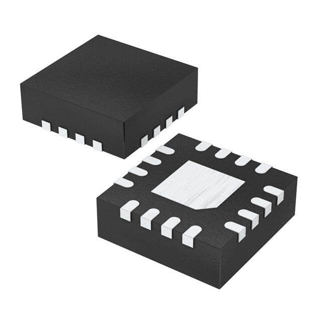
ICGOO在线商城 > 集成电路(IC) > PMIC - 稳压器 - DC DC 开关稳压器 > ISL8502IRZ-T
- 型号: ISL8502IRZ-T
- 制造商: Intersil
- 库位|库存: xxxx|xxxx
- 要求:
| 数量阶梯 | 香港交货 | 国内含税 |
| +xxxx | $xxxx | ¥xxxx |
查看当月历史价格
查看今年历史价格
ISL8502IRZ-T产品简介:
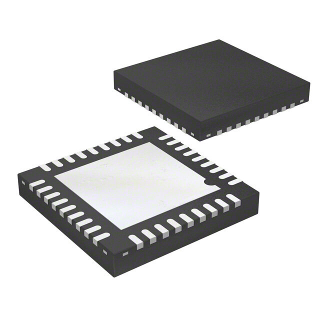
ICGOO电子元器件商城为您提供ISL8502IRZ-T由Intersil设计生产,在icgoo商城现货销售,并且可以通过原厂、代理商等渠道进行代购。 ISL8502IRZ-T价格参考。IntersilISL8502IRZ-T封装/规格:PMIC - 稳压器 - DC DC 开关稳压器, Buck Switching Regulator IC Positive Adjustable 0.6V 1 Output 2A 24-VFQFN Exposed Pad。您可以下载ISL8502IRZ-T参考资料、Datasheet数据手册功能说明书,资料中有ISL8502IRZ-T 详细功能的应用电路图电压和使用方法及教程。
| 参数 | 数值 |
| 产品目录 | 集成电路 (IC) |
| 描述 | IC REG BUCK SYNC ADJ 2A 24QFN |
| 产品分类 | |
| 品牌 | Intersil |
| 数据手册 | |
| 产品图片 |
|
| 产品型号 | ISL8502IRZ-T |
| PCN设计/规格 | |
| PWM类型 | 电压模式 |
| rohs | 无铅 / 符合限制有害物质指令(RoHS)规范要求 |
| 产品系列 | - |
| 产品目录页面 | |
| 供应商器件封装 | 24-QFN(4x4) |
| 其它名称 | ISL8502IRZ-TCT |
| 包装 | 剪切带 (CT) |
| 同步整流器 | 是 |
| 安装类型 | 表面贴装 |
| 封装/外壳 | 24-VFQFN 裸露焊盘 |
| 工作温度 | -40°C ~ 85°C |
| 标准包装 | 1 |
| 电压-输入 | 5.5 V ~ 14 V |
| 电压-输出 | 0.6 V ~ 14 V |
| 电流-输出 | 2A |
| 类型 | 降压(降压) |
| 输出数 | 1 |
| 输出类型 | 可调式 |
| 频率-开关 | 500kHz ~ 1.2MHz |

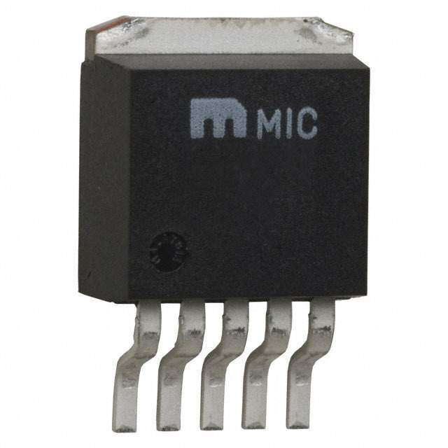

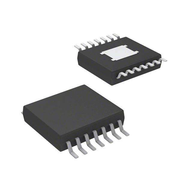

PDF Datasheet 数据手册内容提取
DATASHEET ISL8502 FN6389 2A Synchronous Buck Regulator with Integrated MOSFETs Rev 2.00 June 29, 2010 The ISL8502 is a synchronous buck controller with internal Features MOSFETs packaged in a small 4mmx4mm QFN package. • Up to 2A Continuous Output Current The ISL8502 can support a continuous load of 2A and has a very wide input voltage range. With the switching MOSFETs • Integrated MOSFETs for Small Regulator Footprint integrated into the IC, the complete regulator footprint can • Adjustable Switching Frequency, 500kHz to 1.2MHz be very small and provide a much more efficient solution than a linear regulator. • Tight Output Voltage Regulation, ±1% Over-Temperature The ISL8502 is capable of stand alone operation or it can be • Wide Input Voltage Range, 5V ±10% or 5.5V to 14V used in a master slave combination for multiple outputs that • Wide Output Voltage Range, from 0.6V are derived from the same input rail. Multiple slave channels • Simple Single-Loop Voltage-Mode PWM Control Design (up to six) can be synchronized. This method minimizes the EMI and beat frequencies effect with multi-channel • Input Voltage Feed-Forward for Constant Modulator Gain operation. • Fast PWM Converter Transient Response The switching PWM controller drives two internal N-Channel • Lossless rDS(ON) High Side and Low Side Overcurrent MOSFETs in a synchronous-rectified buck converter Protection topology. The synchronous buck converter uses voltage-mode control with fast transient response. The • Undervoltage Detection switching regulator provides a maximum static regulation • Integrated Thermal Shutdown Protection tolerance of ±1% over line, load, and temperature ranges. • Power-Good Indication The output is user-adjustable by means of external resistors down to 0.6V. • Adjustable Soft-Start The output is monitored for undervoltage events. The • Start-Up with Pre-Bias Output switching regulator also has overcurrent protection. Thermal • Pb-free (RoHS Compliant) shutdown is integrated. The ISL8502 features a bi-directional Enable pin that allows the part to pull the enable pin low Applications during fault detection. • Point of Load Applications Pinout ISL8502 • Graphics Cards - GPU and Memory Supplies (24 LD QFN) • ASIC Power Supplies TOP VIEW C T • Embedded Processor and I/O supplies VCC PVC BOO VIN VIN VIN • DSP Supplies 24 23 22 21 20 19 Ordering Information PGOOD 1 18 VIN PART TEMP. SGND 2 17 PHASE NUMBER PART RANGE PACKAGE PKG. EN 3 16 PHASE (Note) MARKING (°C) (Pb-free) DWG. # GND SYNCH 4 25 15 PHASE ISL8502IRZ* 85 02IRZ -40 to +85 24 Ld 4x4 QFN L24.4x4D *Add “-T” suffix for tape and reel. Please refer to TB347 for details on M/S 5 14 PHASE reel specifications. FS 6 13 PGND NOTE: These Intersil Pb-free plastic packaged products employ special Pb-free material sets, molding compounds/die attach 7 8 9 10 11 12 materials, and 100% matte tin plate plus anneal (e3 termination finish, P B S D D D which is RoHS compliant and compatible with both SnPb and Pb-free OM F S GN GN GN soldering operations). Intersil Pb-free products are MSL classified at C P P P Pb-free peak reflow temperatures that meet or exceed the Pb-free requirements of IPC/JEDEC J STD-020. FN6389 Rev 2.00 Page 1 of 19 June 29, 2010
JuFN Block Diagram IS ne 2638 L850 99 2 , 2R 0e 1v 0 2 PVCC VCC SS PGOOD VIN (x4) .0 0 VIN OC PVCC MONITOR SERIES POR 30A REGULATOR MONITOR SGND BIAS PVCC BOOT EN FAULT MONITORING GATE DRIVE AND ADAPTIVE PHASE (x4) VOLTAGE SHOOT THRU SYNCH MONITOR PROTECTION CLOCK M/S AND OSCILLATOR GENERATOR OC 0.6V FS MONITOR REFERENCE FB COMP PGND (x4) P a g e 2 o f 1 9
ISL8502 Typical Application Schematics POWER GOOD PGOOD VIN VIN + ENABLE EN 5.5V TO 14V SYNCH M/S BOOT VCC PVCC ISL8502 VOUT PHASE SS + PGND FS FB SGND COMP FIGURE 1. STAND ALONE REGULATOR: VIN 5.5V TO 14V VIN 4.5V TO 5.5V POWER GOOD PGOOD VIN ENABLE EN + PVCC VCC BOOT SS ISL8502 VOUT PHASE + SYNCH PGND M/S FS FB SGND COMP FIGURE 2. STAND ALONE REGULATOR: VIN 4.5V TO 5.5V FN6389 Rev 2.00 Page 3 of 19 June 29, 2010
ISL8502 ISL8502 With Multiple Slaved Channels VIN MASTER PVCC M/S VIN SS FS VOUT1 SYNCH PHASE + RT EN GND ISL8502 ENABLE M/S VIN FS 5k VOUT2 RT SYNCH PHASE + EN GND ISL8502 SLAVE M/S VIN FS 5k VOUTN RT SYNCH PHASE + EN GND ISL8502 SLAVE FN6389 Rev 2.00 Page 4 of 19 June 29, 2010
ISL8502 Absolute Maximum Ratings Thermal Information VIN. . . . . . . . . . . . . . . . . . . . . . . . . . . . . . . . . GND - 0.3V to +16.5V Thermal Resistance JA (°C/W) JC (°C/W) VCC. . . . . . . . . . . . . . . . . . . . . . . . . . . . . . . . . GND - 0.3V to +6.0V QFN Package (Notes 1, 2) . . . . . . . . . 39 2.5 Absolute Boot Voltage, VBOOT . . . . . . . . . . . . . . . . . . . . . . . +22.0V Maximum Junction Temperature (Plastic Package) . . . . . . +150°C Upper Driver Supply Voltage, VBOOT - VPHASE. . . . . . . . . . . +6.0V Maximum Storage Temperature Range. . . . . . . . . -65°C to +150°C All other Pins . . . . . . . . . . . . . . . . . . . . . GND - 0.3V to VCC + 0.3V Pb-free Reflow Profile . . . . . . . . . . . . . . . . . . . . . . . . .see link below http://www.intersil.com/pbfree/Pb-FreeReflow.asp Recommended Operating Conditions Supply Voltage on VIN. . . . . . . . . . . . . . . . . . . . . . . . . . 5.5V to 14V Ambient Temperature Range. . . . . . . . . . . . . . . . . . -40°C to +85°C Junction Temperature Range. . . . . . . . . . . . . . . . . -40°C to +125°C CAUTION: Do not operate at or near the maximum ratings listed for extended periods of time. Exposure to such conditions may adversely impact product reliability and result in failures not covered by warranty. NOTES: 1. JA is measured in free air with the component mounted on a high effective thermal conductivity test board with “direct attach” features. See Tech Brief TB379. 2. For JC, the “case temp” location is the center of the exposed metal pad on the package underside. 3. Minimum VIN can operate below 5.5V as long as VCC is greater than 4.5V. 4. Maximum VIN can be higher than 14V voltage stress across the upper and lower do not exceed 15.5V in all conditions. 5. Circuit requires 150ns minimum on time to detect overcurrent condition. 6. Limits established by characterization and are not production tested. 7. Parameters with MIN and/or MAX limits are 100% tested at +25°C, unless otherwise specified. Temperature limits established by characterization and are not production tested. Electrical Specifications Refer to Block and Simplified Power System Diagrams and Typical Application Schematics. Operating Conditions Unless Otherwise Noted: VIN = 12V, or VCC = 5V ±10%, TA = -40°C to +85°C. Typical are at TA=+25°C. MIN MAX PARAMETER SYMBOL TEST CONDITIONS (Note 7) TYP (Note 7) UNITS VIN SUPPLY Input Voltage Range VIN 5.5 14 V (Note 3) (Note 4) VIN tied to VCC 4.5 5.5 V Input Operating Supply Current IQ VFB = 1.0V 7 mA Input Standby Supply Current IQ_SBY EN tied to GND, VIN = 14V 1.25 2 mA SERIES REGULATOR VCC Voltage VPVCC VIN > 5.6V 4.5 5.0 5.5 V Maximum Output Current IPVCC VIN = 12V 50 mA VCC Current Limit VIN = 12V, VCC shorted to PGND 300 mA POWER-ON RESET Rising VCC POR Threshold 4.2 4.4 4.49 V Falling VCC POR Threshold 3.85 4.0 4.10 V ENABLE Rising Enable Threshold Voltage VEN_Rising 2.7 V Falling Enable Threshold Voltage VEN_Fall 2.3 V Enable Sinking Current IEN 500 µA OSCILLATOR FN6389 Rev 2.00 Page 5 of 19 June 29, 2010
ISL8502 Electrical Specifications Refer to Block and Simplified Power System Diagrams and Typical Application Schematics. Operating Conditions Unless Otherwise Noted: VIN = 12V, or VCC = 5V ±10%, TA = -40°C to +85°C. Typical are at TA=+25°C. (Continued) MIN MAX PARAMETER SYMBOL TEST CONDITIONS (Note 7) TYP (Note 7) UNITS PWM Frequency fOSC RT = 96k 400 500 600 kHz RT = 40k 960 1200 1440 kHz FS pin tied to VCC 800 kHz Ramp Amplitude VOSC VIN = 14V 1.0 V Ramp Amplitude VOSC VIN = 5V 0.470 V Modulator Gain VVIN/VOSC By Design 8 - Maximum Duty Cycle DMAX fOSC = 500kHz 88 % Maximum Duty Cycle DMAX fOSC = 1.2MHz 76 % REFERENCE VOLTAGE Reference Voltage VREF 0.600 V System Accuracy -1.0 +1.0 % FB Pin Bias Current ±80 ±200 nA SOFT-START Soft-Start Current ISS 20 30 40 µA Enable Soft-Start Threshold 0.8 1.0 1.2 V Enable Soft-Start Threshold Hysteresis 12 mV Enable Soft-Start Voltage High 2.8 3.2 3.8 V ERROR AMPLIFIER DC Gain 88 dB Gain-Bandwidth Product GBWP 15 MHz Maximum Output Voltage 3.9 4.4 V Slew Rate SR 5 V/µs INTERNAL MOSFETS Upper MOSFET rDS(ON) rDS_Upper VCC = 5V 180 m Lower MOSFET rDS(ON) rDS_Lower VCC = 5V 90 m PGOOD PGOOD Threshold VFB/VREF Rising Edge Hysteresis 1% 107 111 115 % Falling Edge Hysteresis 1% 86 90 93 % PGOOD Rising Delay tPGOOD_DELAY fOSC = 500kHz 250 ms PGOOD Leakage Current VPGOOD = 5.5V 5 µA PGOOD Low Voltage VPGOOD 0.10 V PGOOD Sinking Current IPGOOD 0.5 mA PROTECTION Positive Current Limit IPOC_peak IOC from VIN to PHASE (Notes 5, 6) 2.1 3.5 4.5 A (TA=0°C to +85°C) IOC from VIN to PHASE (Notes 5, 6) 2.0 3.4 4.0 A (TA=-40°C to +0°C) FN6389 Rev 2.00 Page 6 of 19 June 29, 2010
ISL8502 Electrical Specifications Refer to Block and Simplified Power System Diagrams and Typical Application Schematics. Operating Conditions Unless Otherwise Noted: VIN = 12V, or VCC = 5V ±10%, TA = -40°C to +85°C. Typical are at TA=+25°C. (Continued) MIN MAX PARAMETER SYMBOL TEST CONDITIONS (Note 7) TYP (Note 7) UNITS Negative Current Limit INOC_peak IOC from PHASE to PGND (Notes 5, 6) 2.2 3.0 3.5 A (TA=0°C to +85°C) IOC from PHASE to PGND (Notes 5, 6) 1.9 2.8 3.7 A (TA=-40°C to +85°C) Undervoltage Level VFB/VREF 76 80 84 % Thermal Shutdown Setpoint TSD 150 °C Thermal Recovery Setpoint TSR 130 °C Typical Performance Curves VIN = 12V, VOUT = 2.5V, IO = 2A, fs = 500kHz, L = 4.7µH, CIN = 20µF, COUT = 100µF + 22µF, TA=+25° C, unless otherwise noted. 100 100 90 90 %) 80 %) 80 Y ( Y ( CIENC 70 VOUT = 1.8V VOUT = 2.5V CIENC 70 VOUT = 3.3VVOUT = 5.0V FFI VOUT = 3.3V FFI VOUT = 2.5V E 60 E 60 VOUT = 1.8V 50 50 40 40 0.0 0.5 1.0 1.5 2.0 2.5 0.0 0.5 1.0 1.5 2.0 2.5 OUTPUT LOAD (A) OUTPUT LOAD (A) FIGURE 3. EFFICIENCY vs LOAD (VIN = 5V) FIGURE 4. EFFICIENCY vs LOAD (VIN = 12V) 0.6026 1.206 14VIN 0.6025 1.205 V) 0.6024 V) E ( E ( 1.204 G G OLTA 0.6023 14VIN OLTA 1.203 9VIN V V T 0.6022 T U U P P T T 1.202 OU 0.6021 9VIN OU 5VIN 1.201 0.6020 5VIN 0.6019 1.200 0 1 2 0 1 2 OUTPUT LOAD (A) OUTPUT LOAD (A) FIGURE 5. VOUT REGULATION vs LOAD (VOUT = 0.6V, 500kHz) FIGURE 6. VOUT REGULATION vs LOAD (VOUT = 1.2V, 500kHz) FN6389 Rev 2.00 Page 7 of 19 June 29, 2010
ISL8502 Typical Performance Curves VIN = 12V, VOUT = 2.5V, IO = 2A, fs = 500kHz, L = 4.7µH, CIN = 20µF, COUT = 100µF + 22µF, TA=+25° C, unless otherwise noted. (Continued) 1.520 1.815 1.815 1.518 1.814 5VIN OLTAGE (V) 1.516 5VIN OLTAGE (V) 111...888111334 OUTPUT V 1.514 9VIN 14VIN OUTPUT V 11..881122 9VIN 14VIN 1.512 1.811 1.811 1.510 1.810 0 1 2 0 1 2 OUTPUT LOAD (A) OUTPUT LOAD (A) FIGURE 7. VOUT REGULATION vs LOAD (VOUT = 1.5V, 500kHz) FIGURE 8. VOUT REGULATION vs LOAD (VOUT = 1.8V, 500kHz) 2.515 3.355 3.354 2.513 3.353 OLTAGE (V) 2.511 14VIN OLTAGE (V) 333...333555012 14VIN 5VIN UT V 2.509 UT V 3.349 UTP UTP 3.348 O 5VIN 9VIN O 2.507 3.347 9VIN 3.346 2.505 3.345 0 1 2 0 1 2 OUTPUT LOAD (A) OUTPUT LOAD (A) FIGURE 9. VOUT REGULATION vs LOAD (VOUT = 2.5V, 500kHz) FIGURE 10. VOUT REGULATION vs LOAD (VOUT = 3.3V, 500kHz) 5.030 2.0 1.8 5.028 1.6 AGE (V) 5.026 7VIN TION (W) 11..24 14VIN T A L P O SI 1.0 V S PUT 5.024 R DI 0.8 T E U W 0.6 O O 5.022 P 0.4 5VIN 14VIN 9VIN 9VIN 0.2 5.020 0.0 0 1 2 0 1 2 OUTPUT LOAD (A) OUTPUT LOAD (A) FIGURE 11. VOUT REGULATION vs LOAD (VOUT = 5V, 500kHz) FIGURE 12. POWER DISSIPATION vs LOAD (VOUT = 0.6V, 500kHz) FN6389 Rev 2.00 Page 8 of 19 June 29, 2010
ISL8502 Typical Performance Curves VIN = 12V, VOUT = 2.5V, IO = 2A, fs = 500kHz, L = 4.7µH, CIN = 20µF, COUT = 100µF + 22µF, TA=+25° C, unless otherwise noted. (Continued) 2.0 2.5 1.8 1.6 2.0 W) W) 1.4 N ( ON ( 1.2 TIO 1.5 TI PA PA 1.0 SI DISSI 0.8 14VIN R DIS 1.0 14VIN WER 0.6 5VIN OWE O 0.4 P 0.5 P 5VIN 0.2 9VIN 9VIN 0.0 0.0 0 1 2 0 1 2 OUTPUT LOAD (A) OUTPUT LOAD (A) FIGURE 13. POWER DISSIPATION vs LOAD (VOUT = 1.2V, FIGURE 14. POWER DISSIPATION vs LOAD (VOUT = 1.5V, 500kHz) 500kHz) 2.5 2.5 2.0 2.0 W) W) N ( N ( O O TI 1.5 TI 1.5 PA 14VIN PA SSI SSI 14VIN R DI 1.0 R DI 1.0 E E W W O O P P 0.5 0.5 5VIN 5VIN 9VIN 9VIN 0.0 0.0 0 1 2 0 1 2 OUTPUT LOAD (A) OUTPUT LOAD (A) FIGURE 15. POWER DISSIPATION vs LOAD (VOUT = 1.8V, FIGURE 16. POWER DISSIPATION vs LOAD (VOUT = 2.5V, 500kHz) 500kHz) 2.5 2.5 2.0 2.0 W) W) N ( N ( TIO 1.5 14VIN TIO 1.5 14VIN A A P P SI SI S S R DI 1.0 R DI 1.0 E E W W O O P P 0.5 0.5 5VIN 7VIN 9VIN 9VIN 0.0 0.0 0 1 2 0 1 2 OUTPUT LOAD (A) OUTPUT LOAD (A) FIGURE 17. POWER DISSIPATION vs LOAD (VOUT = 3.3V, FIGURE 18. POWER DISSIPATION vs LOAD (VOUT = 5V, 500kHz) 500kHz) FN6389 Rev 2.00 Page 9 of 19 June 29, 2010
ISL8502 Typical Performance Curves VIN = 12V, VOUT = 2.5V, IO = 2A, fs = 500kHz, L = 4.7µH, CIN = 20µF, COUT = 100µF + 22µF, TA=+25° C, unless otherwise noted. (Continued) 5.2 5.5 5.4 NO LOAD 5.1 5.3 5.0 5.2 5.1 V) 4.9 V) C ( C ( 5.0 C C V 4.8 V 4.9 100mA LOAD 4.8 4.7 4.7 4.6 4.6 4.5 4.5 0 50 100 150 200 250 300 3 4 5 6 7 8 9 10 11 12 13 14 15 I VCC (mA) VIN (V) FIGURE 19. VCC LOAD REGULATION FIGURE 20. VCC REGULATION vs VIN PHASE1 5V/DIV 0P.H5AµsSE1 55VV/DIV P5HVA/DSIEV2 VOUT1 RIPPLE 20mV/DIV IL1 VOUT1 RIPPLE 0.5A/DIV 20mV/DIV VOUT2 RIPPLE 20mV/DIV SYNCH1 2V/DIV FIGURE 21. MASTER TO SLAVE OPERATION FIGURE 22. MASTER OPERATION AT NO LOAD PHASE1 PHASE1 5V/DIV 10V/DIV VOUT1 RIPPLE VOUT1 RIPPLE 20mV/DIV 20mV/DIV IL1 1A/DIV IL1 1A/DIV SYNCH1 SYNCH1 5V/DIV 5V/DIV FIGURE 23. MASTER OPERATION WITH FULL LOAD FIGURE 24. MASTER OPERATION WITH NEGATIVE LOAD FN6389 Rev 2.00 Page 10 of 19 June 29, 2010
ISL8502 Typical Performance Curves VIN = 12V, VOUT = 2.5V, IO = 2A, fs = 500kHz, L = 4.7µH, CIN = 20µF, COUT = 100µF + 22µF, TA=+25° C, unless otherwise noted. (Continued) EN1 EN1 5V/DIV 5V/DIV VOUT1 VOUT1 0.5V/DIV 1V/DIV 2V PRE-BIASED IL1 1A/DIV IL1 2A/DIV SS1 SS1 2V/DIV 2V/DIV FIGURE 25. SOFT-START AT NO LOAD FIGURE 26. START-UP WITH PRE-BIASED PHASE1 EN1 10V/DIV 5V/DIV VOUT1 1V/DIV VOUT1 IL1 1V/DIV 1A/DIV IL1 1A/DIV PGOOD1 SS1 5V/DIV 2V/DIV FIGURE 27. SOFT-START AT FULL LOAD FIGURE 28. POSITIVE OUTPUT SHORT CIRCUIT PHASE1 10V/DIV VOUT1 2V/DIV PHASE1 10V/DIV VOUT1 IL1 2V/DIV 2A/DIV IL1 2A/DIV SS1 PGOOD1 2V/DIV 5V/DIV FIGURE 29. POSITIVE OUTPUT SHORT CIRCUIT (HICCUP FIGURE 30. NEGATIVE OUTPUT SHORT CIRCUIT MODE) FN6389 Rev 2.00 Page 11 of 19 June 29, 2010
ISL8502 Typical Performance Curves VIN = 12V, VOUT = 2.5V, IO = 2A, fs = 500kHz, L = 4.7µH, CIN = 20µF, COUT = 100µF + 22µF, TA=+25° C, unless otherwise noted. (Continued) PHASE1 10V/DIV VOUT1 1V/DIV PHASE1 5V/DIV IL1 VOUT1 RIPPLE 1A/DIV 50mV/DIV IL1 2A/DIV PGOOD1 IOUT1 5V/DIV 2A/DIV FIGURE 31. RECOVER FROM POSITIVE SHORT CIRCUIT FIGURE 32. LOAD TRANSIENT Functional Pin Descriptions PGOOD (Pin 1) As a master or a stand alone device, tie this pin directly to PGOOD is an open drain output that will pull to low if the the VCC pin. Do not short M/S pin to GND. output goes out of regulation or a fault is detected. PGOOD FS (Pin 6) is equipped with a fixed delay upon output power-up. The This pin provides oscillator switching frequency adjustment. delay is approximately 250ms at switching frequency By placing a resistor (RT) from this pin to GND, the switching 500kHz and 108ms at 1.2MHz. frequency can be programmed as desired between 500kHz SGND (Pin 2) and 1.2MHz as shown in Equation 1. The SGND terminal of the ISL8502 provides the return path 48000 R k = ------------------------------ (EQ. 1) for the control and monitor portions of the IC. T f kHz OSC EN (Pin 3) Tying the FS pin to the VCC pin will force the switching The Enable pin is a bi-directional pin. If the voltage on this pin frequency to 800kHz. exceeds the enable threshold voltage, the part is enabled. If a Using resistors with values below 40k (1.2MHz) or with fault is detected, the EN pin will be pulled low via internal values higher than 97k (500kHz) may damage the circuitry for a duration of 4 soft-start periods. For automatic ISL8502. start-up, use 10k to 100k pull-up resistor connecting to VCC. COMP (Pin 7) and FB (Pin 8) SYNCH (Pin 4) The switching regulator employs a single voltage control loop. FB is the negative input to the voltage loop error This is a bi-directional pin that is used to synchronize slave amplifier. The output voltage is set by an external resistor devices to the Master device. As a Master device, this pin divider connected to FB. With a properly selected divider, the outputs the clock signal to which the slave devices output voltage can be set to any voltage between the power synchronize. As a slave device, this pin is an input to receive rail (reduced by converter losses) and the 0.6V reference. the clock signal from the master device. Loop compensation is achieved by connecting an AC If configured as a slave device, the ISL8502 will be disabled network across COMP and FB. if there is no clock signal from the master device on the The FB pin is also monitored for undervoltage events. SYNCH pin. SS (Pin 9) Leave this pin unconnected if the IC is used in stand alone operation. Connect a capacitor from this pin to ground. This capacitor, along with an internal 30µA current source, sets the soft-start M/S (Pin 5) interval of the converter, tSS as shown in Equation 2. As a slave device, tie a 5k resistor between this pin and ground. CSSF = 50tSSS (EQ. 2) FN6389 Rev 2.00 Page 12 of 19 June 29, 2010
ISL8502 PGND (Pins 10-13) the bias. A decoupling capacitor should be placed as close as possible to the VCC pin. These pins are used as the ground connection of the power train. Multi-Channel (Master/Slave) Operation PHASE (Pins 14-17) The ISL8502 can be configured to function in a multi-channel These pins are the PHASE node connections to the inductor. system. The “ISL8502 With Multiple Slaved Channels” on page4 shows a typical configuration for the multi-channel These pins are connected to the source of the control MOSFET and the drain of the synchronous MOSFET. system. VIN (Pins 18-21) In the multi-channel system, each ISL8502 IC regulates a separate rail while sharing the same input rail. By configuring Connect the input rail to these pins. These pins are the input to the devices in a master/slave configuration, the clocks of each the regulator as well as the source for the internal linear IC can be synchronized. regulator that supplies the bias for the IC. There can only be one master IC in a multi-channel system. To It is recommended that the DC voltage applied to the VIN pins configure an IC as the master, the M/S pin must be shorted to does not exceed 14V. This recommendation allows for the VCC pin. The SYNCH pins of all the ISL8502 controller ICs transient spikes and voltage ringing to occur while not in the multi-channel system must be tied together. The exceeding Absolute Maximum Ratings. frequency set resistor value (RT) used on the master device BOOT (Pin 22) must be used on every slave device. This pin provides ground referenced bias voltage to the upper Each slave device must have a 5kresistor connecting it from MOSFET driver. A bootstrap circuit is used to create a voltage M/S pin to ground. suitable to drive the internal N-channel MOSFET. The boot diode is included within the ISL8502. The master device and all the slave devices can have their EN pins tied to an enable ‘bus’. Since the EN pin is bi-directional, this PVCC (Pin 23) allows for options on how each IC is tied to the enable ‘bus’. If the This pin is the output of the internal linear regulator that EN pin of any ISL8502 is tied directly to the enable bus, then that supplies the bias and gate voltage for the IC. A minimum 4.7µF device will be capable of disabling all the other devices that have decoupling capacitor is recommended. their EN pins tied directly to the enable bus. If the EN pin of an ISL8502 is tied to the enable bus through a diode (anode tied to VCC (Pin 24) ISL8502 EN pin, cathode tied to enable bus) then this part will not This pin supplies the bias voltage for the IC. This pin should be disable other devices on the enable bus if it disables itself for any tied to the PVCC pin through an RC low pass filter. A 10 reason. resistor and 0.1µF capacitor is recommended. If the Master device is disabled via the EN pin, it will continue Functional Description to send the clock signal from the SYNCH pin. This allows slave devices to continue operating. Initialization Fault Protection The ISL8502 automatically initializes upon receipt of input power. The Power-On Reset (POR) function continually The ISL8502 monitors the output of the regulator for overcurrent monitors the voltage on the VCC pin. If the voltage on the EN and undervoltage events. The ISL8502 also provides protection pin exceeds its rising threshold, then the POR function initiates from excessive junction temperatures. soft-start operation after the bias voltage has exceeded the OVERCURRENT PROTECTION POR threshold. The overcurrent function protects the switching converter from a Stand Alone Operation shorted output by monitoring the current flowing through both The ISL8502 can be configured to function as a stand alone the upper and lower MOSFETs. single channel voltage mode synchronous buck PWM voltage Upon detection of any overcurrent condition, the upper regulator. The “Typical Application Schematics” on page3 MOSFET will be immediately turned off and will not be turned show the two configurations for stand alone operation. on again until the next switching cycle. Upon detection of the The internal series linear regulator requires at least 5.5V to initial overcurrent condition, the Overcurrent Fault Counter is create the proper bias for the IC. If the input voltage is between set to 1 and the Overcurrent Condition Flag is set from LOW to 5.5V and 15V, simply connect the VIN pins to the input rail and HIGH. If, on the subsequent cycle, another overcurrent the series linear regulator will create the bias for the IC. The condition is detected, the OC Fault Counter will be VCC pin should be tied to a capacitor for decoupling. incremented. If there are eight sequential OC fault detections, the regulator will be shut down under an Overcurrent Fault If the input voltage is 5V ±10%, then tie the VIN pins and the Condition and the EN pin will be pulled LOW. An Overcurrent VCC pin to the input rail. The ISL8502 will use the 5V rail as Fault Condition will result with the regulator attempting to FN6389 Rev 2.00 Page 13 of 19 June 29, 2010
ISL8502 restart in a hiccup mode with the delay between restarts being If the output voltage desired is 0.6V, then R4 is left unpopulated. 4 soft-start periods. At the end of the fourth soft-start wait Output Capacitor Selection period, the fault counters are reset, the EN pin is released, and soft-start is attempted again. If the overcurrent condition goes An output capacitor is required to filter the inductor current and away prior to the OC Fault Counter reaching a count of four, supply the load transient current. The filtering requirements are a the Overcurrent Condition Flag will set back to LOW. function of the switching frequency and the ripple current. The load transient requirements are a function of the slew rate (di/dt) If the Overcurrent Condition Flag is HIGH and the Overcurrent and the magnitude of the transient load current. These Fault Counter is less than four and an undervoltage event is requirements are generally met with a mix of capacitors and detected, the regulator will be shut down immediately. careful layout. UNDERVOLTAGE PROTECTION High frequency capacitors initially supply the transient and slow If the voltage detected on the FB pin falls 18% below the internal the current load rate seen by the bulk capacitors. The bulk filter reference voltage and the overcurrent condition flag is LOW, then capacitor values are generally determined by the ESR (Effective the regulator will be shutdown immediately under an Series Resistance) and voltage rating requirements rather than Undervoltage Fault Condition and the EN pin will be pulled LOW. actual capacitance requirements. An Undervoltage Fault Condition will result with the regulator High frequency decoupling capacitors should be placed as close attempting to restart in a hiccup mode with the delay between to the power pins of the load as physically possible. Be careful not restarts being 4 soft-start periods. At the end of the fourth soft- to add inductance in the circuit board wiring that could cancel the start wait period, the fault counters are reset, the EN pin is usefulness of these low inductance components. Consult with the released, and soft-start is attempted again. manufacturer of the load on specific decoupling requirements. THERMAL PROTECTION The shape of the output voltage waveform during a load transient If the ISL8502 IC junction temperature reaches a nominal that represents the worst case loading conditions will ultimately temperature of +150°C, the regulator will be disabled. The determine the number of output capacitors and their type. When ISL8502 will not re-enable the regulator until the junction this load transient is applied to the converter, most of the energy temperature drops below +130°C. required by the load is initially delivered from the output capacitors. This is due to the finite amount of time required for the SHOOT-THROUGH PROTECTION inductor current to slew up to the level of the output current A shoot-through condition occurs when both the upper and lower required by the load. This phenomenon results in a temporary dip MOSFETs are turned on simultaneously, effectively shorting the in the output voltage. At the very edge of the transient, the input voltage to ground. To protect from a Equivalent Series Inductance (ESL) of each capacitor induces a shoot-through condition, the ISL8502 incorporates specialized spike that adds on top of the existing voltage drop due to the circuitry, which insures that the complementary MOSFETs are not Equivalent Series Resistance (ESR). ON simultaneously. Application Guidelines Operating Frequency DVHUMP VOUT The ISL8502 can operate at switching frequencies from 500kHz to 1.2MHz. A resistor tied from the FS pin to ground is DVESR used to program the switching frequency Equation 3. DVSAG RTk = f-------4----8---0---k0----0H-----z---- (EQ. 3) DVESL OSC Output Voltage Selection IOUT ITRAN The output voltage of the regulator can be programmed via an external resistor divider that is used to scale the output voltage relative to the internal reference voltage and feed it back to the inverting input of the error amplifier. Refer to Figure 34. FIGURE 33. TYPICAL TRANSIENT RESPONSE The output voltage programming resistor, R4, will depend on After the initial spike, attributable to the ESR and ESL of the the value chosen for the feedback resistor and the desired capacitors, the output voltage experiences sag. This sag is a output voltage of the regulator. The value for the feedback direct consequence of the amount of capacitance on the output. resistor is typically between 1k and 10k. R = -----R----1---------0----.-6----V------- (EQ. 4) During the removal of the same output load, the energy stored in 4 V –0.6V the inductor is dumped into the output capacitors. This energy OUT dumping creates a temporary hump in the output voltage. This FN6389 Rev 2.00 Page 14 of 19 June 29, 2010
ISL8502 hump, as with the sag, can be attributed to the total amount of the ripple current. The ripple voltage and current are capacitance on the output. Figure 33 shows a typical response to approximated by using Equation 8: a load transient. VIN - VOUT VOUT The amplitudes of the different types of voltage excursions can I = x VOUT = I x ESR Fs x L VIN (EQ. 8) be approximated using Equation 5. VESR = ESRItran VESL = ESLd----I--dt--r-t-a----n- Ianncdre vaosltiangge t.h He ovwaleuvee or,f tihned ulacrtgaen cined ruecdtuacnecse tvhael ureipsp rlee dcuucrree tnhte 2 converter’s response time to a load transient. L I V = -------------o---u----t---------t--r--a---n-------------- SAG CoutVin–Vout One of the parameters limiting the converter’s response to a load transient is the time required to change the inductor 2 V = L----o---u----t-------I--t--r--a---n----- current. Given a sufficiently fast control loop design, the HUMP CoutVout ISL8502 will provide either 0% or 100% duty cycle in (EQ. 5) response to a load transient. The response time is the time where: Itran = Output Load Current Transient and Cout = Total required to slew the inductor current from an initial current Output Capacitance value to the transient current level. During this interval the difference between the inductor current and the transient In a typical converter design, the ESR of the output capacitor current level must be supplied by the output capacitor. bank dominates the transient response. The ESR and the ESL Minimizing the response time can minimize the output are typically the major contributing factors in determining the capacitance required. output capacitance. The number of output capacitors can be determined by using Equation 6, which relates the ESR and The response time to a transient is different for the application ESL of the capacitors to the transient load step and the voltage of load and the removal of load. Equation 9 gives the limit (DVo): approximate response time interval for application and removal of a transient load: ESLdI tran Number of Capacitors = ------------------------------d--------t-------------------------------+-----E-----S----R----------I--t--r--a---n-- tRISE = L x ITRAN tFALL = L x ITRAN V VIN - VOUT VOUT o (EQ. 9) (EQ. 6) If DVSAG and/or DVHUMP are found to be too large for the where: ITRAN is the transient load current step, tRISE is the output voltage limits, then the amount of capacitance may response time to the application of load, and tFALL is the response time to the removal of load. The worst case response need to be increased. In this situation, a trade-off between time can be either at the application or removal of load. Be output inductance and output capacitance may be necessary. sure to check both of these equations at the minimum and The ESL of the capacitors, which is an important parameter in maximum output levels for the worst case response time. the previous equations, is not usually listed in databooks. Input Capacitor Selection Practically, it can be approximated using Equation 7 if an Impedance vs Frequency curve is given for a specific Use a mix of input bypass capacitors to control the voltage capacitor: overshoot across the MOSFETs. Use small ceramic capacitors for high frequency decoupling and bulk capacitors to supply the 1 ESL = ---------------------------------------- current needed each time the upper MOSFET turns on. Place 2 C2f (EQ. 7) res the small ceramic capacitors physically close to the MOSFETs and between the drain of the upper MOSFET and the source of where: fres is the frequency where the lowest impedance is the lower MOSFET. achieved (resonant frequency). The important parameters for the bulk input capacitance are The ESL of the capacitors becomes a concern when designing the voltage rating and the RMS current rating. For reliable circuits that supply power to loads with high rates of change in operation, select bulk capacitors with voltage and current the current. ratings above the maximum input voltage and largest RMS Output Inductor Selection current required by the circuit. Their voltage rating should be at The output inductor is selected to meet the output voltage least 1.25x greater than the maximum input voltage, while a ripple requirements and minimize the converter’s response voltage rating of 1.5x is a conservative guideline. For most time to the load transient. The inductor value determines the cases, the RMS current rating requirement for the input converter’s ripple current and the ripple voltage is a function of capacitor of a buck regulator is approximately 1/2 the DC load current. FN6389 Rev 2.00 Page 15 of 19 June 29, 2010
ISL8502 The maximum RMS current through the input capacitors may be closely approximated using Equation 10: OSC DRIVER VIN PWM V---V--O--I--UN---T--IOUTMAX21–V---V--O--I--UN---T--+1--1--2--V---L--I-N-----–--f--O-V---S-O---C-U---T---V--V--O--I--UN---T--2 VOSC COMPAR+-ATOR DRIVER PHASLEO CO VOUT (EQ. 10) ESR For a through-hole design, several electrolytic capacitors may (PARASITIC) ZFB be needed. For surface mount designs, solid tantalum VE/A capacitors can be used, but caution must be exercised with - ZIN + regard to the capacitor surge current rating. These capacitors REFERENCE must be capable of handling the surge-current at power-up. ERROR AMP Some capacitor series available from reputable manufacturers DETAILED COMPENSATION COMPONENTS are surge current tested. Feedback Compensation C1 ZFB ZIN VOUT Figure 34 highlights the voltage-mode control loop for a synchronous-rectified buck converter. The output voltage C2 R2 C3 R3 (VOUT) is regulated to the Reference voltage level. The error R1 amplifier output (VE/A) is compared with the oscillator (OSC) COMP triangular wave to provide a pulse-width modulated (PWM) FB - wave with an amplitude of VIN at the PHASE node. The PWM + R4 wave is smoothed by the output filter (LO and CO). ISL8502 REFERENCE The modulator transfer function is the small-signal transfer function of VOUT/VE/A. This function is dominated by a DC R Gbraeiank a fnredq tuheen ocuyt paut tF fLilCte ar n(LdO a a znedr oC aOt )F, EwSitRh .a T dhoeu DblCe pGoalein of VOUT = 0.61+R-----14-- the modulator is simply the input voltage (VIN) divided by the FIGURE 34. VOLTAGE-MODE BUCK CONVERTER peak-to-peak oscillator voltage DVOSC. The ISL8502 COMPENSATION DESIGN AND OUTPUT VOLTAGE SELECTION incorporates a feed forward loop that accounts for changes in the input voltage. This maintains a constant modulator gain. Modulator Break Frequency Equations 1 1 f = ------------------------------------------- f = -------------------------------------------- LC 2 x LO x CO ESR 2 x ESR x CO (EQ. 11) The compensation network consists of the error amplifier (internal to the ISL8502) and the impedance networks ZIN and ZFB. The goal of the compensation network is to provide a closed loop transfer function with the highest 0dB crossing frequency (f0dB) and adequate phase margin. Phase margin is the difference between the closed loop phase at f0dB and 180°. Equation 12 relates the compensation network’s poles, zeros and gain to the components (R1, R2, R3, C1, C2 and C3) in Figure 34. Use these guidelines for locating the poles and zeros of the compensation network: 1. Pick Gain (R2/R1) for desired converter bandwidth. 2. Place 1st Zero Below Filter’s Double Pole (~75% FLC). 3. Place 2nd Zero at Filter’s Double Pole. 4. Place 1st Pole at the ESR Zero. 5. Place 2nd Pole at Half the Switching Frequency. 6. Check Gain against Error Amplifier’s Open-Loop Gain. 7. Estimate Phase Margin - Repeat if Necessary. FN6389 Rev 2.00 Page 16 of 19 June 29, 2010
ISL8502 As an example, consider the turn-off transition of the control 100 fZ1 fZ2 fP1 fP2 MOSFET. Prior to turn-off, the MOSFET is carrying the full load 80 current. During turn-off, current stops flowing in the MOSFET OPEN LOOP 60 ERROR AMP GAIN and is picked up by the lower MOSFET. Any parasitic B) 40 inductance in the switched current path generates a large d 20LOG GAIN ( 20 (R2/R1) (VI2N0/LVOOGSC) vsoellteacgtieo ns,p tikigeh dt ularyinogu tt hoef tshwei tccrhitiincga li nctoemrvpaol.n Cenatrse,f ualn cdo smhpoortn, ent 0 wide traces minimizes the magnitude of voltage spikes. MODULATOR COMPENSATION -20 GAIN GAIN CLOSED LOOP There are two sets of critical components in the ISL8502 -40 GAIN fLC fESR switching converter. The switching components are the most -60 10 100 1k 10k 100k 1M 10M critical because they switch large amounts of energy, and FREQUENCY (Hz) therefore tend to generate large amounts of noise. Next, are FIGURE 35. ASYMPTOTIC BODE PLOT OF CONVERTER GAIN the small signal components, which connect to sensitive nodes or supply critical bypass current and signal coupling. Compensation Break Frequency Equations A multi-layer printed circuit board is recommended. Figure 36 shows the connections of the critical components in the 1 1 fZ1 = 2-------- --x--- --R----2---- -x--- ---C----1-- fP1 = ---------------------------------C----1--- --x--- --C-----2----- converter. Note that capacitors CIN and COUT could each 2 x R x ---------------------- represent numerous physical capacitors. Dedicate one solid 2 C1+C2 layer (usually a middle layer of the PC board) for a ground 1 1 f = ------------------------------------------------------- f = ------------------------------------ plane and make all critical component ground connections with Z2 2 x R +R x C P2 2 x R x C 1 3 3 3 3 vias to this layer. Dedicate another solid layer as a power plane (EQ. 12) and break this plane into smaller islands of common voltage Figure 35 shows an asymptotic plot of the DC/DC converter’s levels. Keep the metal runs from the PHASE terminals to the gain vs frequency. The actual Modulator Gain has a high gain output inductor short. The power plane should support the peak due to the high Q factor of the output filter and is not input power and output power nodes. Use copper filled shown in Figure 35. Using the guidelines provided should give polygons on the top and bottom circuit layers for the phase a Compensation Gain similar to the curve plotted. The open nodes. Use the remaining printed circuit layers for small signal loop error amplifier gain bounds the compensation gain. Check wiring. The wiring traces from the GATE pins to the MOSFET the compensation gain at FP2 with the capabilities of the error gates should be kept short and wide enough to easily handle amplifier. The Closed Loop Gain is constructed on the graph of the 1A of drive current. Figure 35 by adding the Modulator Gain (in dB) to the Compensation Gain (in dB). This is equivalent to multiplying In order to dissipate heat generated by the internal VTT LDO, the ground pad, pin 29, should be connected to the internal the modulator transfer function to the compensation transfer ground plane through at least five vias. This allows the heat to function and plotting the gain. move away from the IC and also ties the pad to the ground The compensation gain uses external impedance networks plane through a low impedance path. ZFB and ZIN to provide a stable, high bandwidth (BW) overall The switching components should be placed close to the loop. A stable control loop has a gain crossing with ISL8502 first. Minimize the length of the connections between -20dB/decade slope and a phase margin greater than +45°. Include worst case component variations when determining the input capacitors, CIN, and the power switches by placing them nearby. Position both the ceramic and bulk input phase margin. A more detailed explanation of voltage mode capacitors as close to the upper MOSFET drain as possible. control of a buck regulator can be found in Tech Brief TB417, Position the output inductor and output capacitors between the entitled “Designing Stable Compensation Networks for Single upper and lower MOSFETs and the load. Make the PGND and Phase Voltage Mode Buck Regulators.” the output capacitors as short as possible. Layout Considerations The critical small signal components include any bypass Layout is very important in high frequency switching converter capacitors, feedback components, and compensation design. With power devices switching efficiently between components. Place the PWM converter compensation 500kHz and 1.2MHz, the resulting current transitions from one components close to the FB and COMP pins. The feedback device to another cause voltage spikes across the resistors should be located as close as possible to the FB pin interconnecting impedances and parasitic circuit elements. with vias tied straight to the ground plane as required. These voltage spikes can degrade efficiency, radiate noise into the circuit, and lead to device overvoltage stress. Careful component layout and printed circuit board design minimizes these voltage spikes. FN6389 Rev 2.00 Page 17 of 19 June 29, 2010
ISL8502 VIN 5V PVCC VIN CIN CBP1 ISL8502 RBP L1 VOUT1 VCC PHASE D CBP2 PGND COUT1 OA L COMP C2 C1 R2 R1 FB R4 C3 R3 GND PAD KEY ISLAND ON POWER PLANE LAYER ISLAND ON CIRCUIT AND/OR POWER PLANE LAYER VIA CONNECTION TO GROUND PLANE FIGURE 36. PRINTED CIRCUIT BOARD POWER PLANES AND ISLANDS © Copyright Intersil Americas LLC 2007-2010. All Rights Reserved. All trademarks and registered trademarks are the property of their respective owners. For additional products, see www.intersil.com/en/products.html Intersil products are manufactured, assembled and tested utilizing ISO9001 quality systems as noted in the quality certifications found at www.intersil.com/en/support/qualandreliability.html Intersil products are sold by description only. Intersil may modify the circuit design and/or specifications of products at any time without notice, provided that such modification does not, in Intersil's sole judgment, affect the form, fit or function of the product. Accordingly, the reader is cautioned to verify that datasheets are current before placing orders. Information furnished by Intersil is believed to be accurate and reliable. However, no responsibility is assumed by Intersil or its subsidiaries for its use; nor for any infringements of patents or other rights of third parties which may result from its use. No license is granted by implication or otherwise under any patent or patent rights of Intersil or its subsidiaries. For information regarding Intersil Corporation and its products, see www.intersil.com FN6389 Rev 2.00 Page 18 of 19 June 29, 2010
ISL8502 Package Outline Drawing L24.4x4D 24 LEAD QUAD FLAT NO-LEAD PLASTIC PACKAGE Rev 2, 10/06 4X 2.5 4.00 A 20X 0.50 B PIN #1 CORNER 19 24 (C 0 . 25) PIN 1 INDEX AREA 18 1 00 2 . 50 ± 0 . 15 4. 13 (4X) 0.15 12 7 TOP VIEW 24X 0 . 4 ± 0 . 1 0.10 M C A B 24X 0 . 23 +- 00 .. 0057 4 BOTTOM VIEW SEE DETAIL "X" 0.10 C 0 . 90 ± 0 . 1 C BASE PLANE ( 3 . 8 TYP ) SEATING PLANE SIDE VIEW 0.08 C ( 2 . 50 ) ( 20X 0 . 5 ) C 0 . 2 REF 5 ( 24X 0 . 25 ) 0 . 00 MIN. ( 24X 0 . 6 ) 0 . 05 MAX. DETAIL "X" TYPICAL RECOMMENDED LAND PATTERN NOTES: 1. Dimensions are in millimeters. Dimensions in ( ) for Reference Only. 2. Dimensioning and tolerancing conform to AMSE Y14.5m-1994. 3. Unless otherwise specified, tolerance : Decimal ± 0.05 4. Dimension b applies to the metallized terminal and is measured between 0.15mm and 0.30mm from the terminal tip. 5. Tiebar shown (if present) is a non-functional feature. 6. The configuration of the pin #1 identifier is optional, but must be located within the zone indicated. The pin #1 indentifier may be either a mold or mark feature. FN6389 Rev 2.00 Page 19 of 19 June 29, 2010

 Datasheet下载


