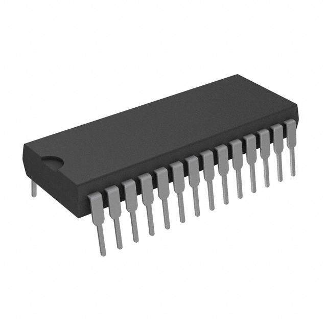
ICGOO在线商城 > 集成电路(IC) > PMIC - 栅极驱动器 > ISL83204AIBZ
- 型号: ISL83204AIBZ
- 制造商: Intersil
- 库位|库存: xxxx|xxxx
- 要求:
| 数量阶梯 | 香港交货 | 国内含税 |
| +xxxx | $xxxx | ¥xxxx |
查看当月历史价格
查看今年历史价格
ISL83204AIBZ产品简介:
ICGOO电子元器件商城为您提供ISL83204AIBZ由Intersil设计生产,在icgoo商城现货销售,并且可以通过原厂、代理商等渠道进行代购。 ISL83204AIBZ价格参考。IntersilISL83204AIBZ封装/规格:PMIC - 栅极驱动器, Half-Bridge Gate Driver IC Inverting, Non-Inverting 20-SOIC。您可以下载ISL83204AIBZ参考资料、Datasheet数据手册功能说明书,资料中有ISL83204AIBZ 详细功能的应用电路图电压和使用方法及教程。
| 参数 | 数值 |
| 产品目录 | 集成电路 (IC) |
| 描述 | IC FET DRVR 60V/2.5A HF 20-SOIC |
| 产品分类 | PMIC - MOSFET,电桥驱动器 - 外部开关 |
| 品牌 | Intersil |
| 数据手册 | |
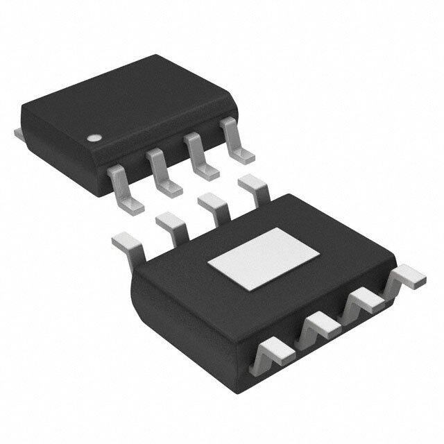
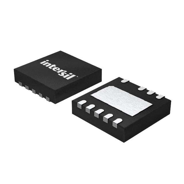
| 产品图片 |
|
| 产品型号 | ISL83204AIBZ |
| rohs | 无铅 / 符合限制有害物质指令(RoHS)规范要求 |
| 产品系列 | - |
| 供应商器件封装 | 20-SOIC W |
| 包装 | 管件 |
| 安装类型 | 表面贴装 |
| 封装/外壳 | 20-SOIC(0.295",7.50mm 宽) |
| 工作温度 | -40°C ~ 85°C |
| 延迟时间 | 70ns |
| 标准包装 | 38 |
| 电压-电源 | 9.5 V ~ 15 V |
| 电流-峰值 | 2.6A |
| 输入类型 | 补充型 |
| 输出数 | 4 |
| 配置 | H 桥 |
| 配置数 | 1 |
| 高压侧电压-最大值(自举) | 75V |





- 商务部:美国ITC正式对集成电路等产品启动337调查
- 曝三星4nm工艺存在良率问题 高通将骁龙8 Gen1或转产台积电
- 太阳诱电将投资9.5亿元在常州建新厂生产MLCC 预计2023年完工
- 英特尔发布欧洲新工厂建设计划 深化IDM 2.0 战略
- 台积电先进制程称霸业界 有大客户加持明年业绩稳了
- 达到5530亿美元!SIA预计今年全球半导体销售额将创下新高
- 英特尔拟将自动驾驶子公司Mobileye上市 估值或超500亿美元
- 三星加码芯片和SET,合并消费电子和移动部门,撤换高东真等 CEO
- 三星电子宣布重大人事变动 还合并消费电子和移动部门
- 海关总署:前11个月进口集成电路产品价值2.52万亿元 增长14.8%


PDF Datasheet 数据手册内容提取
DATASHEET ISL83204A FN6397 60V/2.5A Peak, High Frequency Full Bridge FET Driver Rev.2.00 March 20, 2007 The ISL83204A is a high frequency, medium voltage Full Features Bridge N-Channel FET driver IC, available in 20 lead plastic • Drives N-Channel FET Full Bridge Including High Side SOIC and DIP packages. The ISL83204A includes an input Chop Capability comparator used to facilitate the “hysteresis” and PWM modes of operation. Its HEN (high enable) lead can force • Bootstrap Supply Max Voltage to 75VDC current to freewheel in the bottom two external power • Drives 1000pF Load at 1MHz in Free Air at +50°C with MOSFETs, maintaining the upper power MOSFETs off. Rise and Fall Times of Typically 10ns Since it can switch at frequencies up to 1MHz, the ISL83204A is well suited for driving Voice Coil Motors, • User-Programmable Dead Time switching power amplifiers and power supplies. • Charge-Pump and Bootstrap Maintain Upper Bias Supplies ISL83204A can also drive medium voltage brush motors, and two ISL83204As can be used to drive high performance • DIS (Disable) Pin Pulls Gates Low stepper motors, since the short minimum “on-time” can • Input Logic Thresholds Compatible with 5V to 15V Logic provide fine micro-stepping capability. Levels Short propagation delays of approximately 55ns maximize • Very Low Power Consumption control loop crossover frequencies and dead-times which • Undervoltage Protection can be adjusted to near zero to minimize distortion, resulting in precise control of the driven load. • Pb-Free Plus Anneal Available (RoHS Compliant) Ordering Information Applications TEMP • Medium/Large Voice Coil Motors PART PART RANGE PKG. • Full Bridge Power Supplies NUMBER MARKING (°C) PACKAGE DWG. # ISL83204AIPZ ISL83204AIPZ -40 to +85 20 Ld PDIP E20.3 • Switching Power Amplifiers (Note) (Pb-Free) • Uninterruptible Power Supplies ISL83204AIBZ* ISL83204AIBZ -40 to +85 20 Ld SOIC M20.3 • High Performance Motor Controls (Note) (Pb-Free) • Noise Cancellation Systems *Add “-T” suffix for tape and reel. NOTE: Intersil Pb-free plus anneal products employ special Pb-free • Battery Powered Vehicles material sets; molding compounds/die attach materials and 100% matte tin plate termination finish, which are RoHS compliant and Pinout compatible with both SnPb and Pb-free soldering operations. Intersil Pb-free products are MSL classified at Pb-free peak reflow ISL83204A temperatures that meet or exceed the Pb-free requirements of (20 LD PDIP, 20 LD SOIC) IPC/JEDEC J STD-020. TOP VIEW BHB 1 20 BHO HEN 2 19 BHS DIS 3 18 BLO VSS 4 17 BLS OUT 5 16 VDD IN+ 6 15 VCC IN- 7 14 ALS HDEL 8 13 ALO LDEL 9 12 AHS AHB 10 11 AHO FN6397 Rev.2.00 Page 1 of 15 March 20, 2007
ISL83204A Application Block Diagram 60V 12V BHO BHS LOAD HEN BLO DIS ISL83204A IN+ ALO IN- AHS AHO GND GND Functional Block Diagram (1/2 ISL83204A) AHB HIGH VOLTAGE BUS 60VDC 10 UNDER- CHARGE LEVEL SHIFT DRIVER AHO VOLTAGE PUMP AND LATCH 11 CBS AHS VDD 16 12 HEN 2 TURN-ON DELAY DBS TO VDD (PIN 16) DIS 3 15 VCC OUT 5 DRIVER ALO +12VDC TURN-ON 13 BIAS IN+ 6 + DELAY CBF SUPPLY - ALS IN_ 7 14 HDEL 8 LDEL 9 VSS 4 FN6397 Rev.2.00 Page 2 of 15 March 20, 2007
ISL83204A Typical Application (Hysteresis Mode Switching) 60V 1 BHB BHO 20 12V 2 HEN BHS 19 DIS 3 DIS BLO 18 LOAD 4 VSS A BLS 17 4 5 OUT 20 VDD 16 3 6V 6 IN+ L8 VCC 15 12V S 7 IN- I ALS 14 IN 8 HDEL ALO 13 9 LDEL AHS 12 10 AHB AHO 11 GND - + 6V GND FN6397 Rev.2.00 Page 3 of 15 March 20, 2007
ISL83204A Absolute Maximum Ratings Thermal Information Supply Voltage, VDD and VCC. . . . . . . . . . . . . . . . . . . .-0.3V to 16V Thermal Resistance (Typical, Note 1) JA (°C/W) Logic I/O Voltages . . . . . . . . . . . . . . . . . . . . . . . -0.3V to VDD +0.3V SOIC Package. . . . . . . . . . . . . . . . . . . . . . . . . . . . . 85 Voltage on AHS, BHS . -6.0V (Transient) to 70V (+25°C to +125°C) PDIP Package . . . . . . . . . . . . . . . . . . . . . . . . . . . . . 75 Voltage on AHS, BHS . .-6.0V (Transient) to 70V (-55°C to +125°C) Maximum Power Dissipation at +85°C Voltage on ALS, BLS. . . . . . .-2.0V (Transient) to +2.0V (Transient) SOIC Package. . . . . . . . . . . . . . . . . . . . . . . . . . . . . . . . . .470mW Voltage on AHB, BHB . . . . . . VAHS, BHS -0.3V to VAHS, BHS +VDD PDIP Package . . . . . . . . . . . . . . . . . . . . . . . . . . . . . . . . . .530mW Voltage on ALO, BLO. . . . . . . . . . . . .VALS, BLS -0.3V to VCC +0.3V Storage Temperature Range . . . . . . . . . . . . . . . . . .-65°C to +150°C Voltage on AHO, BHO. . . . . .VAHS, BHS -0.3V to VAHB, BHB +0.3V Operating Max. Junction Temperature. . . . . . . . . . . . . . . . . .+125°C Input Current, HDEL and LDEL. . . . . . . . . . . . . . . . . . -5mA to 0mA Lead Temperature (Soldering 10s) . . . . . . . . . . . . . . . . . . . .+300°C Phase Slew Rate. . . . . . . . . . . . . . . . . . . . . . . . . . . . . . . . . . 20V/ns (For SOIC - Lead Tips Only) All Voltages relative to VSS, unless otherwise specified. Operating Conditions Supply Voltage, VDD and VCC. . . . . . . . . . . . . . . . . . +9.5V to +15V Voltage on ALS, BLS. . . . . . . . . . . . . . . . . . . . . . . . . -1.0V to +1.0V Voltage on AHB, BHB . . . . . . . .VAHS, BHS +5V to VAHS, BHS +15V Voltage on AHs, BHS. . . . . . . . . . . . . . . . . . . . . . . . . . . . . . . . . 60V Input Current, HDEL and LDEL. . . . . . . . . . . . . . . .-500A to -50A Operating Ambient Temperature Range . . . . . . . . . .-40°C to +85°C CAUTION: Stresses above those listed in “Absolute Maximum Ratings” may cause permanent damage to the device. This is a stress only rating and operation of the device at these or any other conditions above those indicated in the operational sections of this specification is not implied. NOTE: 1. JA is measured with the component mounted on a low effective thermal conductivity test board in free air. See Tech Brief TB379 for details. Electrical Specifications VDD = VCC = VAHB = VBHB = 12V, VSS = VALS = VBLS = VAHS = VBHS = 0V, RHDEL = RLDEL = 100k, and TA = +25°C, Unless Otherwise Specified TJ = +25°C TJ = -40°C to +125°C PARAMETERS SYMBOL TEST CONDITIONS MIN TYP MAX MIN MAX UNITS SUPPLY CURRENTS AND CHARGE PUMPS VDD Quiescent Current IDD IN- = 2.5V, Other Inputs = 0V 8 11 14 7 14 mA VDD Operating Current IDDO Outputs switching f = 500kHz, No 8 12 15 8 15 mA Load VCC Quiescent Current ICC IN- = 2.5V, Other Inputs = 0V, - 25 80 - 100 A IALO = IBLO = 0 VCC Operating Current ICCO f = 500kHz, No Load 1 1.25 2.0 0.8 3 mA AHB, BHB Quiescent IAHB, IBHB IN- = 2.5V, Other Inputs = 0V, -50 -25 -11 -60 -10 A Current -Qpump Output IAHO=IBHO= 0, Current VDD = VCC =VAHB = VBHB = 10V AHB, BHB Operating IAHBO, f = 500kHz, No Load 0.62 1.2 1.5 0.5 1.9 mA Current IBHBO AHS, BHS, AHB, BHB IHLK VBHS = VAHS = 60V, - 0.02 1.0 - 10 A Leakage Current VAHB = VBHB = 75V AHB-AHS, BHB-BHS VAHB - VAHS IAHB = IAHB = 0, No Load 11.5 12.6 14.0 10.5 14.5 V Qpump Output Voltage VBHB - VBHS INPUT COMPARATOR PINS: IN+, IN-, OUT Offset Voltage VOS Over Common Mode Voltage -10 0 +10 -15 +15 mV Range Input Bias Current IIB 0 0.5 2 0 4 A Input Offset Current IOS -1 0 +1 -2 +2 A Input Common Mode CMVR 1 - VDD-1.5 1 VDD-1.5 V Voltage Range FN6397 Rev.2.00 Page 4 of 15 March 20, 2007
ISL83204A Electrical Specifications VDD = VCC = VAHB = VBHB = 12V, VSS = VALS = VBLS = VAHS = VBHS = 0V, RHDEL = RLDEL = 100k, and TA = +25°C, Unless Otherwise Specified (Continued) TJ = +25°C TJ = -40°C to +125°C PARAMETERS SYMBOL TEST CONDITIONS MIN TYP MAX MIN MAX UNITS Voltage Gain AVOL - 25 - - - V/mV OUT High Level Output VOH IN+ >IN-, IOH = -250A VDD-0.4 - - VDD-0.5 - V Voltage OUT Low Level Output VOL IN+ <IN-, IOL = +250A - - 0.4 - 0.5 V Voltage Low Level Output Current IOL VOUT = 6V 6.5 14 19 6 20 mA High Level Output Current IOH VOUT = 6V -17 -10 -3 -20 -2.5 mA INPUT PINS: DIS Low Level Input Voltage VIL Full Operating Conditions - - 1.0 - 0.8 V High Level Input Voltage VIH Full Operating Conditions 2.5 - - 2.7 - V Input Voltage Hysteresis - 35 - - - mV Low Level Input Current IIL VIN = 0V, Full Operating Conditions -130 -100 -75 -135 -65 A High Level Input Current IIH VIN = 5V, Full Operating Conditions -1 - +1 -10 +10 A INPUT PINS: HEN Low Level Input Voltage VIL Full Operating Conditions - - 1.0 - 0.8 V High Level Input Voltage VIH Full Operating Conditions 2.5 - - 2.7 - V Input Voltage Hysteresis - 35 - - - mV Low Level Input Current IIL VIN = 0V, Full Operating Conditions -260 -200 -150 -270 -130 A High Level Input Current IIH VIN = 5V, Full Operating Conditions -1 - +1 -10 +10 A TURN-ON DELAY PINS: LDEL AND HDEL LDEL, HDEL Voltage VHDEL,V IHDEL = ILDEL = -100A 4.9 5.1 5.3 4.8 5.4 V GATE DRIVER OUTPUT PINS: ALO, BLO, AHO, AND BHO Low Level Output Voltage VOL IOUT = 100mA 0.7 0.85 1.0 0.5 1.1 V High Level Output Voltage VCC - VOH IOUT = -100mA 0.8 0.95 1.1 0.5 1.2 V Peak Pullup Current IO+ VOUT = 0V 1.7 2.6 3.8 1.4 4.1 A Peak Pulldown Current IO- VOUT = 12V 1.7 2.4 3.3 1.3 3.6 A Under Voltage, Rising UV+ 8.1 8.8 9.4 8.0 9.5 V Threshold Under Voltage, Falling UV- 7.6 8.3 8.9 7.5 9.0 V Threshold Under Voltage, Hysteresis HYS 0.25 0.4 0.65 0.2 0.7 V FN6397 Rev.2.00 Page 5 of 15 March 20, 2007
ISL83204A Switching Specifications VDD = VCC = VAHB = VBHB = 12V, VSS = VALS = VBLS = VAHS = VBHS = 0V, RHDEL = RLDEL = 10k, CL = 1000pF, and TA = +25°C, Unless Otherwise Specified TJ = +25°C TJ = - 40°C to +125°C PARAMETERS SYMBOL TEST CONDITIONS MIN TYP MAX MIN MAX UNITS Lower Turn-off Propagation Delay (IN+/IN- to ALO/BLO) tLPHL - 40 70 - 90 ns Upper Turn-off Propagation Delay (IN+/IN- to AHO/BHO) tHPHL - 50 80 - 110 ns Lower Turn-on Propagation Delay (IN+/IN- to ALO/BLO) tLPLH - 40 70 - 90 ns Upper Turn-on Propagation Delay (IN+/IN- to AHO/BHO) tHPLH - 70 110 - 140 ns Rise Time tR - 10 25 - 35 ns Fall Time tF - 10 25 - 35 ns Turn-on Input Pulse Width tPWIN-ON 50 - - 50 - ns Turn-off Input Pulse Width tPWIN-OFF 40 - - 40 - ns Disable Turn-off Propagation Delay tDISLOW - 45 75 - 95 ns (DIS - Lower Outputs) Disable Turn-off Propagation Delay tDISHIGH - 55 85 - 105 ns (DIS - Upper Outputs) Disable to Lower Turn-on Propagation Delay tDLPLH - 45 70 - 90 ns (DIS - ALO and BLO) Refresh Pulse Width (ALO and BLO) tREF-PW 240 380 500 200 600 ns Disable to Upper Enable (DIS - AHO and BHO) tUEN - 480 630 - 750 ns HEN-AHO, BHO Turn-off, Propagation Delay tHEN-PHL RHDEL = RLDEL = 10k - 40 70 - 90 ns HEN-AHO, BHO Turn-on, Propagation Delay tHEN-PLH RHDEL = RLDEL = 10k - 60 90 - 110 ns TRUTH TABLE INPUT OUTPUT IN+ >IN- HEN U/V DIS ALO AHO BLO BHO X X X 1 0 0 0 0 0 0 0 0 1 0 0 0 1 1 0 0 0 1 1 0 0 1 0 0 1 0 0 1 1 0 0 0 0 0 1 0 X X 1 X 0 0 0 0 FN6397 Rev.2.00 Page 6 of 15 March 20, 2007
ISL83204A Pin Descriptions PIN NUMBER SYMBOL DESCRIPTION 1 BHB B High-side Bootstrap supply. External bootstrap diode and capacitor are required. Connect cathode of bootstrap diode and positive side of bootstrap capacitor to this pin. Internal charge pump supplies 30A out of this pin to maintain bootstrap supply. Internal circuitry clamps the bootstrap supply to approximately 12.8V. 2 HEN High-side Enable input. Logic level input that when low overrides IN+/IN- (Pins 6 and 7) to put AHO and BHO drivers (Pins 11 and 20) in low output state. When HEN is high AHO and BHO are controlled by IN+/IN- inputs. The pin can be driven by signal levels of 0V to 15V (no greater than VDD). 3 DIS DISable input. Logic level input that when taken high sets all four outputs low. DIS high overrides all other inputs. When DIS is taken low the outputs are controlled by the other inputs. The pin can be driven by signal levels of 0V to 15V (no greater than VDD). 4 VSS Chip negative supply, generally will be ground. 5 OUT OUTput of the input control comparator. This output can be used for feedback and hysteresis. 6 IN+ Noninverting input of control comparator. If IN+ is greater than IN- (Pin 7) then ALO and BHO are low level outputs and BLO and AHO are high level outputs. If IN+ is less than IN- then ALO and BHO are high level outputs and BLO and AHO are low level outputs. DIS (Pin 3) high level will override IN+/IN- control for all outputs. HEN (Pin 2) low level will override IN+/IN- control of AHO and BHO. When switching in four quadrant mode, dead time in a half bridge leg is controlled by HDEL and LDEL (Pins 8 and 9). 7 IN- Inverting input of control comparator. See IN+ (Pin 6) description. 8 HDEL High-side turn-on DELay. Connect resistor from this pin to VSS to set timing current that defines the turn-on delay of both high-side drivers. The low-side drivers turn-off with no adjustable delay, so the HDEL resistor guarantees no shoot-through by delaying the turn-on of the high-side drivers. HDEL reference voltage is approximately 5.1V. 9 LDEL Low-side turn-on DELay. Connect resistor from this pin to VSS to set timing current that defines the turn-on delay of both low-side drivers. The high-side drivers turn-off with no adjustable delay, so the LDEL resistor guarantees no shoot-through by delaying the turn-on of the low-side drivers. LDEL reference voltage is approximately 5.1V. 10 AHB A High-side Bootstrap supply. External bootstrap diode and capacitor are required. Connect cathode of bootstrap diode and positive side of bootstrap capacitor to this pin. Internal charge pump supplies 30A out of this pin to maintain bootstrap supply. Internal circuitry clamps the bootstrap supply to approximately 12.8V. 11 AHO A High-side Output. Connect to gate of A High-side power MOSFET. 12 AHS A High-side Source connection. Connect to source of A High-side power MOSFET. Connect negative side of bootstrap capacitor to this pin. 13 ALO A Low-side Output. Connect to gate of A Low-side power MOSFET. 14 ALS A Low-side Source connection. Connect to source of A Low-side power MOSFET. 15 VCC Positive supply to gate drivers. Must be same potential as VDD (Pin 16). Connect to anodes of two bootstrap diodes. 16 VDD Positive supply to lower gate drivers. Must be same potential as VCC (Pin 15). De-couple this pin to VSS (Pin 4). 17 BLS B Low-side Source connection. Connect to source of B Low-side power MOSFET. 18 BLO B Low-side Output. Connect to gate of B Low-side power MOSFET. 19 BHS B High-side Source connection. Connect to source of B High-side power MOSFET. Connect negative side of bootstrap capacitor to this pin. 20 BHO B High-side Output. Connect to gate of B High-side power MOSFET. FN6397 Rev.2.00 Page 7 of 15 March 20, 2007
ISL83204A Timing Diagrams tDT tHPHL U/V = DIS 0 tLPLH HEN 1 IN+ > IN- ALO AHO BLO BHO tLPHL tHPLH tDT (10%t -R 90%)(90% t-F 10%) FIGURE 1. BI-STATE MODE tHEN-PHL tHEN-PLH U/V = DIS 0 HEN IN+ > IN- ALO AHO BLO BHO FIGURE 2. HIGH SIDE CHOP MODE tDLPLH tDIS tREF-PW U/V or DIS HEN IN+ > IN- ALO AHO BLO BHO tUEN FIGURE 3. DISABLE FUNCTION FN6397 Rev.2.00 Page 8 of 15 March 20, 2007
ISL83204A Typical Performance Curves VDD = VCC = VAHB = VBHB = 12V, VSS = VALS = VBLS = VAHS = VBHS = 0V, RHDEL = RLDEL = 100k, and TA = +25°C, Unless Otherwise Specified. 13.0 14 12.5 A) 12 A) m m T ( T ( 12.0 N N E 10 E R R R R U U Y C 8 Y C 11.5 L L P P P P U 6 U 11.0 S S D D D D I I 4 10.5 2 10.0 8 10 12 14 0 200k 400k 600k 800k 1M VDD SUPPLY VOLTAGE (V) SWITCHING FREQUENCY (Hz) FIGURE 4. QUIESCENT IDD SUPPLY CURRENT vs VDD FIGURE 5. IDDO NO-LOAD IDD SUPPLY CURRENT vs SUPPLY VOLTAGE FREQUENCY (Hz) 5 +125°C A) 20 m +75°C T ( A) 4 EN m +25°C CURR 15 RENT ( 3 0°C S R -40°C A U BI C UPPLY 10 UPPLY 2 NG S 5 I SCC 1 TI A O L F 0 0 0 100k 200k300k 400k 500k 600k 700k 800k 900k 1M 0 100k 200k 300k 400k 500k 600k 700k 800k 900k 1M SWITCHING FREQUENCY (Hz) SWITCHING FREQUENCY (Hz) FIGURE 6. SIDE A, B FLOATING SUPPLY BIAS CURRENT vs FIGURE 7. ICCO, NO-LOAD ICC SUPPLY CURRENT vs FREQUENCY (LOAD = 1000pF) FREQUENCY (Hz) TEMPERATURE 2.5 A) RRENT (m 2.0 RENT (A) 1.0 U R C U BIAS 1.5 UT C LY NP PP 1.0 R I U O G S RAT 0.5 N A ATI 0.5 MP O O L C F 0.0 0 200k 400k 6 00k 800k 1M -40 -20 0 20 40 60 80 100 120 SWITCHING FREQUENCY (Hz) JUNCTION TEMPERATURE (°C) FIGURE 8. IAHB, IBHB NO-LOAD FLOATING SUPPLY BIAS FIGURE 9. COMPARATOR INPUT CURRENT IL vs CURRENT vs FREQUENCY TEMPERATURE AT VCM = 5V FN6397 Rev.2.00 Page 9 of 15 March 20, 2007
ISL83204A Typical Performance Curves VDD = VCC = VAHB = VBHB = 12V, VSS = VALS = VBLS = VAHS = VBHS = 0V, RHDEL = RLDEL = 100k, and TA = +25°C, Unless Otherwise Specified. (Continued) -90 -180 A) A) T ( T ( -190 N N E E R -100 R R R U U -200 C C T T U U P P N N L I L I -210 E -110 E V V E E L L W W -220 O O L L -120 -230 -50 -25 0 25 50 75 100 125 -40 -20 0 20 40 60 80 100 120 JUNCTION TEMPERATURE (°C) JUNCTION TEMPERATURE (°C) FIGURE 10. DIS LOW LEVEL INPUT CURRENT IIL vs FIGURE 11. HEN LOW LEVEL INPUT CURRENT IIL vs TEMPERATURE TEMPERATURE V) 80 E ( 15 G A T L 70 VO 14 ns) MP AY ( E PU 13 DEL 60 G N R O G CHA 12 AGATI 50 N P OATI 11 PRO 40 L F D A LO 10 30 O- -40 -20 0 20 40 60 80 100 120 -40 -20 0 20 40 60 80 100 120 N JUNCTION TEMPERATURE (°C) JUNCTION TEMPERATURE (°C) FIGURE 12. AHB - AHS, BHB - BHS NO-LOAD CHARGE PUMP FIGURE 13. UPPER DISABLE TURN-OFF PROPAGATION VOLTAGE vs TEMPERATURE DELAY tDISHIGH vs TEMPERATURE 525 80 ns) 500 ns) 70 AY ( AY ( L L E E 60 D D ON 475 ON GATI GATI 50 A A P P O O R 450 R P P 40 425 30 -50 -25 0 25 50 75 100 125 150 -40 -20 0 20 40 60 80 100 120 JUNCTION TEMPERATURE (°C) JUNCTION TEMPERATURE (°C) FIGURE 14. DISABLE TO UPPER ENABLE tUEN FIGURE 15. LOWER DISABLE TURN-OFF PROPAGATION PROPAGATION DELAY vs TEMPERATURE DELAY tDISLOW vs TEMPERATURE FN6397 Rev.2.00 Page 10 of 15 March 20, 2007
ISL83204A Typical Performance Curves VDD = VCC = VAHB = VBHB = 12V, VSS = VALS = VBLS = VAHS = VBHS = 0V, RHDEL = RLDEL = 100k, and TA = +25°C, Unless Otherwise Specified. (Continued) 450 80 ns) s) 70 DTH ( 425 AY (n 60 WI EL LSE 400 ON D 50 H PU GATI ES PA 40 R O REF 375 PR 30 350 20 -50 -25 0 25 50 75 100 125 150 -40 -20 0 20 40 60 80 100 120 JUNCTION TEMPERATURE (°C) JUNCTION TEMPERATURE (°C) FIGURE 16. tTREF-PW REFRESH PULSE WIDTH vs FIGURE 17. DISABLE TO LOWER ENABLE tDLPLH TEMPERATURE PROPAGATION DELAY vs TEMPERATURE 90 90 ns) 80 ns) 80 Y ( Y ( A A L L DE 70 DE 70 N N O O ATI 60 ATI 60 G G A A P P O O R 50 R 50 P P 40 40 -40 -20 0 20 40 60 80 100 120 -40 -20 0 20 40 60 80 100 120 JUNCTION TEMPERATURE (°C) JUNCTION TEMPERATURE (°C) FIGURE 18. UPPER TURN-OFF PROPAGATION DELAY tHPHL FIGURE 19. UPPER TURN-ON PROPAGATION DELAY tHPLH vs TEMPERATURE vs TEMPERATURE 90 90 ns) 80 ns) 80 Y ( Y ( A A L L DE 70 DE 70 N N O O ATI 60 ATI 60 G G A A P P O O R 50 R 50 P P 40 40 -40 -20 0 20 40 60 80 100 120 -40 -20 0 20 40 60 80 100 120 JUNCTION TEMPERATURE (°C) JUNCTION TEMPERATURE (°C) FIGURE 20. LOWER TURN-OFF PROPAGATION DELAY tLPHL FIGURE 21. LOWER TURN-ON PROPAGATION DELAY tLPLH vs TEMPERATURE vs TEMPERATURE FN6397 Rev.2.00 Page 11 of 15 March 20, 2007
ISL83204A Typical Performance Curves VDD = VCC = VAHB = VBHB = 12V, VSS = VALS = VBLS = VAHS = VBHS = 0V, RHDEL = RLDEL = 100K, and TA = +25°C, Unless Otherwise Specified. 13.5 13.5 s)12.5 12.5 E (n ns) ALL TIM11.5 E TIME ( 11.5 F S E RI RIV10.5 ON 10.5 ATE D URN- G 9.5 T 9.5 8.5 8.5 -40 -20 0 20 40 60 80 100 120 -40 -20 0 20 40 60 80 100 120 JUNCTION TEMPERATURE (°C) JUNCTION TEMPERATURE (°C) FIGURE 22. GATE DRIVE FALL TIME tF vs TEMPERATURE FIGURE 23. GATE DRIVE RISE TIME tR vs TEMPERATURE 6.0 1500 V) 1250 E ( G 5.5 A LT V) 1000 O m T V (H PU 5.0 VO 750 L IN - CC -40°C DE V 500 0°C L L, 4.5 +25°C E D 250 H +75°C +125°C 4.0 0 -40 -20 0 20 40 60 80 100 120 10 12 14 JUNCTION TEMPERATURE (°C) BIAS SUPPLY VOLTAGE (V) FIGURE 24. VLDEL, VHDEL VOLTAGE vs TEMPERATURE FIGURE 25. HIGH LEVEL OUTPUT VOLTAGE, VCC - VOH vs BIAS SUPPLY AND TEMPERATURE AT 100A 1500 3.5 1250 A) 3.0 T ( EN 2.5 1000 RR U mV) K C 2.0 V (OL 750 -40°C VE SIN 1.5 500 RI 0°C D 1.0 E +25°C AT 250 G 0.5 +75°C +125°C 0 0.0 10 12 14 6 7 8 9 10 11 12 13 14 15 16 BIAS SUPPLY VOLTAGE (V) VCC, VDD, VAHG, VBHB (V) FIGURE 26. LOW LEVEL OUTPUT VOLTAGE VOL vs BIAS FIGURE 27. PEAK PULLDOWN CURRENT IO- BIAS SUPPLY SUPPLY AND TEMPERATURE AT 100A VOLTAGE FN6397 Rev.2.00 Page 12 of 15 March 20, 2007
ISL83204A Typical Performance Curves VDD = VCC = VAHB = VBHB = 12V, VSS = VALS = VBLS = VAHS = VBHS = 0V, RHDEL = RLDEL = 100K, and TA = +25°C, Unless Otherwise Specified. (Continued) 3.5 500 A) 3.0 mA) 120000 10,000 T ( T ( EN 2.5 EN 50 3,000 R R UR UR 20 1,000 C 2.0 C K S 10 100 N A E SI 1.5 E BI 5 E DRIV 1.0 OLTAG 12 T V GA 0.5 OW 0.5 L 0.2 0.0 0.1 6 7 8 9 10 11 12 13 14 15 16 1k 2k 5k 10k 20k 50k 100k 200k 500k 1M VCC, VDD, VABH, VBHB (V) SWITCHING FREQUENCY (Hz) FIGURE 28. PEAK PULLUP CURRENT IO+ vs SUPPLY FIGURE 29. LOW VOLTAGE BIAS CURRENT IDD AND ICC VOLTAGE (LESS QUIESCENT COMPONENT) vs FREQUENCY AND GATE LOAD CAPACITANCE 1000 9.0 500 V) UV+ A) (D ENT ( 200 GE, VD 8.8 R A CUR 100 VOLT 8.6 FT LY HI 50 P VEL-S S SUP 8.4 UV- E A L 20 BI 10 8.2 10k 20k 50k 100k 200k 500k 1M 50 25 0 25 50 75 100 125 150 SWITCHING FREQUENCY (Hz) TEMPERATURE (°C) FIGURE 30. HIGH VOLTAGE LEVEL-SHIFT CURRENT vs FIGURE 31. UNDERVOLTAGE LOCKOUT vs TEMPERATURE FREQUENCY AND BUS VOLTAGE 150 120 s) n 90 E ( M TI D- A 60 E D 30 0 10 50 100 150 200 250 HDEL/LDEL RESISTANCE (k) FIGURE 32. MINIMUM DEAD-TIME vs DEL RESISTANCE FN6397 Rev.2.00 Page 13 of 15 March 20, 2007
ISL83204A Dual-In-Line Plastic Packages (PDIP) N E20.3 (JEDEC MS-001-AD ISSUE D) E1 20 LEAD DUAL-IN-LINE PLASTIC PACKAGE INDEX AREA 1 2 3 N/2 INCHES MILLIMETERS -B- SYMBOL MIN MAX MIN MAX NOTES -A- A - 0.210 - 5.33 4 D E A1 0.015 - 0.39 - 4 BASE PLANE A2 -C- A A2 0.115 0.195 2.93 4.95 - SEATING PLANE L CL B 0.014 0.022 0.356 0.558 - B1 0.045 0.070 1.55 1.77 8 D1 D1 A1 eA B1 e eC C C 0.008 0.014 0.204 0.355 - B D 0.980 1.060 24.89 26.9 5 e B 0.010 (0.25) M C A B S D1 0.005 - 0.13 - 5 E 0.300 0.325 7.62 8.25 6 NOTES: E1 0.240 0.280 6.10 7.11 5 1. Controlling Dimensions: INCH. In case of conflict between English e 0.100 BSC 2.54 BSC - and Metric dimensions, the inch dimensions control. eA 0.300 BSC 7.62 BSC 6 2. Dimensioning and tolerancing per ANSI Y14.5M-1982. eB - 0.430 - 10.92 7 3. Symbols are defined in the “MO Series Symbol List” in Section 2.2 of Publication No. 95. L 0.115 0.150 2.93 3.81 4 4. Dimensions A, A1 and L are measured with the package seated in N 20 20 9 JEDEC seating plane gauge GS-3. Rev. 0 12/93 5. D, D1, and E1 dimensions do not include mold flash or protrusions. Mold flash or protrusions shall not exceed 0.010 inch (0.25mm). 6. E and eA are measured with the leads constrained to be perpen- dicular to datum -C- . 7. eB and eC are measured at the lead tips with the leads uncon- strained. eC must be zero or greater. 8. B1 maximum dimensions do not include dambar protrusions. Dam- bar protrusions shall not exceed 0.010 inch (0.25mm). 9. N is the maximum number of terminal positions. 10. Corner leads (1, N, N/2 and N/2 + 1) for E8.3, E16.3, E18.3, E28.3, E42.6 will have a B1 dimension of 0.030 - 0.045 inch (0.76 - 1.14mm). FN6397 Rev.2.00 Page 14 of 15 March 20, 2007
ISL83204A Small Outline Plastic Packages (SOIC) M20.3 (JEDEC MS-013-AC ISSUE C) N 20 LEAD WIDE BODY SMALL OUTLINE PLASTIC PACKAGE IANRDEEAX H 0.25(0.010) M B M INCHES MILLIMETERS E SYMBOL MIN MAX MIN MAX NOTES -B- A 0.0926 0.1043 2.35 2.65 - A1 0.0040 0.0118 0.10 0.30 - 1 2 3 L B 0.014 0.019 0.35 0.49 9 SEATING PLANE C 0.0091 0.0125 0.23 0.32 - -A- D 0.4961 0.5118 12.60 13.00 3 D A h x 45° E 0.2914 0.2992 7.40 7.60 4 -C- e 0.050 BSC 1.27 BSC - H 0.394 0.419 10.00 10.65 - e A1 C h 0.010 0.029 0.25 0.75 5 B 0.10(0.004) L 0.016 0.050 0.40 1.27 6 0.25(0.010) M C A M B S N 20 20 7 0° 8° 0° 8° - NOTES: Rev. 2 6/05 1. Symbols are defined in the “MO Series Symbol List” in Section 2.2 of Publication Number 95. 2. Dimensioning and tolerancing per ANSI Y14.5M-1982. 3. Dimension “D” does not include mold flash, protrusions or gate burrs. Mold flash, protrusion and gate burrs shall not exceed 0.15mm (0.006 inch) per side. 4. Dimension “E” does not include interlead flash or protrusions. Interlead flash and protrusions shall not exceed 0.25mm (0.010 inch) per side. 5. The chamfer on the body is optional. If it is not present, a visual index feature must be located within the crosshatched area. 6. “L” is the length of terminal for soldering to a substrate. 7. “N” is the number of terminal positions. 8. Terminal numbers are shown for reference only. 9. The lead width “B”, as measured 0.36mm (0.014 inch) or greater above the seating plane, shall not exceed a maximum value of 0.61mm (0.024 inch) 10. Controlling dimension: MILLIMETER. Converted inch dimensions are not necessarily exact. © Copyright Intersil Americas LLC 2007. All Rights Reserved. All trademarks and registered trademarks are the property of their respective owners. For additional products, see www.intersil.com/en/products.html Intersil products are manufactured, assembled and tested utilizing ISO9001 quality systems as noted in the quality certifications found at www.intersil.com/en/support/qualandreliability.html Intersil products are sold by description only. Intersil may modify the circuit design and/or specifications of products at any time without notice, provided that such modification does not, in Intersil's sole judgment, affect the form, fit or function of the product. Accordingly, the reader is cautioned to verify that datasheets are current before placing orders. Information furnished by Intersil is believed to be accurate and reliable. However, no responsibility is assumed by Intersil or its subsidiaries for its use; nor for any infringements of patents or other rights of third parties which may result from its use. No license is granted by implication or otherwise under any patent or patent rights of Intersil or its subsidiaries. For information regarding Intersil Corporation and its products, see www.intersil.com FN6397 Rev.2.00 Page 15 of 15 March 20, 2007

 Datasheet下载


