ICGOO在线商城 > 集成电路(IC) > PMIC - 稳压器 - DC DC 切换控制器 > ISL6745AAUZ
 Datasheet下载
- 型号: ISL6745AAUZ
- 制造商: Intersil
- 库位|库存: xxxx|xxxx
- 要求:
| 数量阶梯 | 香港交货 | 国内含税 |
| +xxxx | $xxxx | ¥xxxx |
查看当月历史价格
查看今年历史价格
ISL6745AAUZ产品简介:
ICGOO电子元器件商城为您提供ISL6745AAUZ由Intersil设计生产,在icgoo商城现货销售,并且可以通过原厂、代理商等渠道进行代购。 ISL6745AAUZ价格参考。IntersilISL6745AAUZ封装/规格:PMIC - 稳压器 - DC DC 切换控制器, 全桥,半桥 稳压器 正,可提供隔离 输出 升压/降压 DC-DC 控制器 IC 10-MSOP。您可以下载ISL6745AAUZ参考资料、Datasheet数据手册功能说明书,资料中有ISL6745AAUZ 详细功能的应用电路图电压和使用方法及教程。
| 参数 | 数值 |
| 产品目录 | 集成电路 (IC) |
| Cuk | 无 |
| 描述 | IC REG CTRLR PWM VM 10-MSOP |
| 产品分类 | |
| 品牌 | Intersil |
| 数据手册 | |
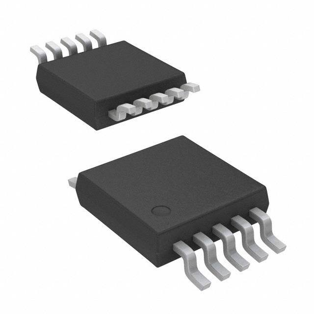
| 产品图片 |
|
| 产品型号 | ISL6745AAUZ |
| PWM类型 | 电压模式 |
| rohs | 无铅 / 符合限制有害物质指令(RoHS)规范要求 |
| 产品系列 | - |
| 倍增器 | 无 |
| 分频器 | 无 |
| 包装 | 管件 |
| 升压 | 无 |
| 占空比 | 100% |
| 反向 | 无 |
| 反激式 | 无 |
| 封装/外壳 | 10-TFSOP,10-MSOP(0.118",3.00mm 宽) |
| 工作温度 | -40°C ~ 105°C |
| 标准包装 | 98 |
| 电压-电源 | 9 V ~ 16 V |
| 输出数 | 2 |
| 降压 | 无 |
| 隔离式 | 无 |
| 频率-最大值 | 2MHz |


- 商务部:美国ITC正式对集成电路等产品启动337调查
- 曝三星4nm工艺存在良率问题 高通将骁龙8 Gen1或转产台积电
- 太阳诱电将投资9.5亿元在常州建新厂生产MLCC 预计2023年完工
- 英特尔发布欧洲新工厂建设计划 深化IDM 2.0 战略
- 台积电先进制程称霸业界 有大客户加持明年业绩稳了
- 达到5530亿美元!SIA预计今年全球半导体销售额将创下新高
- 英特尔拟将自动驾驶子公司Mobileye上市 估值或超500亿美元
- 三星加码芯片和SET,合并消费电子和移动部门,撤换高东真等 CEO
- 三星电子宣布重大人事变动 还合并消费电子和移动部门
- 海关总署:前11个月进口集成电路产品价值2.52万亿元 增长14.8%


PDF Datasheet 数据手册内容提取
DATASHEET ISL6745A FN6703 Improved Bridge Controller with Precision Dead Time Control Rev.2.00 Aug 14, 2017 The ISL6745A is a low-cost, double-ended, voltage-mode Features PWM controller designed for half-bridge and full-bridge •Precision duty cycle and dead time control power supplies and line-regulated bus converters. It provides precise control of switching frequency, adjustable •100µA start-up current soft-start, and overcurrent shutdown. In addition, the •Adjustable delayed overcurrent shutdown and restart ISL6745A allows for accurate adjustment of MOSFET •Adjustable oscillator frequency up to 2MHz non-overlap time (“dead time”) with dead times as low as 35ns, allowing power engineers to optimize the efficiency •1A MOSFET gate drivers of open-loop bus converters. The ISL6745A also includes a •Adjustable soft-start control voltage input for closed-loop PWM and line voltage feed-forward functions. The ISL6745A is identical to the •Internal over-temperature protection ISL6745, but is optimized for higher noise environments. •35ns control to output propagation delay Low start-up and operating currents allow for easy biasing •Small size and minimal external component count in both AC/DC and DC/DC applications. This advanced •Input undervoltage protection BiCMOS design also features adjustable switching frequency up to 1MHz, 1A FET drivers, and very low •Pb-free (RoHS compliant) propagation delays for a fast response to overcurrent faults. Applications The ISL6745A is available in a space-saving 10 Ld MSOP package and is assured to meet rated specifications across a •Half-bridge converters wide -40°C to +105°C temperature range. •Full-bridge converters Related Literature •Line-regulated bus converters •For a full list of related documents, visit our website •AC/DC power supplies •ISL6745A product page •Telecom, datacom, and file server power FN6703 Rev.2.00 Page 1 of 13 Aug 14, 2017
AuFN 1. Overview IS g 167 L67 40 4 , 203R 1.1 Internal Architecture 5A 1e 7v .2 VDDP .0 FL 0 VDD VBIAS VBIAS 5.00V OUTA Q UVLO T + Q OUTB - PWM Toggle Internal VBIAS BG OT Shutdown 130°C - 150°C 70µA GND ON SS VBIAS + SS Clamp - 15µA RTD 2.0V - + SS Charged 3.9V IRTD + - 4.0V VBIAS S Q 160µA R Q OC Latch ON 2.8V - Peak CLK + S Q CT R Q Q Reset 0.8V +- Valley Dominant 50µs Q SS Low + 0.27V Retriggerable - One Shot Fault Latch SS Set Dominant I = 55 x DCHIRTD IDCH SR QQ SR QQ FL ON PSWet MD oLmatinchant VBIAS VBIAS UV - + 4.65V 4.80V BG CS + OC Detect 0.6V - PWM Comparator VBIA CT + S 15µA -- P age VERR 0.8 0.8 SS 1. O 2 Figure1.Internal Architecture ve of 1 rvie 3 w
AuFN 1.2 Typical Application - Telecom DC/DC Converter IS g 167 L67 40 4 , 203R VIN+ 5A 17ev Q1 .2 .0 T1 + VOUT 0 C1 CR1 + C10 36V to 75V CR2 (100V Max.) RETURN T2 L1 Q2 C2 VIN- CR3 CR4 U2 ISL2100A 1VDD LO8 2HB VSS7 C6 3HO LI6 4HS HI5 C9 R11 R1 R6 U1 ISL6745A U3 R10 1SS VDD10 R7 2RTDVDDP9 C8 3VERROUTB8 Q3 4CS OUTA7 5CT GND6 R4 R8 C7 R3 U4 VR1 VR2 R5 TL431 R9 C2 R2 C3 C4 C5 P a Figure2.Typical Application 1 ge . O 3 ve of 1 rvie 3 w
ISL6745A 1. Overview 1.3 Ordering Information Part Number Temp. Range Package Pkg. (Notes1, 2, 3) Part Marking (°C) (RoHS Compliant) Dwg. # ISL6745AAUZ 6745A -40 to +105 10 Ld MSOP M10.118 ISL6745ALEVAL3Z Evaluation Board Notes: 1. Add “-T” suffix for 2.5k unit tape and reel option. Refer to TB347 for details on reel specifications. 2. These Intersil Pb-free plastic packaged products employ special Pb-free material sets, molding compounds/die attach materials, and 100% matte tin plate plus anneal (e3 termination finish, which is RoHS compliant and compatible with both SnPb and Pb-free soldering operations). Intersil Pb-free products are MSL classified at Pb-free peak reflow temperatures that meet or exceed the Pb-free requirements of IPC/JEDEC J STD-020. 3. For Moisture Sensitivity Level (MSL), see the product information page for ISL6745A. For more information on MSL, refer to TB363. 1.4 Pin Configuration ISL6745A (10 Ld MSOP) Top View SS 1 10 VDD RTD 2 9 VDDP VERR 3 8 OUTB CS 4 7 OUTA CT 5 6 GND FN6703 Rev.2.00 Page 4 of 13 Aug 14, 2017
ISL6745A 1. Overview 1.5 Pin Descriptions Pin Pin Name Number Description SS 1 Connect the soft-start timing capacitor between this pin and GND to control the duration of soft-start. The value of the capacitor determines the rate of increase of the duty cycle during start-up, controls the overcurrent shutdown delay, and the overcurrent and short-circuit hiccup restart period. RTD 2 Oscillator timing capacitor discharge current control pin. A resistor is connected between this pin and GND. The current flowing through the resistor determines the magnitude of the discharge current. The discharge current is nominally 55x this current. The PWM dead time is determined by the timing capacitor discharge duration. VERR 3 Inverting input of the PWM comparator. The error voltage is applied to this pin to control the duty cycle. Increasing the signal level increases the duty cycle. The node may be driven with an external error amplifier or an optocoupler. CS 4 Input to the overcurrent protection comparator. The overcurrent comparator threshold is set at 0.600V nominal. The CS pin is shorted to GND at the end of each switching cycle. Depending on the current sensing source impedance, a series input resistor may be required due to the delay between the internal clock and the external power switch. Exceeding the overcurrent threshold will start a delayed shutdown sequence. When an overcurrent condition is detected, the soft-start charge current source is disabled. The soft-start capacitor begins discharging through a 15µA current source, and if it discharges to less than 3.9V (Sustained Overcurrent Threshold), a shutdown condition occurs and the OUTA and OUTB outputs are forced low. When the soft-start voltage reaches 0.27V (Reset Threshold) a soft-start cycle begins. If the overcurrent condition ceases, and then an additional 50µs period elapses before the shutdown threshold is reached, no shutdown occurs. The SS charging current is re-enabled and the soft-start voltage is allowed to recover. CT 5 The oscillator timing capacitor is connected between this pin and GND. GND 6 Reference and power ground for all functions on this device. Due to high peak currents and high frequency operation, a low impedance layout is necessary. Ground planes and short traces are highly recommended. OUTA 7 Alternate half cycle output stages. Each output is capable of 1A peak currents for driving power MOSFETs or MOSFET drivers. Each output provides very low impedance to overshoot and undershoot. OUTB 8 VDDP 9 VDDP is the separate collector supply to the gate drive. Having a separate VDDP pin helps isolate the analog circuitry from the high power gate drive noise. VDD 10 VDD is the power connection for the IC. To optimize noise immunity, bypass VDD to GND with a ceramic capacitor as close to the VDD and GND pins as possible. The total supply current, IDD, will be dependent on the load applied to outputs OUTA and OUTB. Total IDD current is the sum of the quiescent current and the average output current. Knowing the operating frequency, fSW, and the output loading capacitance charge, Q, per output, the average output current can be calculated from (EQ.1): I = 2Qf A (EQ.1) OUT SW FN6703 Rev.2.00 Page 5 of 13 Aug 14, 2017
ISL6745A 2. Specifications 2. Specifications 2.1 Absolute Maximum Ratings Parameter Minimum Maximum Unit Supply Voltage, VDD -0.3 +20.0 V OUTA, OUTB -0.3 VDD V Signal Pins -0.3 5 V Peak GATE Current 1 A CAUTION: Do not operate at or near the maximum ratings listed for extended periods of time. Exposure to such conditions may adversely impact product reliability and result in failures not covered by warranty. 2.2 Thermal Information Thermal Resistance (Typical) JA (°C/W) 10 Ld MSOP Package (Note4) 155 Notes: 4. JA is measured with the component mounted on a high-effective thermal conductivity test board in free air. Refer to TB379. Parameter Minimum Maximum Unit Maximum Junction Temperature -55 +150 °C Maximum Storage Temperature Range -65 +150 °C Pb-Free Reflow Profile refer to TB493 2.3 Recommended Operating Conditions Parameter Minimum Maximum Unit Temperature Range -40 +105 °C Supply Voltage Range (Typical) 9 16 V 2.4 Electrical Specifications Recommended operating conditions unless otherwise noted. Refer to Figure1 on page2 and Figure2 on page3. 9V < VDD < 16V, RTD= 51.1kΩ, CT = 470pF, TA = -40°C to +105°C, typical values are at TA = +25°C. Min Max Parameter Test Conditions (Note5) Typ (Note5) Unit Supply Voltage Start-Up Current, IDD VDD < START Threshold - - 175 µA Operating Current, IDD COUTA,B = 1nF - 5 8.5 mA UVLO START Threshold 5.9 6.3 6.6 V UVLO STOP Threshold 5.3 5.7 6.3 V Hysteresis - 0.6 - V Current Sense Current Limit Threshold 0.55 0.6 0.65 V CS to OUT Delay - 35 - ns CS Sink Current 8 10 - mA FN6703 Rev.2.00 Page 6 of 13 Aug 14, 2017
ISL6745A 2. Specifications Recommended operating conditions unless otherwise noted. Refer to Figure1 on page2 and Figure2 on page3. 9V < VDD < 16V, RTD= 51.1kΩ, CT = 470pF, TA = -40°C to +105°C, typical values are at TA = +25°C. (Continued) Min Max Parameter Test Conditions (Note5) Typ (Note5) Unit Input Bias Current -1 - 1 µA Pulse Width Modulator Minimum Duty Cycle VERROR < CT Offset - - 0 % Maximum Duty Cycle CT = 470pF, RTD = 51.1kΩ - 94 - % CT = 470pF, RTD = 1.1kΩ - 99 - % VERR to PWM Comparator Input Gain - 0.8 - V/V CT to PWM Comparator Input Gain - 1 - V/V SS to PWM Comparator Input Gain - 0.8 - V/V Oscillator Charge Current TA = +25°C 143 156 170 µA RTD Voltage 1.925 2 2.075 V Discharge Current Gain 45 - 65 µA/µA CT Valley Voltage 0.75 0.8 0.85 V CT Peak Voltage 2.70 2.80 2.90 V Soft-Start Net Charging Current 45 - 68 µA SS Clamp Voltage 3.8 4.0 4.2 V Overcurrent Shutdown Threshold Voltage - 3.9 - V Overcurrent Discharge Current 12 15 23 µA Reset Threshold Voltage 0.25 0.27 0.31 V Output High-Level Output Voltage (VOH) VDD - VOUTA or VOUTB, IOUT=-100mA - 0.5 2.0 V Low-Level Output Voltage (VOL) IOUT = 100mA - 0.5 1.0 V Rise Time CGATE = 1nF, VDD = 12V - 17 60 ns Fall Time CGATE = 1nF, VDD = 12V - 20 60 ns Thermal Protection Thermal Shutdown - 145 - °C Thermal Shutdown Clear - 130 - °C Hysteresis, Internal Protection - 15 - °C Notes: 5. Parameters with MIN and/or MAX limits are 100% tested at +25°C, unless otherwise specified. Temperature limits established by characterization and are not production tested. 6. All voltages are to be measured with respect to GND, unless otherwise specified. FN6703 Rev.2.00 Page 7 of 13 Aug 14, 2017
ISL6745A 3. Typical Performance Curves 3. Typical Performance Curves 65 1-104 60 ain CT = 1000pF Current G 55 e (ns) 1-103 CCTT == 648700ppFF ge Tim CT = 270pF ar 50 d h a Disc De 100 CT = 100pF T C 45 40 0.01 0.02 0.03 0.04 0.05 0.06 0.07 0.08 0.09 0.10 10 10 20 30 40 50 60 70 80 90 100 RTD Current (mA) RTD (kΩ) Figure3.Oscillator CT Discharge Current Gain Figure4.Dead Time vs Capacitance 600 1.03 1.02 500 nt kHz) urre 1.01 ncy ( 400 ng C 1.00 e gi equ 300 har 0.99 or Fr ed C 0.98 cillat 200 maliz 0.97 Os or N 100 0.96 0 0.95 -40 -25 -10 5 20 35 50 65 80 95 110 100 200 300 400 500 600 700 800 900 1k CT (pF) Temperature (°C) Figure5.Capacitance vs Oscillator Frequency Figure6.Charge Current vs Temperature (RTD=49.9kΩ) 1.07 1.06 1.05 e g 1.04 a olt V 1.03 d e aliz 1.02 m or 1.01 N 1.00 0.99 0.98 0 10 20 30 40 50 60 70 80 90 100 RTD (kΩ) Figure7.Timing Capacitor Voltage vs RTD FN6703 Rev.2.00 Page 8 of 13 Aug 14, 2017
ISL6745A 4. Functional Description 4. Functional Description 4.2 Oscillator The ISL6745A has an oscillator with a frequency range 4.1 Features to 2MHz, programmable using a resistor RTD and capacitor C . T The ISL6745A PWM is an excellent choice for low cost bridge topologies for applications requiring accurate The switching period may be considered to be the sum frequency and dead time control. Among its many of the timing capacitor charge and discharge durations. features are 1A FET drivers, adjustable soft-start, The charge duration is determined by CT and the overcurrent protection, and internal thermal protection, internal current source (assumed to be 160µA in the allowing a highly flexible design with minimal external formula). The discharge duration is determined by RTD components. and CT. 4 T 1.2510 C s (EQ.2) C T 1 T -----------------------------------------------------------------------------R C s (EQ.3) D CTDischargeCurrentGain TD T 1 T = T +T = ---------------- s (EQ.4) OSC C D F OSC where T and T are the approximate charge and timing capacitor. Additionally, if very low charge and C D discharge times, respectively, T is the oscillator free discharge currents are used, there will be an increased OSC running period, and F is the oscillator frequency. error due to the input impedance at the C pin. OSC T One output switching cycle requires two oscillator The above formulae help with the estimation of the cycles. The actual times will be slightly longer than frequency. Practically, effects like stray capacitances that calculated due to internal propagation delays of affect the overall C capacitance, variation in R T TD approximately 5ns/transition. This delay adds directly to voltage and charge current over-temperature, etc. exist, the switching duration, and also causes overshoot of the and are best evaluated in-circuit. (EQ.2) follows from timing capacitor peak and valley voltage thresholds, the basic capacitor current equation. effectively increasing the peak-to-peak voltage on the dV i = C dt In this case, with variation in dV with R (Figure7 on accurate tool to estimate the operating frequency more TD page8), and in charge current (Figure6 on page8), accurately. results from (EQ.2) would differ from the calculated The maximum duty cycle, D, and dead time, DT, can be frequency. The typical performance curves may be used calculated from: as a tool along with the previous equations as a more D = T T (EQ.5) C OSC DT = 1–DT s (EQ.6) OSC FN6703 Rev.2.00 Page 9 of 13 Aug 14, 2017
ISL6745A 4. Functional Description 4.3 Soft-Start Operation 4.7 Ground Plane Requirements The ISL6745A features a soft-start using an external Careful layout is essential for satisfactory operation of capacitor in conjunction with an internal current source. the device. A good ground plane must be employed. Soft-start reduces stresses and surge currents during V should be bypassed directly to GND with good DD start-up. high-frequency capacitance. The oscillator capacitor signal, C , is compared to the T soft-start voltage, SS, in the SS comparator which drives the PWM latch. While the SS voltage is less than 3.5V, duty cycle is limited. The output pulse width increases as the soft-start capacitor voltage increases up to 3.5V. This has the effect of increasing the duty cycle from zero to the maximum pulse width during the soft-start period. When the soft-start voltage exceeds 3.5V, soft-start is completed. Soft-start occurs during start-up and after recovery from an overcurrent shutdown. The soft-start voltage is clamped to 4V. Please note the capacitance of the soft-start capacitor, C . If C ≥ 0.1µF, the user will need to add a resistor SS SS in series with the capacitor, 100Ω/µF (100Ω at least; 1k at most). 4.4 Gate Drive The ISL6745A is capable of sourcing and sinking 1A peak current, and may also be used in conjunction with a MOSFET driver such as the ISL6700 for level shifting. To limit the peak current through the IC, an external resistor may be placed between the totem-pole output of the IC (OUTA or OUTB pin) and the gate of the MOSFET. This small series resistor also damps any oscillations caused by the resonant tank of the parasitic inductances in the traces of the board and the FET’s input capacitance. 4.5 Overcurrent Operation Overcurrent delayed shutdown is enabled once the soft- start cycle is complete. If an overcurrent condition is detected, the soft-start charging current source is disabled and the soft-start capacitor is allowed to discharge through a 15µA source. At the same time a 50µs retriggerable one-shot timer is activated. It remains active for 50µs after the overcurrent condition ceases. If the soft-start capacitor discharges to 3.9V, the output is disabled. This state continues until the soft-start voltage reaches 270mV, at which time a new soft-start cycle is initiated. If the overcurrent condition stops at least 50µs prior to the soft-start voltage reaching 3.9V, the soft-start charging currents revert to normal operation and the soft-start voltage is allowed to recover. 4.6 Thermal Protection An internal temperature sensor protects the device if the junction temperature exceeds +145°C. There is approximately +15°C of hysteresis. FN6703 Rev.2.00 Page 10 of 13 Aug 14, 2017
ISL6745A 5. Revision History 5. Revision History Rev. Date Description 2.00 Aug 14, 2017 Applied new formatting. Added Related Literature section. Updated Ordering information table. Update Absolute Maximum Ratings minimum values for Supply Voltage, OUTA, OUTB, and Signal Pins. Added Notes 3 and 6. Removed old Note 3 on EC table along with references as Note 6 covers this statement. Moved Pin Descriptions to table following Pin Configuration. Updated the Soft-Start Operation section on page 10. Added Revision History and About Intersil sections. Updated POD M10.118 to the latest revision. The updates are as follows: -Updated to new POD template. Added land pattern. FN6703 Rev.2.00 Page 11 of 13 Aug 14, 2017
ISL6745A 6. Package Outline Drawing 6. Package Outline Drawing 10 LEAD MINI SMALL OUTLINE PLASTIC PACKAGE Rev 1, 4/12 M10.118 For the most recent package outline drawing, see M10.118. 5 3.0±0.05 A DETAIL "X" D 10 1.10 MAX SIDE VIEW 2 0.09 - 0.20 4.9±0.15 3.0±0.05 5 PIN# 1 ID 0.95 REF 1 2 0.50 BSC B GAUGE TOP VIEW PLANE 0.25 3°±3° 0.55 ± 0.15 0.85±010 H DETAIL "X" C SEATING PLANE 0.18 - 0.27 0.08MCA-BD 0.10 ± 0.05 0.10C SIDE VIEW 1 (5.80) NOTES: (4.40) (3.00) 1. Dimensions are in millimeters. 2. Dimensioning and tolerancing conform to JEDEC MO-187-BA and AMSEY14.5m-1994. 3. Plastic or metal protrusions of 0.15mm max per side are not included. (0.50) 4. Plastic interlead protrusions of 0.15mm max per side are not included. (0.29) 5. Dimensions are measured at Datum Plane "H". (1.40) 6. Dimensions in ( ) are for reference only. TYPICAL RECOMMENDED LAND PATTERN FN6703 Rev.2.00 Page 12 of 13 Aug 14, 2017
ISL6745A ISL6745A 7. About Intersil 7. About Intersil Intersil Corporation is a leading provider of innovative power management and precision analog solutions. The company's products address some of the largest markets within the industrial and infrastructure, mobile computing, and high-end consumer markets. For the most updated datasheet, application notes, related documentation, and related parts, see the respective product information page found at www.intersil.com. For a listing of definitions and abbreviations of common terms used in our documents, visit: www.intersil.com/glossary. You can report errors or suggestions for improving this datasheet by visiting www.intersil.com/ask. Reliability reports are also available from our website at www.intersil.com/support. © Copyright Intersil Americas LLC 2008-2017. All Rights Reserved. All trademarks and registered trademarks are the property of their respective owners. For additional products, see www.intersil.com/en/products.html Intersil products are manufactured, assembled and tested utilizing ISO9001 quality systems as noted in the quality certifications found at www.intersil.com/en/support/qualandreliability.html Intersil products are sold by description only. Intersil may modify the circuit design and/or specifications of products at any time without notice, provided that such modification does not, in Intersil's sole judgment, affect the form, fit or function of the product. Accordingly, the reader is cautioned to verify that datasheets are current before placing orders. Information furnished by Intersil is believed to be accurate and reliable. However, no responsibility is assumed by Intersil or its subsidiaries for its use; nor for any infringements of patents or other rights of third parties which may result from its use. No license is granted by implication or otherwise under any patent or patent rights of Intersil or its subsidiaries. For information regarding Intersil Corporation and its products, see www.intersil.com FN6703 Rev.2.00 Page 13 of 13 Aug 14, 2017