ICGOO在线商城 > 集成电路(IC) > PMIC - 稳压器 - 专用型 > ISL6561CRZ-T

 Datasheet下载
- 型号: ISL6561CRZ-T
- 制造商: Intersil
- 库位|库存: xxxx|xxxx
- 要求:
| 数量阶梯 | 香港交货 | 国内含税 |
| +xxxx | $xxxx | ¥xxxx |
查看当月历史价格
查看今年历史价格
ISL6561CRZ-T产品简介:
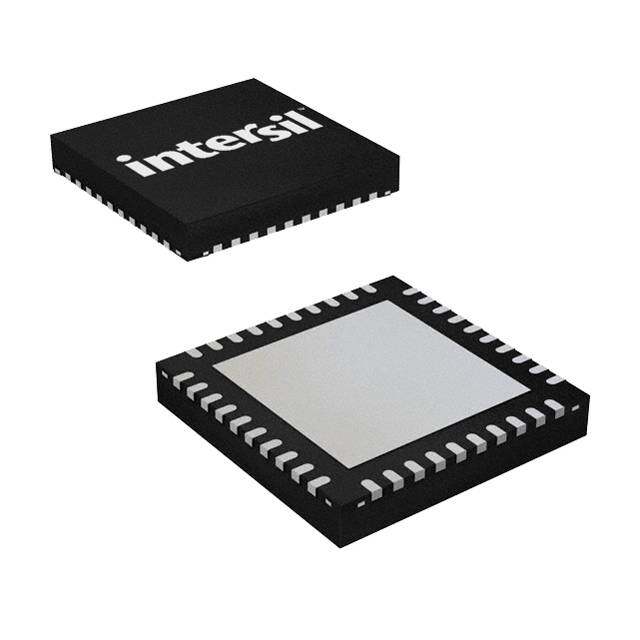
ICGOO电子元器件商城为您提供ISL6561CRZ-T由Intersil设计生产,在icgoo商城现货销售,并且可以通过原厂、代理商等渠道进行代购。 ISL6561CRZ-T价格参考¥23.17-¥23.17。IntersilISL6561CRZ-T封装/规格:PMIC - 稳压器 - 专用型, - Controller, Intel VR10X Voltage Regulator IC 4 Output 40-QFN (6x6)。您可以下载ISL6561CRZ-T参考资料、Datasheet数据手册功能说明书,资料中有ISL6561CRZ-T 详细功能的应用电路图电压和使用方法及教程。
ISL6561CRZ-T 是由 Renesas Electronics America Inc. 生产的一款专用型 PMIC(电源管理集成电路),属于稳压器系列。该型号主要应用于需要高效、稳定电源管理的场景,以下是其典型应用场景:

 1. 笔记本电脑和台式机
   - ISL6561CRZ-T 提供多相电压调节功能,适合为高性能处理器(如 CPU 和 GPU)供电。它能够满足现代计算设备对高电流和低电压的需求,确保系统在高负载下仍能稳定运行。

 2. 服务器和数据中心
   - 在服务器和数据中心中,该芯片可用于为主板上的关键组件(如多核处理器、FPGA 等)提供精确的电压调节。其高效的电源转换能力有助于降低能耗,提高系统的整体效率。

 3. 通信设备
   - 适用于路由器、交换机和其他网络设备,为其中的高性能 ASIC 或 SoC 提供稳定的电源支持。其快速瞬态响应特性可应对通信设备中复杂的动态负载需求。

 4. 嵌入式系统
   - 在工业自动化、医疗设备或物联网设备中,ISL6561CRZ-T 可为微控制器、DSP 或其他核心处理单元提供可靠的电源管理解决方案,确保系统在各种环境条件下正常工作。

 5. 图形卡(GPU)
   - 高性能显卡需要强大的电源支持,ISL6561CRZ-T 的多相输出设计可以为 GPU 提供所需的高电流和低纹波电压,保证图形处理的稳定性。

 6. 存储设备
   - 在 SSD 控制器或 RAID 系统中,该芯片可以为存储设备中的主控芯片和其他关键组件提供高效电源管理,提升数据传输速度和可靠性。

 特性总结
- 支持多相输出,适用于多核处理器或多负载系统。
- 高效电源转换,降低功耗和发热。
- 快速瞬态响应,适应动态负载变化。
- 小型封装设计,节省电路板空间。

综上所述,ISL6561CRZ-T 广泛应用于需要高性能电源管理的各种电子设备中,特别是在计算密集型和高功率需求的场景下表现出色。
| 参数 | 数值 |
| 产品目录 | 集成电路 (IC) |
| 描述 | IC CTLR PWM MULTIPHASE 40-QFN |
| 产品分类 | |
| 品牌 | Intersil |
| 数据手册 | |
| 产品图片 |
|
| 产品型号 | ISL6561CRZ-T |
| PCN过时产品 | |
| rohs | 无铅 / 符合限制有害物质指令(RoHS)规范要求 |
| 产品系列 | - |
| 产品目录页面 | |
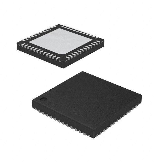
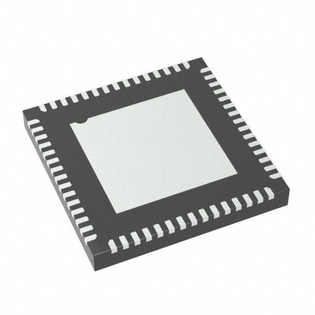
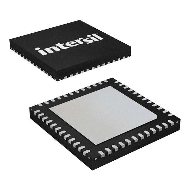
| 供应商器件封装 | 40-QFN(6x6) |
| 其它名称 | ISL6561CRZ-TCT |
| 包装 | 剪切带 (CT) |
| 安装类型 | 表面贴装 |
| 封装/外壳 | 40-VFQFN 裸露焊盘 |
| 工作温度 | 0°C ~ 70°C |
| 应用 | 控制器,Intel VR10X |
| 标准包装 | 1 |
| 电压-输入 | 3 V ~ 12 V |
| 电压-输出 | 0.84 V ~ 1.6 V |
| 输出数 | 4 |


- 商务部:美国ITC正式对集成电路等产品启动337调查
- 曝三星4nm工艺存在良率问题 高通将骁龙8 Gen1或转产台积电
- 太阳诱电将投资9.5亿元在常州建新厂生产MLCC 预计2023年完工
- 英特尔发布欧洲新工厂建设计划 深化IDM 2.0 战略
- 台积电先进制程称霸业界 有大客户加持明年业绩稳了
- 达到5530亿美元!SIA预计今年全球半导体销售额将创下新高
- 英特尔拟将自动驾驶子公司Mobileye上市 估值或超500亿美元
- 三星加码芯片和SET,合并消费电子和移动部门,撤换高东真等 CEO
- 三星电子宣布重大人事变动 还合并消费电子和移动部门
- 海关总署:前11个月进口集成电路产品价值2.52万亿元 增长14.8%


PDF Datasheet 数据手册内容提取
DATASHEET ISL6561 FN9098 Multi-Phase PWM Controller with Precision r or DCR Differential Current Rev 6.00 DS(ON) Sensing for VR10.X Application November 10, 2015 The ISL6561 controls microprocessor core voltage regulation Features by driving up to 4 synchronous-rectified buck channels in • Precision Multi-Phase Core Voltage Regulation parallel. Multi-phase buck converter architecture uses interleaved timing to multiply channel ripple frequency and - Differential Remote Voltage Sensing reduce input and output ripple currents. Lower ripple results in - 0.5% System Accuracy Over Life, Load, Line and fewer components, lower component cost, reduced power Temperature dissipation, and smaller implementation area. - Adjustable Reference-Voltage Offset Microprocessor loads can generate load transients with • Precision rDS(ON) or DCR Current Sensing extremely fast edge rates. The ISL6561 features a high - Integrated Programmable Temperature Compensation bandwidth control loop and ripple frequencies of >4MHz to - Accurate Load-Line Programming provide optimal response to the transients. - Accurate Channel-Current Balancing - Differential Current Sense Today’s microprocessors require a tightly regulated output - Low-Cost, Lossless Current Sensing voltage position versus load current (droop). The ISL6561 senses current by utilizing patented techniques to measure • Internal Shunt Regulator for 5V or 12V Biasing the voltage across the on resistance, rDS(ON), of the lower • Microprocessor Voltage Identification Input MOSFETs or DCR of the output inductor during the lower - Dynamic VID™ technology MOSFET conduction intervals. Current sensing provides the - 6-Bit VID Input needed signals for precision droop, channel-current balancing, and overcurrent protection. - 0.8375V to 1.600V in 12.5mV Steps • Threshold-Sensitive Enable Function for synchronizing The accuracy of the current-sensing method is enhanced by with driver POR the ISL6561’s temperature compensation function. Droop accuracy can be affected by increasing rDS(ON) or DCR with • Overcurrent Protection elevated temperature. The ISL6561 uses an internal • Overvoltage Protection temperature-sensing element to provide programmable - No Additional External Components Needed temperature compensation. Correctly applied, temperature - OVP Pin to drive opitional Crowbar Device compensation can completely nullify the effect of rDS(ON) or DCR temperature sensitivity. • 2, 3, or 4 Phase Operation A unity gain, differential amplifier is provided for remote • Greater Than 1MHz Operation (> 4MHz Ripple) voltage sensing. Any potential difference between remote • Pb-free Available (RoHS Compliant) and local grounds can be completely eliminated using the • QFN Package Option remote-sense amplifier. Eliminating ground differences improves regulation and protection accuracy. The threshold- - QFN Compliant to JEDEC PUB95 MO-220 QFN - Quad Flat No Leads - Product Outline sensitive enable input is available to accurately coordinate the start up of the ISL6561 with any other voltage rail. - QFN Near Chip Scale Package Footprint; Improves PCB Efficiency, Thinner in Profile Dynamic-VID™ technology allows seamless on-the-fly VID changes. The offset pin allows accurate voltage offset settings that are independent of VID setting. The ISL6561 uses 5V bias and has a built-in shunt regulator to allow 12V bias using only a small external limiting resistor. FN9098 Rev 6.00 Page 1 of 27 November 10, 2015
ISL6561 Ordering Information TEMP. PACKAGE PKG. PART NUMBER (°C) (RoHS Compliant) DWG # ISL6561IRZ (Note) -40 to 85 40 Ld 6x6 QFN (Pb-free) L40.6x6 ISL6561IRZ-T (Note) 40 Ld 6x6 QFN Tape and Reel L40.6x6 (Pb-free) NOTE: Intersil Pb-free products employ special Pb-free material sets; molding compounds/die attach materials and 100% matte tin plate termination finish, which are RoHS compliant and compatible with both SnPb and Pb-free soldering operations. Intersil Pb-free products are MSL classified at Pb-free peak reflow temperatures that meet or exceed the Pb-free requirements of IPC/JEDEC J STD-020. Pinout ISL6561 (40-PIN QFN) TOP VIEW D ND GOO VP ND S ND NLL N CC WM4 G P O G F G E E V P 40 39 38 37 36 35 34 33 32 31 VID4 1 30 ISEN4+ VID3 2 29 ISEN4- VID2 3 28 ISEN2- VID1 4 27 ISEN2+ VID0 5 26 PWM2 VID12.5 6 25 PWM1 GND 7 24 ISEN1+ OFS 8 23 ISEN1- TCOMP 9 22 ISEN3- DAC 10 21 ISEN3+ 11 12 13 14 15 16 17 18 19 20 F D B P P F N D D 3 E N F O M F E N N M R G O O DI S G G W R C V V R P D I FN9098 Rev 6.00 Page 2 of 27 November 10, 2015
ISL6561 ISL6561CR Block Diagram VDIFF PGOOD OVP VCC ENLL RGND S OVP R POWER-ON 1.24V x1 LATCH VSEN RESET (POR) EN Q THREE-STATE OVP SOFT START CLOCK AND AND SAWTOOTH FS FAULT LOGIC GENERATOR +200mV PWM1 PWM OFS OFFSET PWM PWM2 REF PWM3 PWM DAC VID4 VID3 PWM4 PWM VID2 DYNAMIC VID VID1 D/A E/A VID0 CHANNEL CHANNEL VID12.5 CURRENT DETECT BALANCE COMP ISEN1+ FB I_TRIP ISEN1- OC IDROOP SAM&PLE CHANNEL ISEN2+ HOLD CURRENT ISEN2- TCOMP SENSE I_TOT ISEN3+ T ISEN3- ISEN4+ ISEN4- GND FN9098 Rev 6.00 Page 3 of 27 November 10, 2015
ISL6561 Typical Application - 4-Phase Buck Converter with Rds,on Sensing and External NTC +12V VCC VIN BOOT UGATE PVCC PHASE HIP6601B PWM DRIVER LGATE NTC +5V GND THERMISTOR FB COMP REF +12V IDROOP VDIFF DAC VCC BOOT VIN VSEN VCC RGND VIDPGOOD ENLL UGATE PGOOD ISL6561 PVCC PHASE OVP VID4 ISEN1+ HIP6601B PWM ISEN1- DRIVER VID3 LGATE PWM1 GND VID2 PWM2 ISEN2+ VID1 ISEN2- VID0 PWM3 +12V VIN VID12.5 ISEN3+ P ISEN3- VCC LOAD OFS PWM4 BOOT FS ISEN4+ UGATE ISEN4- PVCC PHASE RTTCOMPGND EN HIP6601B PWM DRIVER LGATE GND +12V +12V VCC VIN BOOT UGATE PVCC PHASE HIP6601B PWM DRIVER LGATE GND FN9098 Rev 6.00 Page 4 of 27 November 10, 2015
ISL6561 Typical Application - 4-Phase Buck Converter with r Sensing and Internal PTC DS(ON) +12V VCC VIN BOOT UGATE PVCC PHASE HIP6601B PWM DRIVER LGATE GND +5V FB COMP REF +12V IDROOP VDIFF DAC VCC BOOT VIN VSEN VCC RGND VIDPGOOD ENLL UGATE PGOOD ISL6561 PVCC PHASE OVP VID4 ISEN1+ HIP6601B PWM ISEN1- DRIVER VID3 LGATE PWM1 GND VID2 PWM2 ISEN2+ VID1 ISEN2- VID0 PWM3 +12V VIN VID12.5 ISEN3+ P ISEN3- VCC LOAD OFS PWM4 BOOT FS ISEN4+ UGATE ISEN4- PVCC PHASE RT TCOMP GND EN HIP6601B PWM DRIVER LGATE +12V GND +12V VCC VIN BOOT UGATE PVCC PHASE HIP6601B PWM DRIVER LGATE GND FN9098 Rev 6.00 Page 5 of 27 November 10, 2015
ISL6561 Typical Application - 4-Phase Buck Converter with DCR Sensing and External NTC +12V VCC VIN BOOT UGATE PVCC PHASE HIP6601B PWM DRIVER LGATE NTC +5V GND THERMISTOR FB COMP REF +12V IDROOP VDIFF DAC VCC BOOT VIN VSEN VCC RGND VIDPGOOD ENLL UGATE PGOOD ISL6561 PVCC PHASE OVP ISEN1+ HIP6601B VID4 PWM ISEN1- DRIVER VID3 LGATE PWM1 GND VID2 PWM2 VID1 ISEN2+ ISEN2- VID0 PWM3 +12V VIN VID12.5 ISEN3+ P ISEN3- VCC LOAD OFS PWM4 BOOT FS ISEN4+ UGATE ISEN4- PVCC PHASE RT TCOMP GND EN HIP6601B PWM DRIVER LGATE +12V GND +12V VCC VIN BOOT UGATE PVCC PHASE HIP6601B PWM DRIVER LGATE GND FN9098 Rev 6.00 Page 6 of 27 November 10, 2015
ISL6561 Typical Application - 4-Phase Buck Converter with DCR Sensing and Internal PTC +12V VCC VIN BOOT UGATE PVCC PHASE HIP6601B PWM DRIVER LGATE GND +5V FB COMP REF +12V IDROOP VDIFF DAC VCC BOOT VIN VSEN VCC RGND VIDPGOOD ENLL UGATE PGOOD ISL6561 PVCC PHASE OVP VID4 ISEN1+ HIP6601B PWM ISEN1- DRIVER VID3 LGATE PWM1 GND VID2 PWM2 ISEN2+ VID1 ISEN2- VID0 PWM3 +12V VIN VID12.5 ISEN3+ P ISEN3- VCC LOAD OFS PWM4 BOOT FS ISEN4+ UGATE ISEN4- PVCC PHASE RT TCOMP GND EN HIP6601B PWM DRIVER +12V LGATE GND +12V VCC VIN BOOT UGATE PVCC PHASE HIP6601B PWM DRIVER LGATE GND FN9098 Rev 6.00 Page 7 of 27 November 10, 2015
ISL6561 Absolute Maximum Ratings Thermal Information Supply Voltage, VCC . . . . . . . . . . . . . . . . . . . . . . . . . . . . . . . . . +7V Thermal Resistance JA (°C/W) JC (°C/W) Input, Output, or I/O Voltage (except OVP)GND -0.3V to VCC + 0.3V QFN Package (Notes 1, 2). . . . . . . . 32 3.5 OVP Voltage. . . . . . . . . . . . . . . . . . . . . . . . . . . . . . . . . . . . . . . +15V Maximum Junction Temperature. . . . . . . . . . . . . . . . . . . . . . .150°C SD (Human body model. . . . . . . . . . . . . . . . . . . . . . . . . . . . . . >4kV Maximum Storage Temperature Range. . . . . . . . . . .-65°C to 150°C ESD (Machine model . . . . . . . . . . . . . . . . . . . . . . . . . . . . . . . >300V Maximum Lead Temperature (Soldering 10s) . . . . . . . . . . . . .300°C ESD (Charged device model . . . . . . . . . . . . . . . . . . . . . . . . . . >2kV (SOIC - Lead Tips Only) Operating Conditions Supply Voltage, VCC (5V bias mode, Note 3) . . . . . . . . . . +5V ±5% Ambient Temperature (ISL6561CR, ISL6561CRZ). . . . .0°C to 70°C Ambient Temperature (ISL6561IR, ISL6561IRZ) . . . . -40°C to 85°C CAUTION: Stress above those listed in “Absolute Maximum Ratings” may cause permanent damage to the device. This is a stress only rating and operation of the device at these or any other conditions above those indicated in the operational section of this specification is not implied. NOTES: 1. JA is measured in free air with the component mounted on a high effective thermal conductivity test board with “direct attach” features. See Tech Brief TB379 2. For JC, the “case temp” location is the center of the exposed metal pad on the package underside. Electrical Specifications Operating Conditions: VCC = 5V or ICC < 25mA (Note 3). Unless Otherwise Specified PARAMETER TEST CONDITIONS MIN TYP MAX UNITS VCC SUPPLY CURRENT Nominal Supply VCC = 5VDC; EN = 5VDC; RT = 100 k - 14 18 mA ISEN1 = ISEN2 = ISEN3 = ISEN4 = -70A Shutdown Supply VCC = 5VDC; EN = 0VDC; RT = 100 k - 10 14 mA SHUNT REGULATOR VCC Voltage VCC tied to 12VDC thru 300 resistor, , RT = 100k 5.6 5.9 6.3 V VCC Sink Current VCC tied to 12VDC thru 300 resistor, RT = 100k - - 25 mA POWER-ON RESET AND ENABLE POR Threshold VCC Rising 4.15 4.31 4.51 V VCC Falling 3.68 3.82 4.05 V ENABLE Threshold EN Rising 1.22 1.24 1.26 V Hysteresis 100 mV Fault Reset 1.10 1.14 1.18 V ENLL Input Logic Low Level - - 0.4 V ENLL input Logic High Level 0.8 - - V ENLL Leakage Current ENLL=5V 1 A REFERENCE VOLTAGE AND DAC System Accuracy (VID = 1.2V-1.6V) (0°C to (Note 4) -0.5 - 0.5 %VID 85°C) System Accuracy (VID = 1.2V-1.6V) (- (Note 4) -0.8 - 0.8 %VID 40°C) System Accuracy (VID = 0.8375V- (Note 4) -0.8 - 0.8 %VID 1.1875V) (0°C to 85°C) System Accuracy (VID = 0.8375V- (Note 4) -1.1 - 1.1 %VID 1.1875V) (-40°C) VID Pull Up -65 -50 -35 A VID Input Low Level - - 0.4 V VID Input High Level 0.8 - - V DAC Source/Sink Current VID = 010100 -200 - 200 A REF Source/Sink Current -50 - 50 A FN9098 Rev 6.00 Page 8 of 27 November 10, 2015
ISL6561 Electrical Specifications Operating Conditions: VCC = 5V or ICC < 25mA (Note 3). Unless Otherwise Specified (Continued) PARAMETER TEST CONDITIONS MIN TYP MAX UNITS PIN-ADJUSTABLE OFFSET Voltage at OFS pin Offset resistor connected to ground 485 500 515 mV VCC = 5.00V, offset resistor connected to VCC 2.91 3.00 3.09 V OSCILLATOR Accuracy RT = 100 k -10 - 10 % Adjustment Range 0.08 - 1.5 MHz Sawtooth Amplitude - 1.5 - V Max Duty Cycle - 66.7 - % ERROR AMPLIFIER Open-Loop Gain RL = 10k to ground - 80 - dB Open-Loop Bandwidth CL = 100pF, RL = 10k to ground - 18 - MHz Slew Rate CL = 100pF 4.4 6.0 7.5 V/s Maximum Output Voltage 4.0 4.3 - V Output High Voltage @ 2mA 3.7 - - V Output Low Voltage @ 2mA - - 1.40 V REMOTE-SENSE AMPLIFIER Bandwidth - 20 - MHz Output High Current VSEN - RGND = 2.5V -500 - 500 A Output High Current VSEN - RGND = 0.6 -500 - 500 A PWM OUTPUT PWM Output Voltage LOW Threshold Iload = ±500A - - 0.3 V PWM Output Voltage HIGH Threshold Iload = ±500A 4.3 - - V TEMPERATURE COMPENSATION Temperature Compensation Current @ 10 15 20 A 40°C and Tcomp = 0.5V Temperature Compensation - 1 - 1A/V/ Transconductance °C SENSE CURRENT Sensed Current Tolerance (0°C to 85°C) ISEN1 = ISEN2 = ISEN3 = ISEN4 = 80A 74 81 91 A Sensed Current Tolerance (-40°C) ISEN1 = ISEN2 = ISEN3 = ISEN4 = 80A 74 81 92 A Overcurrent Trip Level (0°C to 85°C) 98 110 122 A Overcurrent Trip Level (-40°C) 98 110 127 A POWER GOOD AND PROTECTION MONITORS PGOOD Low Voltage IPGOOD = 4mA - - 0.4 V Under-Voltage Offset From VID (0°C to VSEN Falling 72 74 76 %VID 85°C) Under-Voltage Offset From VID (-40°C) VSEN Falling 71 74 82 %VID Overvoltage Threshold Voltage above VID, After Soft Start (Note 5) 180 200 220 mV Before Enable 1.63 V VCC < POR Threshold 1.67 1.80 1.87 V Overvoltage Reset Voltage VCC POR Threshold, VSEN Falling - 0.6 - V VCC < POR Threshold - 1.5 - V OVP Drive Voltage IOVP = -100mA, VCC = 5V - 1.9 - V Minimum VCC for OVP 1.4 - - V NOTES: 3. When using the internal shunt regulator, VCC is clamped to 6.02V (max). Current must be limited to 25mA or less. 4. These parts are designed and adjusted for accuracy with all errors in the voltage loop included. 5. During soft start, VDAC rises from 0 to VID. The overvoltage trip level is the higher of 1.7V and VDAC + 0.2V. FN9098 Rev 6.00 Page 9 of 27 November 10, 2015
ISL6561 Functional Pin Description 1k, 1% resistor is used between DAC and REF to generate a precise offset voltage. This voltage is proportional to the VCC - Supplies all the power necessary to operate the chip. offset current determined by the offset resistor from OFS to The controller starts to operate when the voltage on this pin ground or VCC. A capacitor is used between REF and exceeds the rising POR threshold and shuts down when the ground to smooth the voltage transition during Dynamic voltage on this pin drops below the falling POR threshold. VID™ operations. Connect this pin directly to a +5V supply or through a series 300 resistor to a +12V supply. PWM1, PWM2, PWM3, PWM4 - Pulse-width modulation outputs. Connect these pins to the PWM input pins of the GND - Bias and reference ground for the IC. Intersil driver IC. The number of active channels is EN - This pin is a threshold-sensitive enable input for the determined by the state of PWM3 and PWM4. Tie PWM3 to controller. Connecting the 12V supply to EN through an VCC to configure for 2-phase operation. Tie PWM4 to VCC appropriate resistor divider provides a means to synchronize to configure for 3-phase operation. power-up of the controller and the MOSFET driver ICs. ISEN1+, ISEN1-; ISEN2+, ISEN2-; ISEN3+, ISEN3-; When EN is driven above 1.24V, the ISL6561 is active ISEN4+, ISEN4- - The ISEN+ and ISEN- pins are current depending on status of ENLL, the internal POR, and pending sense inputs to individual differential amplifiers.he sensed fault states. Driving EN below 1.14V will clear all fault states current is used as a reference for channel balancing, and prime the ISL6556 to soft start when re-enabled. protection, and regulation. Inactive channels should have ENLL - This pin is implemented in QFN ISL6561 only. It’s a their respective current sense inputs left open (for example, logic-level enable input for the controller. When asserted to a for 3-phase operation open ISEN4+). logic high, the ISL6561 is active depending on status of EN, For DCR sensing, connect each ISEN- pin to the node the internal POR, VID inputs and pending fault states. between the RC sense elements. Tie the ISEN+ pin to the Deasserting ENLL will clear all fault states and prime the ISL6561 to soft start when re-enabled. other end of the sense capacitor through a resistor, RISEN. The voltage across the sense capacitor is proportional to the FS - A resistor, placed from FS to ground will set the switch- inductor current. The sense current is proportional to the ing frequency. There is an inverse relationship between the output current, and scaled by the DCR of the inductor, value of the resistor and the switching frequency. See Figure divided by RISEN. 15 and Equation 29. When configured for rDS(ON) current sensing, the ISEN1-, VID4, VID3, VID2, VID1, VID0, and VID12.5 - These are the ISEN2-, ISEN3-, and ISEN4- pins are grounded at the lower inputs to the internal DAC that provides the reference MOSFET sources. The ISEN1+, ISEN2+, ISEN3+, and voltage for output regulation. Connect these pins either to ISEN4+ pins are then held at a virtual ground, such that a open-drain outputs with or without external pull-up resistors resistor connected between them, and the drain terminal of or to active-pull-up outputs. VID4-VID12.5 have 50uA the associated lower MOSET, will carry a current internal pull-up current sources that diminish to zero as the proportional to the current flowing through that channel. The voltage rises above the logic-high level. These inputs can be current is determined by the negative voltage developed pulled up as high as VCC plus 0.3V. across the lower MOSFET’s rDS(ON), which is the channel VDIFF, VSEN, and RGND - VSEN and RGND form the current scaled by rDS(ON). precision differential remote-sense amplifier. This amplifier PGOOD - PGOOD is used as an indication of the end of converts the differential voltage of the remote output to a soft-start per Intel VR10. It is an open-drain logic output that single-ended voltage referenced to local ground. VDIFF is is low impedance until the soft start is completed. It will be the amplifier’s output and the input to the regulation and pulled low again once the under-voltage point is reached. protection circuitry. Connect VSEN and RGND to the sense pins of the remote load. OFS - The OFS pin provides a means to program a dc offset current for generating a dc offset voltage at the REF input. FB and COMP - Inverting input and output of the error The offset current is generated via an external resistor and amplifier respectively. FB is connected to VDIFF through a precision internal voltage references. The polarity of the resistor. A negative current, proportional to output current is offset is selected by connecting the resistor to GND or VCC. present on the FB pin. A properly sized resistor between For no offset, the OFS pin should be left unterminated. VDIFF and FB sets the load line (droop). The droop scale factor is set by the ratio of the ISEN resistors and the lower TCOMP - Temperature compensation scaling input. A MOSFET rDS(ON). COMP is tied back to FB through an resistor from this pin to ground scales temperature external R-C network to compensate the regulator. compensation of internal thermal sense circuitry. The sensed temperature is utilized to modify the droop current DAC and REF - The DAC output pin is the output of the output to FB to adjust for MOSFET rDS(ON) or inductor DCR precision internal DAC reference. The REF input pin is the variations with temperature. positive input of the Error Amp. In typical applications, a FN9098 Rev 6.00 Page 10 of 27 November 10, 2015
ISL6561 OVP - Overvoltage protection pin. This pin pulls to VCC and ripple frequency of any one phase. In addition, the peak-to- is latched when an overvoltage condition is detected. peak amplitude of the combined inductor currents is reduced Connect this pin to the gate of an SCR or MOSFET tied from in proportion to the number of phases (Equations 1 and 2). VIN or VOUT to ground to prevent damage to the load. This Increased ripple frequency and lower ripple amplitude mean pin may be pulled above VCC as high as 15V to ground with that the designer can use less per-channel inductance and an external resistor. However, it is only capable of pulling lower total output capacitance for any performance low when VCC is above 2V. specification. IDROOP - IDROOP is the ouput pin of sensed average Figure 1 illustrates the multiplicative effect on output ripple channel current which is propotional to load current. In the frequency. The three channel currents (IL1, IL2, and IL3) application which does not require loadline, leave this pin combine to form the AC ripple current and the DC load open. In the application which requires load line, connect current. The ripple component has three times the ripple this pin to FB so that the sensed average current will flow frequency of each individual channel current. Each PWM through the resistor between FB and VDIFF to create a pulse is terminated 1/3 of a cycle after the PWM pulse of the voltage drop which is propotional to load current. previous phase. The peak-to-peak current for each phase is about 7A, and the dc components of the inductor currents Operation combine to feed the load. Multi-Phase Power Conversion To understand the reduction of ripple current amplitude in Microprocessor load current profiles have changed to the the multi-phase circuit, examine the equation representing point that the advantages of multi-phase power conversion an individual channel’s peak-to-peak inductor current. are impossible to ignore. The technical challenges V –V V associated with producing a single-phase converter which is IPP= -------I--N--------------O----U-----T-----------O----U-----T-- (EQ. 1) Lf V S IN both cost-effective and thermally viable have forced a change to the cost-saving approach of multi-phase. The In Equation 1, VIN and VOUT are the input and output ISL6561 controller helps simplifying the implementation by voltages respectively, L is the single-channel inductor value, integrating vital functions and requiring minimal output and fS is the switching frequency. components. The block diagrams on pages 2 and 3 provide INPUT-CAPACITOR CURRENT, 10A/DIV top level views of multi-phase power conversion using the ISL65556ACB and ISL6561CR controllers. CHANNEL 3 INPUT CURRENT 10A/DIV IL1 + IL2 + IL3, 7A/DIV CHANNEL 2 IL3, 7A/DIV INPUT CURRENT 10A/DIV PWM3, 5V/DIV CHANNEL 1 IL2, 7A/DIV INPUT CURRENT 10A/DIV PWM2, 5V/DIV 1s/DIV IL1, 7A/DIV FIGURE 2. CHANNEL INPUT CURRENTS AND INPUT- CAPACITOR RMS CURRENT FOR 3-PHASE CONVERTER PWM1, 5V/DIV 1s/DIV The output capacitors conduct the ripple component of the inductor current. In the case of multi-phase converters, the FIGURE 1. PWM AND INDUCTOR-CURRENT WAVEFORMS FOR 3-PHASE CONVERTER capacitor current is the sum of the ripple currents from each of the individual channels. Compare Equation 1 to the Interleaving expression for the peak-to-peak current after the summation The switching of each channel in a multi-phase converter is of N symmetrically phase-shifted inductor currents in timed to be symmetrically out of phase with each of the other Equation 2. Peak-to-peak ripple current decreases by an channels. In a 3-phase converter, each channel switches 1/3 amount proportional to the number of channels. Output- cycle after the previous channel and 1/3 cycle before the voltage ripple is a function of capacitance, capacitor following channel. As a result, the three-phase converter has equivalent series resistance (ESR), and inductor ripple a combined ripple frequency three times greater than the FN9098 Rev 6.00 Page 11 of 27 November 10, 2015
ISL6561 current. Reducing the inductor ripple current allows the expires, the PWM output is enabled. The PWM output state designer to use fewer or less costly output capacitors. is driven by the position of the error amplifier output signal, V –NV V VCOMP, minus the current correction signal relative to the IL,PP= -------I--N-----------L-----f----O--V---U----T-----------O----U-----T-- (EQ. 2) sawtooth ramp as illustrated in Figure 4. When the modified S IN VCOMP voltage crosses the sawtooth ramp, the PWM output transitions high. The MOSFET driver detects the change in Another benefit of interleaving is to reduce input ripple state of the PWM signal, turns off the synchronous MOSFET current. Input capacitance is determined in part by the and turns on the upper MOSFET. The PWM signal remains maximum input ripple current. Multi-phase topologies can high until the pulse termination signal commands the improve overall system cost and size by lowering input ripple beginning of the next cycle by triggering the PWM signal low. current and allowing the designer to reduce the cost of input capacitance. The example in Figure 2 illustrates input Current Sensing currents from a three-phase converter combining to reduce The ISL6561 supports inductor DCR sensing or MOSFET the total input ripple current. rDS(ON) sensing. The internal circuitry, shown in Figures 3 The converter depicted in Figure 2 delivers 36A to a 1.5V and 5, represents channel n of an N-channel converter. This load from a 12V input. The RMS input capacitor current is circuitry is repeated for each channel in the converter, but 5.9A. Compare this to a single-phase converter also may not be active depending on the status of the PWM3 and stepping down 12V to 1.5V at 36A. The single-phase PWM4 pins, as described in the PWM Operation section. converter has 11.9A RMS input capacitor current. The MOSFET rDS(ON) Sensing single-phase converter must use an input capacitor bank The controller can sense the channel load current by with twice the RMS current capacity as the equivalent three- phase converter. sampling the voltage across the lower MOSFET rDS(ON) as in Figure 6. The amplifier is ground-reference by connecting Figures 16, 17 and 18 in the section entitled Input Capacitor Selection can be used to determine the input-capacitor RMS current based on load current, duty cycle, and the number of ISEN = IL-r--D-R----S-------O-----N------ VIN ISEN channels. They are provided as aids in determining the optimal input capacitor solution. Figure 19 shows the single In phase input-capacitor RMS current for comparison. IL SAMPLE PWM Operation & ISEN+(n) HOLD The timing of each converter leg is set by the number of RISEN - active channels. The default channel setting for the ISL6561 (PTC) I r is four. One switching cycle is defined as the time between - ISEN-(n) +L DSON PWM1 pulse termination signals. The pulse termination + signal is the internally generated clock signal that triggers N-CHANNEL MOSFETs the falling edge of PWM1. The cycle time of the pulse termination signal is the inverse of the switching frequency ISL6561 INTERNAL CIRCUIT EXTERNAL CIRCUIT set by the resistor between the FS pin and ground. Each cycle begins when the clock signal commands the channel-1 PWM output to go low. The PWM1 transition signals the FIGURE 3. MOSFET rDS(ON) CURRENT-SENSING CIRCUIT channel-1 MOSFET driver to turn off the channel-1 upper the ISEN- input to the source of the lower MOSFET. ISEN+ MOSFET and turn on the channel-1 synchronous MOSFET. connects to the PHASE node through a resistor RISEN. The In the default channel configuration, the PWM2 pulse voltage across RISEN is equivalent to the voltage drop terminates 1/4 of a cycle after PWM1. The PWM3 output across the rDS(ON) of the lower MOSFET while it is follows another 1/4 of a cycle after PWM2. PWM4 terminates conducting. The resulting current into the ISEN+ pin is another 1/4 of a cycle after PWM3. proportional to the channel current IL. The ISEN current is If PWM3 is connected to VCC, two channel operation is then sampled and held after sufficient settling time as selected and the PWM2 pulse terminates 1/2 of a cycle later. described in current sampling section. The sampled current Connecting PWM4 to VCC selects three channel operation In, is used for channel-current balance, load-line regulation, and the pulse-termination times are spaced in 1/3 cycle and overcurrent protection. From Figure 4, the following increments. equation for ISEN is derived r Once a PWM signal transitions low, it is held low for a I = I ---D----S------O----N----- (EQ. 3) SEN L R minimum of 1/3 cycle. This forced off time is required to ISEN ensure an accurate current sample. Current sensing is where IL is the channel current. described in the next section. After the forced off time FN9098 Rev 6.00 Page 12 of 27 November 10, 2015
ISL6561 INDUCTOR DCR Sensing Current Sampling An inductor has a distributed direct current winding During the forced off-time following a PWM transition low, resistance (DCR). Consider the inductor DCR as a separate the associated channel current sense amplifier reproduces a lumped quantity as shown in Figure 4. The channel current, signal , ISEN, proportional to the inductor current, IL. IL, flowing through the inductor, also passes through the Regardless of the current sense method, ISEN is simply a DCR. Equation 4 shows the s-domain equivalent voltage, scaled version of the inductor current. Coincident with the VL, across the inductor. falling edge of the PWM signal, the sample and hold circuitry samples ISEN. This is illustrated in Figure 5. The sample VL = ILsL+DCR (EQ. 4) time, tSAMP, is fixed and equal to 1/3 of the switching period, tSW. Therefore, the sample current, In, is proportional to the A simple R-C network across the inductor extracts the DCR t = t--S----W---- = --------1---------- (EQ. 7) voltage, as shown in Figure 5. SAMP 3 3f SW The voltage on the capacitor, VC, can be shown to be proportional to the channel current IL(see Equation 5). output current and held for one switching cycle. The sample s------L-------+1DCRI (EQ. 5) current is used for current balance, load-line regulation, and DCR L overcurrent protection. V = --------------------------------------------------------------------- C sRC+1 If the R-C network components are selected such that the R- C time constant matches the inductor L/DCR time constant, IL then VC is equal to the voltage drop across the DCR. VIN ILs PWM L DCR VOUT ISL6561 INDUCTOR COUT ISEN + VL - +VC(s)- R C tSAMP PWM(n) SAMPLE CURRENT, In ISL6561 INTERNAL CIRCUIT SWITCHING PERIOD RISEN TIME In FIGURE 5. SAMPLE AND HOLD TIMING SAMPLE & HOLD ISEN- Channel-Current Balance + The sampled currents In, from each active channel are - summed together and divided by the number of active ISEN+ channels. The resulting cycle average current, IAVG, provides a measure of the total load current demand on the ISEN = ILR--D------C-----R------ converter during each switching cycle. Channel current ISEN balance is achieved by comparing the sampled current of FIGURE 4. DCR SENSING CONFIGURATION each channel to the cycle average current, and making an appropriate adjustment to each channel pulse width based The capacitor voltage, VC, is replicated across the sense on the error. Intersil’s patented current-balance method is resistor RISEN. so that the current flowing through the sense illustrated in Figure 6, with error correction for channel 1 resistor is proportional to the inductor current. Equation 6 represented. In the figure, the cycle average current shows that the relationship between the channel current and combines with the channel 1 sample, I1, to create an error the sensed current ISEN, is driven by the value of the sense signal IER. The filtered error signal modifies the pulse width resistor and the inductor DCR. commanded by VCOMP to correct any unbalance and force ISEN = ILR---D--I--SC----E-R---N--- (EQ. 6) IcEoRrr etocwtioanrd i sz earpop. liTehde t os aemaceh m aectthivoed c fhoar nenrreol.r signal FN9098 Rev 6.00 Page 13 of 27 November 10, 2015
ISL6561 The ISL6561 incorporates an internal differential remote- + VCOMP + sense amplifier in the feedback path. The amplifier removes PWM1 - - the voltage error encountered when measuring the output voltage relative to the local controller ground reference point FILTER f(j) SAWTOOTH SIGNAL resulting in a more accurate means of sensing output I4 * voltage. Connect the microprocessor sense pins to the non- IER IAVG N I3 * inverting input, VSEN, and inverting input, RGND, of the - remote-sense amplifier. The remote-sense output, VDIFF, is + I2 connected to the inverting input of the error amplifier through an external resistor. I1 NOTE: *Channels 3 and 4 are optional. A digital to analog converter (DAC) generates a reference FIGURE 6. CHANNEL-1 PWM FUNCTION AND CURRENT- voltage based on the state of logic signals at pins VID4 BALANCE ADJUSTMENT through VID12.5. The DAC decodes the a 6-bit logic signal Channel current balance is essential in realizing the thermal (VID) into one of the discrete voltages shown in Table 1. advantage of multi-phase operation. The heat generated in Each VID input offers a 50A pull-up to an internal 2.5V down converting is dissipated over multiple devices and a source for use with open-drain outputs. The pull-up current greater area. The designer avoids the complexity of driving diminishes to zero above the logic threshold to protect multiple parallel MOSFETs, and the expense of using heat voltage-sensitive output devices. External pull-up resistors sinks and nonstandard magnetic materials. can augment the pull-up current sources in case leakage Voltage Regulation into the driving device is greater than 50A. The integrating compensation network shown in Figure 7 Load-Line Regulation assures that the steady-state error in the output voltage is Some microprocessor manufacturers require a precisely- limited only to the error in the reference voltage (output of controlled output resistance. This dependence of output the DAC) and offset errors in the OFS current source, voltage on load current is often termed “droop” or “load line” remote-sense and error amplifiers. Intersil specifies the regulation. By adding a well controlled output impedance, guaranteed tolerance of the ISL6561 to include the the output voltage can effectively be level shifted in a combined tolerances of each of these elements. direction which works to achieve the load-line regulation The output of the error amplifier, VCOMP, is compared to the required by these manufacturers. sawtooth waveform to generate the PWM signals. The PWM TABLE 1. VOLTAGE IDENTIFICATION (VID) CODES signals control the timing of the Intersil MOSFET drivers and VID4 VID3 VID2 VID1 VID0 VID12.5 VDAC regulate the converter output to the specified reference voltage. The internal and external circuitry that controls 0 1 0 1 0 0 0.8375V voltage regulation is illustrated in Figure 7. 0 1 0 0 1 1 0.8500V EXTERNAL CIRCUIT ISL6561 INTERNAL CIRCUIT 0 1 0 0 1 0 0.8625V RC CC COMP 0 1 0 0 0 1 0.8750V DAC 0 1 0 0 0 0 0.8875V RREF 0 0 1 1 1 1 0.9000V REF CREF + 0 0 1 1 1 0 0.9125V 0 0 1 1 0 1 0.9250V FB - VCOMP 0 0 1 1 0 0 0.9375V + IDROOP IAVG ERROR AMPLIFIER RFB VDROOP 0 0 1 0 1 1 0.9500V - VDIFF 0 0 1 0 1 0 0.9625V 0 0 1 0 0 1 0.975V0 VSEN VOUT+ 0 0 1 0 0 0 0.9875V + 0 0 0 1 1 1 1.0000V VOUT- RGND - 0 0 0 1 1 0 1.0125V DIFFERENTIAL REMOTE-SENSE 0 0 0 1 0 1 1.0250v AMPLIFIER FIGURE 7. OUTPUT VOLTAGE AND LOAD-LINE 0 0 0 1 0 0 1.0375V REGULATION WITH OFFSET ADUJUSTMENT 0 0 0 0 1 1 1.0500V FN9098 Rev 6.00 Page 14 of 27 November 10, 2015
ISL6561 TABLE 1. VOLTAGE IDENTIFICATION (VID) CODES (Continued) TABLE 1. VOLTAGE IDENTIFICATION (VID) CODES (Continued) VID4 VID3 VID2 VID1 VID0 VID12.5 VDAC VID4 VID3 VID2 VID1 VID0 VID12.5 VDAC 0 0 0 0 1 0 1.0625V 0 1 1 0 1 0 1.5375V 0 0 0 0 0 1 1.0750V 0 1 1 0 0 1 1.5500V 0 0 0 0 0 0 1.0875V 0 1 1 0 0 0 1.5625V 1 1 1 1 1 1 OFF 0 1 0 1 1 1 1.5750V 1 1 1 1 1 0 OFF 0 1 0 1 1 0 1.5875V 1 1 1 1 0 1 1.1000V 0 1 0 1 0 1 1.600V 1 1 1 1 0 0 1.1125V In other cases, the designer may determine that a more 1 1 1 0 1 1 1.1250V cost-effective solution can be achieved by adding droop. 1 1 1 0 1 0 1.1375V Droop can help to control the output-voltage spike that results from fast load-current demand changes. 1 1 1 0 0 1 1.1500V The magnitude of the spike is dictated by the ESR and ESL 1 1 1 0 0 0 1.1625V of the output capacitors selected. By positioning the no-load 1 1 0 1 1 1 1.1750V voltage level near the upper specification limit, a larger 1 1 0 1 1 0 1.1875V negative spike can be sustained without crossing the lower limit. By adding a well controlled output impedance, the 1 1 0 1 0 1 1.2000V output voltage under load can effectively be level shifted 1 1 0 1 0 0 1.2125V down so that a larger positive spike can be sustained without 1 1 0 0 1 1 1.2250V crossing the upper specification limit. 1 1 0 0 1 0 1.2475V As shown in Figure 8, a current proportional to the average 1 1 0 0 0 1 1.2500V current in all active channels, IAVG , flows from FB through a 1 1 0 0 0 0 1.2625V load-line regulation resistor, RFB. The resulting voltage drop across RFB is proportional to the output current, effectively 1 0 1 1 1 1 1.2750V creating an output voltage droop with a steady-state value 1 0 1 1 1 0 1.2875V defined as 1 0 1 1 0 1 1.3000V VDROOP = IAVGRFB (EQ. 8) 1 0 1 1 0 0 1.3125V 1 0 1 0 1 1 1.3250V The regulated output voltage is reduced by the droop 1 0 1 0 1 0 1.3375V voltage VDROOP. The output voltage as a function of load 1 0 1 0 0 1 1.3500V current is derived by combining Equations 8 with the 1 0 1 0 0 0 1.3625V appropriate sample current expression defined by the current sense method employed. 1 0 0 1 1 1 1.3750V 1 0 0 1 1 0 1.3875V I R OUT X (EQ. 9) V = V –V –------------- ------------------R 1 0 0 1 0 1 1.4000V OUT REF OFFSET 4 RISEN FB 1 0 0 1 0 0 1.4125V Where VREF is the reference voltage, VOFS is the 1 0 0 0 1 1 1.4250V programmed offset voltage, VOUT is the total output current 1 0 0 0 1 0 1.4375V of the converter, RISEN is the sense resistor in the ISEN line, 1 0 0 0 0 1 1.4500V and RFB is the feedback resistor. RX has a value of DCR, rDS(ON), or RSENSE depending on the sensing method. 1 0 0 0 0 0 1.4625V Output-Voltage Offset Programming 0 1 1 1 1 1 1.4750V The ISL6561 allows the designer to accurately adjust the 0 1 1 1 1 0 1.4875V offset voltage. When a resistor, ROFS, is connected between 0 1 1 1 0 1 1.5000V OFS and VCC, the voltage across it is regulated to 2.0V. 0 1 1 1 0 0 1.5125V This causes a proportional current (IOFS) to flow into OFS. If 0 1 1 0 1 1 1.5250V ROFS is connected to ground, the voltage across it is regulated to 0.5V, and IOFS flows out of OFS. A resistor FN9098 Rev 6.00 Page 15 of 27 November 10, 2015
ISL6561 between DAC and REF, RREF, is selected so that the manner. Supervising the safe output voltage transition within product (IOFS x RREF) is equal to the desired offset voltage. the DAC range of the processor without discontinuity or These functions are shown in Figures 8. disruption is a necessary function of the core-voltage regulator. FB The ISL6561 checks the VID inputs six times every switching cycle. If the VID code is found to have has changed, the controller waits half of a complete cycle before executing a 12.5mV change. If during the half-cycle wait DYNAMIC DAC period, the difference between DAC level and the new VID VID D/A code changes, no change is made. If the VID code is more RREF than 1 bit higher or lower than the DAC (not recommended), E/A the controller will execute 12.5mV changes six times per REF cycle until VID and DAC are equal. It is for this reason that it is important to carefully control the rate of VID stepping in 1- bit increments. In order to ensure the smooth transition of output voltage during VID change, a VID step change smoothing network VCC or composed of RREF and CREF is required for an ISL6561 GND based voltage regulator. The selection of RREF is based on the desired offset as detailed above in Output-Voltage Offset - 2.0V ROFS Programming. The selection of CREF is based on the time + + duration for 1 bit VID change and the allowable delay time. 0.5V - OFS ISL6561CR Assuming the microprocessor controls the VID change at 1 VCC GND bit every TVID, the relationship between the time constant of RREF and CREF network and TVID is given by Equation 12. FIGURE 8. OUTPUT VOLTAGE OFFSET PROGRAMMING WITH ISL6561CR C R = 4T (EQ. 12) REF REF VID As evident in Figure 8, the OFSOUT pin must be connected to the REF pin for this current injection to function in Typically RREF is selected to be 1k, so with a VID step ISL6561CR. The current flowing through RREF creates an change rate of 5s per bit, the value of CREF is 22nF based on Equation 12. offset at the REF pin, which is ultimately duplicated at the output of the regulator. Temperature Compensation Once the desired output offset voltage has been determined, Both the MOSFET rDS(ON) and inductor DCR of inductor use the following formulas to set ROFS: vary in proportion to varying temperature. This means that a circuit using rDS(ON) or DCR to sense channel current is For Positive Offset (connect ROFS to VCC): subject to a corresponding error in current measurement. In 2R order to compensate for this temperature-related error, a R = ---------------R-----E----F-- (EQ. 10) OFS V temperature compensation circuit is provided within OFFSET ISL6561. This circuit senses the internal IC temperature and, based on a resistor-selectable scaling factor, adjust the For Negative Offset (connect ROFS to GND): droop current ouput to the IDROOP pin. When the TCOMP resistor is properly selected, the droop current can 0.5R R = --------------------R----E----F-- (EQ. 11) accurately represent the load current to achieve a linear, OFS V OFFSET temperature-independant load line. The value of the Tcomp resistor can be determined using Dynamic VID Equation 13. Modern microprocessors need to make changes to their core voltage as part of normal operation. They direct the RTCOMP = --K---------K----------- (EQ. 13) T TC core-voltage regulator to do this by making changes to the VID inputs during regulator operation. The power In Equation 13, KT is the temperature coupling coefficient management solution is required to monitor the DAC inputs between the ISL6561 and the lower MOSFET or output and respond to on-the-fly VID changes in a controlled inductor. It represents how closely the controller temperature FN9098 Rev 6.00 Page 16 of 27 November 10, 2015
ISL6561 tracks the lower MOSFET or inductor temperature. The 1 - The bias voltage applied at VCC must reach the internal value of KT is typically between 75% and100%. KTC is the power-on reset (POR) rising threshold. Once this threshold temperature dependant transconductance of internal is reached, proper operation of all aspects of the ISL6561 is compensation circuit. Its vaule is designed as 1A/V/°C. The guaranteed. Hysteresis between the rising and falling temperature coefficient of MOSFET rDS(ON) or Inductor thresholds assure that once enabled, the ISL6561 will not DCR is given by . This is the ratio of the change in inadvertently turn off unless the bias voltage drops resistance and the change in temperature. Resistance is substantially (see Electrical Specifications). normalized to the value at 25°C and the value of is 2 - The ISL6561 features an enable input (EN) for power typically between 0.35%/°C and 0.50%/°C. For copper sequencing between the controller bias voltage and another wound inductors, is 0.39%/°C. voltage rail. The enable comparator holds the ISL6561 in According to Equation 13, a voltage regulator with 80% shutdown until the voltage at EN rises above 1.24V. The thermal coupling coefficient between the controller and lower enable comparator has about 100mV of hysteresis to MOSFET and 0.4%/°C temperature coefficient of MOSFET prevent bounce. It is important that the driver ICs reach their rDS(ON) requires a 5k TCOMP resistor. POR level before the ISL6561 becomes enabled. The schematic in Figure 9 demonstrates sequencing the Initialization ISL6561 with the HIP660X family of Intersil MOSFET Prior to converter initialization, proper conditions must exist drivers, which require 12V bias. on the enable inputs and VCC. When the conditions are met, 3 - The voltage on ENLL must be logic high to enable the the controller begins soft-start. Once the output voltage is controller. This pin is typically connected to the within the proper window of operation, PGOOD asserts VID_PGOOD. logic1. 4 - The VID code must not be 111111 or 111110. These Enable and Disable codes signal the controller that no load is present. The While in shutdown mode, the PWM outputs are held in a controller will enter shut-down mode after receiving either of high-impedance state to assure the drivers remain off. The these codes and will execute soft start upon receiving any following input conditions must be met before the ISL6561 is other code. These codes can be used to enable or disable released from shutdown mode. the controller but it is not recommended. After receiving one of these codes, the controller executes a 2-cycle delay before changing the overvoltage trip level to the shut-down ISL6561 INTERNAL CIRCUIT EXTERNAL CIRCUIT level and disabling PWM. Overvoltage shutdown cannot be reset using one of these codes. VCC +12V To enable the controller, VCC must be greater than the POR threshold; the voltage on EN must be greater than 1.24V; for POR ENABLE 10.7k ISL6561CR, ENLL must be logic high; and VID cannot be COMPARATOR CIRCUIT equal to 111111 or 111110. When each of these conditions EN + is true, the controller immediately begins the soft-start sequence. - 1.40k Soft-Start 1.24V During soft start, the DAC voltage ramps linearly from zero to the programmed VID level as shown in Figure 10. The ENLL PWM signals remain in the high-impedance state until the controller detects that the ramping DAC level has reached SOFT START the output-voltage level. This protects the system against the AND FAULT LOGIC large, negative inductor currents that would otherwise occur when starting with a pre-existing charge on the output as the controller attempted to regulate to zero volts at the beginning FIGURE 9. POWER SEQUENCING USING THRESHOLD- of the soft-start cycle. The soft-start time, tSS, begins with a delay period equal to 64 switching cycles followed by a linear SENSITIVE ENABLE (EN) FUNCTION ramp with a rate determined by the switching period, 1/fSW. 64+1280VID tSS = ----------------f------------------------- (EQ. 14) SW FN9098 Rev 6.00 Page 17 of 27 November 10, 2015
ISL6561 For example, a regulator with 250kHz switching frequency having VID set to 1.35V has tSS equal to 6.912ms. PGOOD A 100mV offset exists on the remote-sense amplifier at the beginning of soft start and ramps to zero during the first 640 - 100A cycles of soft start (704 cycles following enable). This UV OC prevents the large inrush current that would otherwise occur + - + I1 should the output voltage start out with a slight negative REPEAT FOR bias. 75% EACH CHANNEL During the first 640 cycles of soft start (704 cycles following - 100A enable) the DAC voltage increments the reference in 25mV DAC SOFT START, FAULT steps. The remainder of soft start sees the DAC ramping REFERENCE AND CONTROL LOGIC OC+ IAVG with 12.5mV steps. VDIFF + OV OVP VOUT, 500mV/DIV - VID + 0.2V FIGURE 11. POWER GOOD AND PROTECTION CIRCUITRY Under-Voltage Detection EN, 5V/DIV The under-voltage threshold is set at 75% of the VID code. When the output voltage at VSEN is below the under-voltage threshold, PGOOD gets pulled low. Overvoltage Protection 500s/DIV When VCC is above 1.4V, but otherwise not valid as defined FIGURE 10. SOFT-START WAVEFORMS WITH AN UN-BIASED under Power on Reset in Electrical Specifications, the OUTPUT. FSW = 500kHz overvoltage trip circuit is active using auxiliary circuitry. In this state, an overvoltage trip occurs if the voltage at VSEN Fault Monitoring and Protection exceeds 1.8V. The ISL6561 actively monitors output voltage and current to With valid VCC, the overvoltage circuit is sensitive to the detect fault conditions. Fault monitors trigger protective voltage at VDIFF. In this state, the trip level is 1.7V prior to measures to prevent damage to a microprocessor load. One valid enable conditions being met as described in Enable common power good indicator is provided for linking to and Disable. The only exception to this is when the IC has external system monitors. The schematic in Figure 11 been disabled by an overvoltage trip. In that case the outlines the interaction between the fault monitors and the overvoltage trip point is VID plus 200mV. During soft start, power good signal. the overvoltage trip level is the higher of 1.7V or VID plus 200mV. Upon successful soft start, the overvoltage trip level Power Good Signal is 200mV above VID. Two actions are taken by the ISL6561 The power good pin (PGOOD) is an open-drain logic output to protect the microprocessor load when an overvoltage that transitions high when the converter is operating after condition occurs. soft start. PGOOD pulls low during shutdown and releases At the inception of an overvoltage event, all PWM outputs high after a successful soft start. PGOOD only transitions are commanded low until the voltage at VSEN falls below low when an under-voltage condition is detected or the 0.6V with valid VCC or 1.5V otherwise. This causes the controller is disabled by a reset from EN, ENLL, POR, or one Intersil drivers to turn on the lower MOSFETs and pull the of the no-CPU VID codes. After an under voltage event, output voltage below a level that might cause damage to the PGOOD will return high unless the controller has been load. The PWM outputs remain low until VDIFF falls to the disabled. PGOOD does not automatically transition low upon detection of an overvoltage condition. programmed DAC level when they enter a high-impedance state. The Intersil drivers respond to the high-impedance input by turning off both upper and lower MOSFETs. If the overvoltage condition reoccurs, the ISL6561 will again FN9098 Rev 6.00 Page 18 of 27 November 10, 2015
ISL6561 command the lower MOSFETs to turn on. The ISL6561 will In individual overcurrent protection mode, the ISL6561 continue to protect the load in this fashion as long as the continuously compares the current of each channel with the overvoltage condition recurs. same 100A reference current. If any channel current exceeds the reference current continuously for eight Simultaneous to the protective action of the PWM outputs, consecutive cycles, the comparator triggers the converter to the OVP pin pulls to VCC delivering up to 100mA to the gate shutdown. of a crowbar MOSFET or SCR placed either on the input rail or the output rail. Turning on the MOSFET or SCR collapses At the beginning of overcurrent shutdown, the controller the power rail and causes a fuse placed further up stream to places all PWM signals in a high-impedance state blow. The fuse must be sized such that the MOSFET or SCR commanding the Intersil MOSFET driver ICs to turn off both will not overheat before the fuse blows. The OVP pin is upper and lower MOSFETs. The system remains in this tolerant to 12V (see Absolute Maximum Ratings), so an state a period of 4096 switching cycles. If the controller is external resistor pull up can be used to augment the driving still enabled at the end of this wait period, it will attempt a capability. If using a pull up resistor in conjunction with the soft start. If the fault remains, trip-retry cycles continue internal overvoltage protection function, care must be taken indefinitely (as shown in Figure 12) until either controller is to avoid nuisance trips that could occur when VCC is below disabled or the fault is cleared. Note that the energy 2V. In that case, the controller is incapable of holding OVP delivered during trip-retry cycling is much less than during low. full-load operation, so there, there is no thermal hazard during this kind of operation. Once an overvoltage condition is detected, normal PWM operation ceases until the ISL6561 is reset. Cycling the General Design Guide voltage on EN or ENLL or VCC below the POR-falling This design guide is intended to provide a high-level threshold will reset the controller. Cycling the VID codes will explanation of the steps necessary to create a multi-phase not reset the controller. power converter. It is assumed that the reader is familiar with Overcurrent Protection many of the basic skills and techniques referenced below. In ISL6561 has two levels of overcurrent protection. Each addition to this guide, Intersil provides complete reference phase is protected from a sustained overcurrent condition on designs that include schematics, bills of materials, and a delayed basis, while the combined phase currents are example board layouts for all common microprocessor protected on an instantaneous basis. applications. Power Stages The first step in designing a multi-phase converter is to OUTPUT CURRENT, 50A/DIV determine the number of phases. This determination depends heavily on the cost analysis which in turn depends on system constraints that differ from one design to the next. Principally, the designer will be concerned with whether 0A components can be mounted on both sides of the circuit board; whether through-hole components are permitted; and the total board space available for power-supply circuitry. OUTPUT VOLTAGE, Generally speaking, the most economical solutions are 500mV/DIV those in which each phase handles between 15 and 20A. All surface-mount designs will tend toward the lower end of this current range. If through-hole MOSFETs and inductors can 0V be used, higher per-phase currents are possible. In cases 2ms/DIV where board space is the limiting constraint, current may be FIGURE 12. OVERCURRENT BEHAVIOR IN HICCUP MODE. pushed above 30A per phase, but these designs require FSW = 500kHz heat sinks and forced air to cool the MOSFETs, inductors and heat-dissipating surfaces. In instantaneous protection mode, the ISL6561 takes advantage of the proportionality between the load current MOSFETs and the average current, IAVG to detect an overcurrent The choice of MOSFETs depends on the current each condition. See the Channel-Current Balance section for MOSFET will be required to conduct; the switching frequency; more detail on how the average current is measured. The the capability of the MOSFETs to dissipate heat; and the average current is continually compared with a constant availability and nature of heat sinking and air flow. 100A reference current as shown in Figure 11. Once the average current exceeds the reference current, a comparator triggers the converter to shutdown. FN9098 Rev 6.00 Page 19 of 27 November 10, 2015
ISL6561 LOWER MOSFET POWER CALCULATION At turn on, the upper MOSFET begins to conduct and this The calculation for heat dissipated in the lower MOSFET is transition occurs over a time t2. In Equation 18, the simple, since virtually all of the heat loss in the lower approximate power loss is PUP,2. MOSFET is due to current conducted through the channel I I t resistance (rDS(ON)). In Equation 15, IM is the maximum PUP,2VIN-N-M----–--P-2---P----2-2--fS (EQ. 18) continuous output current; IPP is the peak-to-peak inductor current (see Equation 1); d is the duty cycle (VOUT/VIN); and A third component involves the lower MOSFET’s reverse- L is the per-channel inductance. recovery charge, Qrr. Since the inductor current has fully PLOW1 = rDSON I-N-M----21–d+I--L---,---2P----P--1---2-1-----–-----d---- (EQ. 15) cMoOmSmFuEtaTt’es db otod yth dei oudpep ecra Mn OdrSaFwE aTll boef fQorrer, tith ies lcoownedru-cted through the upper MOSFET across VIN. The power An additional term can be added to the lower-MOSFET loss dissipated as a result is PUP,3 and is approximately equation to account for additional loss accrued during the P = V Q f (EQ. 19) dead time when inductor current is flowing through the UP,3 IN rr S lower-MOSFET body diode. This term is dependent on the diode forward voltage at IM, VD(ON); the switching Finally, the resistive part of the upper MOSFET’s is given in frequency, fS; and the length of dead times, td1 and td2, at Equation 19 as PUP,4. the beginning and the end of the lower-MOSFET conduction The total power dissipated by the upper MOSFET at full load interval respectively. can now be approximated as the summation of the results PLOW2 = VDONfS I-N-M----+I--P-2---P--- td1 +I-N-M----–I--P-2---P---td2 (EQ. 16) ferqouma tEioqnusa dtioenpse n1d7 ,o 1n8 M, 1O9S aFnEdT 2 p0a. rSaimnceete trhse, cphoowoesri ng the correct MOSFETs can be an iterative process involving Thus the total maximum power dissipated in each lower 2 2 I I MPLOOSWF,E2.T is approximated by the summation of PLOW,1 and PUP,4rDSON -N-M---- d+--P1----2P---- (EQ. 20) UPPER MOSFET POWER CALCULATION repetitive solutions to the loss equations for different In addition to rDS(ON) losses, a large portion of the upper- MOSFETs and different switching frequencies. MOSFET losses are due to currents conducted across the Current Sensing Resistor input voltage (VIN) during switching. Since a substantially higher portion of the upper-MOSFET losses are dependent The resistors connected between these pins and the on switching frequency, the power calculation is more respective phase nodes determine the gains in the load-line complex. Upper MOSFET losses can be divided into regulation loop and the channel-current balance loop as well separate components involving the upper-MOSFET as setting the overcurrent trip point. Select values for these switching times; the lower-MOSFET body-diode reverse- resistors based on the room temperature rDS(ON) of the recovery charge, Qrr; and the upper MOSFET rDS(ON) lower MOSFETs, DCR of inductor or additional resistor; the conduction loss. full-load operating current, IFL; and the number of phases, N using Equation 21. When the upper MOSFET turns off, the lower MOSFET R I does not conduct any portion of the inductor current until the R = -------------X---------- --F----L-- (EQ. 21) voltage at the phase node falls below ground. Once the ISEN 7010–6 N lower MOSFET begins conducting, the current in the upper MOSFET falls to zero as the current in the lower MOSFET In certain circumstances, it may be necessary to adjust the ramps up to assume the full inductor current. In Equation 17, value of one or more ISEN resistor. When the components of the required time for this commutation is t1 and the one or more channels are inhibited from effectively dissipating approximated associated power loss is PUP,1. their heat so that the affected channels run hotter than desired, chose new, smaller values of RISEN for the affected I I t phases (see the section entitled Channel-Current Balance). P V --M----+--P----P-----1--f (EQ. 17) UP,1 INN 2 2 S Choose RISEN,2 in proportion to the desired decrease in temperature rise in order to cause proportionally less current to flow in the hotter phase. T 2 (EQ. 22) R = R ---------- ISEN,2 ISENT 1 FN9098 Rev 6.00 Page 20 of 27 November 10, 2015
ISL6561 In Equation 22, make sure that T2 is the desired temperature C2 (OPTIONAL) rise above the ambient temperature, and T1 is the measured temperature rise above the ambient temperature. While a single adjustment according to Equation 22 is usually RC CC COMP sufficient, it may occasionally be necessary to adjust RISEN two or more times to achieve optimal thermal balance between all channels. FB 1 Load-Line Regulation Resistor + 656 The load-line regulation resistor is labeled RFB in Figure 7. RFB VDROOP IDROOP SL I Its value depends on the desired full-load droop voltage - (VDROOP in Figure 7). If Equation 21 is used to select each VDIFF ISEN resistor, the load-line regulation resistor is as shown in Equation 23. V R = -----D----R----O-----O----P--- (EQ. 23) FIGURE 13. COMPENSATION CONFIGURATION FOR FB 7010–6 LOAD-LINE REGULATED ISL6561 CIRCUIT If one or more of the ISEN resistors is adjusted for thermal The feedback resistor, RFB, has already been chosen as balance, as in Equation 23, the load-line regulation resistor outlined in Load-Line Regulation Resistor. Select a target should be selected according to Equation 24 where IFL is the bandwidth for the compensated system, f0. The target full-load operating current and RISEN(n) is the ISEN resistor bandwidth must be large enough to assure adequate connected to the nth ISEN pin. transient performance, but smaller than 1/3 of the per- channel switching frequency. The values of the R = ----V-----D----R----O-----O----P------ R (EQ. 24) compensation components depend on the relationships of f0 FB I r ISENn to the L-C pole frequency and the ESR zero frequency. For FL DSON n each of the three cases which follow, there is a separate set of equations for the compensation components. Compensation 1 The two opposing goals of compensating the voltage Case 1: 2------------L----C--->f0 regulator are stability and speed. Depending on whether the 2f V LC 0 pp regulator employs the optional load-line regulation as R = R ------------------------------------ C FB 0.75V IN described in Load-Line Regulation, there are two distinct 0.75V methods for achieving these goals. IN C = ------------------------------------ C 2V R f PP FB 0 COMPENSATING LOAD-LINE REGULATED CONVERTER ---------1----------f <--------------1---------------- Case 2: 2 LC 0 2CESR The load-line regulated converter behaves in a similar manner to a peak-current mode controller because the two V 22f2LC PP 0 poles at the output-filter L-C resonant frequency split with RC = RFB-----------0----.-7----5-----V------------------- (EQ. 25) IN the introduction of current information into the control loop. 0.75V The final location of these poles is determined by the system C = -------------------------------------I--N---------------------- C 22f 2V R LC function, the gain of the current signal, and the value of the 0 PP FB compensation components, RC and CC. Case 3: f >--------------1---------------- Since the system poles and zero are effected by the values 0 2CESR of the components that are meant to compensate them, the 2f V L 0 pp solution to the system equation becomes fairly complicated. RC = RFB0----.--7---5-----V-------------E-----S----R------ IN Fortunately there is a simple approximation that comes very 0.75V ESR C close to an optimal solution. Treating the system as though it IN C = ------------------------------------------------- C were a voltage-mode regulator by compensating the L-C 2V R f L PP FB 0 poles and the ESR zero of the voltage-mode approximation yields a solution that is always stable with very close to ideal In Equations 25, L is the per-channel filter inductance transient performance. divided by the number of active channels; C is the sum total of all output capacitors; ESR is the equivalent-series resistance of the bulk output-filter capacitance; and VPP is the peak-to-peak sawtooth signal amplitude as described in Figure 6 and Electrical Specifications. FN9098 Rev 6.00 Page 21 of 27 November 10, 2015
ISL6561 C2 26, RFB is selected arbitrarily. The remaining compensation components are then selected according to Equations 26. RC CC COMP R = R ----------C-------E----S-----R--------------- 1 FB LC–CESR FB LC–CESR C = ----------------------------------------- C1 1 1 R 6 FB 5 6 R1 RFB IDROOP ISL C = -----------------------0----.-7----5---V-----I-N-------------------------- 2 22f f LCR V VDIFF 0 HF FB PP 2 VPP2 f0fHFLCRFB FIGURE 14. COMPENSATION CIRCUIT FOR ISL6561 BASED RC = --------------------------------------------------------------------- CONVERTER WITHOUT LOAD-LINE 0.75VIN 2fHF LC–1 REGULATION The optional capacitor C2, is sometimes needed to bypass 0.75VIN2fHF LC–1 noise away from the PWM comparator (see Figure 13). Keep C = ------------------------------------------------------------------- (EQ. 26) C 22f f LCR V a position available for C2, and be prepared to install a high- 0 HF FB PP frequency capacitor of between 22pF and 150pF in case any leading-edge jitter problem is noted. In Equations 26, L is the per-channel filter inductance nce selected, the compensation values in Equations 23 divided by the number of active channels; C is the sum total assure a stable converter with reasonable transient of all output capacitors; ESR is the equivalent-series performance. In most cases, transient performance can be resistance of the bulk output-filter capacitance; and VPP is improved by making adjustments to RC. Slowly increase the the peak-to-peak sawtooth signal amplitude as described in value of RC while observing the transient performance on an Figure 6 and Electrical Specifications. oscilloscope until no further improvement is noted. Normally, Output Filter Design CC will not need adjustment. Keep the value of CC from Equations 23 unless some performance issue is noted. The output inductors and the output capacitor bank together form a low-pass filter responsible for smoothing the pulsating The optional capacitor C2, is sometimes needed to bypass voltage at the phase nodes. The output filter also must noise away from the PWM comparator (see Figure 12). Keep provide the transient energy until the regulator can respond. a position available for C2, and be prepared to install a high- Because it has a low bandwidth compared to the switching frequency capacitor of between 22pF and 150pF in case any frequency, the output filter necessarily limits the system trailing edge jitter problem is noted. transient response. The output capacitor must supply or sink COMPENSATION WITHOUT LOAD-LINE REGULATION load current while the current in the output inductors The non load-line regulated converter is accurately modeled increases or decreases to meet the demand. as a voltage-mode regulator with two poles at the L-C In high-speed converters, the output capacitor bank is resonant frequency and a zero at the ESR frequency. A type usually the most costly (and often the largest) part of the III controller, as shown in Figure 14, provides the necessary circuit. Output filter design begins with minimizing the cost of compensation. this part of the circuit. The critical load parameters in The first step is to choose the desired bandwidth, f0, of the choosing the output capacitors are the maximum size of the compensated system. Choose a frequency high enough to load step, I; the load-current slew rate, di/dt; and the assure adequate transient performance but not higher than 1/3 maximum allowable output-voltage deviation under transient of the switching frequency. The type-III compensator has an loading, VMAX. Capacitors are characterized according to extra high-frequency pole, fHF. This pole can be used for added their capacitance, ESR, and ESL (equivalent series noise rejection or to assure adequate attenuation at the error- inductance). amplifier high-order pole and zero frequencies. A good general At the beginning of the load transient, the output capacitors rule is to chose fHF=10f0, but it can be higher if desired. supply all of the transient current. The output voltage will Choosing fHF to be lower than 10f0 can cause problems with initially deviate by an amount approximated by the voltage too much phase shift below the system bandwidth. drop across the ESL. As the load current increases, the In the solutions to the compensation equations, there is a single voltage drop across the ESR increases linearly until the load degree of freedom. For the solutions presented in Equations current reaches its final value. The capacitors selected must have sufficiently low ESL and ESR so that the total output- FN9098 Rev 6.00 Page 22 of 27 November 10, 2015
ISL6561 voltage deviation is less than the allowable maximum. Input Supply Voltage Selection Neglecting the contribution of inductor current and regulator The VCC input of the ISL6561 can be connected either response, the output voltage initially deviates by an amount directly to a +5V supply or through a current limiting resistor to a +12V supply. An integrated 5.8V shunt regulator di (EQ. 27) VESL-----+ESRI maintains the voltage on the VCC pin when a +12V supply is dt used. A 300 resistor is suggested for limiting the current into the VCC pin to a worst-case maximum of approximately The filter capacitor must have sufficiently low ESL and ESR 25mA. so that V < VMAX. Switching Frequency Most capacitor solutions rely on a mixture of high-frequency There are a number of variables to consider when choosing capacitors with relatively low capacitance in combination the switching frequency, as there are considerable effects on with bulk capacitors having high capacitance but limited the upper-MOSFET loss calculation. These effects are high-frequency performance. Minimizing the ESL of the outlined in MOSFETs, and they establish the upper limit for high-frequency capacitors allows them to support the output the switching frequency. The lower limit is established by the voltage as the current increases. Minimizing the ESR of the requirement for fast transient response and small output- bulk capacitors allows them to supply the increased current voltage ripple as outlined in Output Filter Design. Choose with less output voltage deviation. the lowest switching frequency that allows the regulator to The ESR of the bulk capacitors also creates the majority of meet the transient-response requirements. the output-voltage ripple. As the bulk capacitors sink and 1000 source the inductor ac ripple current (see Interleaving and Equation 2), a voltage develops across the bulk-capacitor ESR equal to IC,PP(ESR). Thus, once the output capacitors are selected, the maximum allowable ripple voltage, VPP(MAX), determines the lower limit on the inductance. L ESR---V-----I-N------–----N------V----O----U----T--------V----O----U----T--- (EQ. 28) (k)T100 f V V R S IN PPMAX Since the capacitors are supplying a decreasing portion of the load current while the regulator recovers from the transient, the capacitor voltage becomes slightly depleted. The output inductors must be capable of assuming the entire 10 load current before the output voltage decreases more than 10 100 1000 10000 VMAX. This places an upper limit on inductance. SWITCHING FREQUENCY (kHz) Equation 29 gives the upper limit on L for the cases when FIGURE 15. RT vs SWITCHING FREQUENCY the trailing edge of the current transient causes a greater Switching frequency is determined by the selection of the output-voltage deviation than the leading edge. Equation 30 addresses the leading edge. Normally, the trailing edge frequency-setting resistor, RT (see the figures labeled Typical Application on pages 3 and 6). Figure 15 and dictates the selection of L because duty cycles are usually Equation 31 are provided to assist in selecting the correct value for RT. 2NCVO (EQ. 29) L--------------------- V –IESR I2 MAX · R = 1.02031010.6258-1.03167logfS–1200 (EQ. 31) T L---1---.--2---5-------N----C---- V –IESR V –V (EQ. 30) Input Capacitor Selection I2 MAX IN O The input capacitors are responsible for sourcing the ac component of the input current flowing into the upper less than 50%. Nevertheless, both inequalities should be MOSFETs. Their RMS current capacity must be sufficient to evaluated, and L should be selected based on the lower of handle the ac component of the current drawn by the upper the two results. In each equation, L is the per-channel MOSFETs which is related to duty cycle and the number of inductance, C is the total output capacitance, and N is the active phases. number of active channels. FN9098 Rev 6.00 Page 23 of 27 November 10, 2015
ISL6561 and off. Select low ESL ceramic capacitors and place one as 0.3 close as possible to each upper MOSFET drain to minimize ) O board parasitic impedances and maximize suppression. / IS M URRENT (IR0.2 / I) S O0.3 IILL,,PPPP == 00.25 IO IILL,,PPPP == 00..57 5IO IO C M ACITOR 0.1 RENT (IR0.2 P R A IL,PP = 0 U C C UT- IL,PP = 0.5 IO OR P T IN IL,PP = 0.75 IO ACI 0.1 0 P 0 0.2 0.4 0.6 0.8 1.0 CA DUTY CYCLE (VO / VIN) UT- P FIGURE 16. NORMALIZED INPUT-CAPACITOR RMS CURRENT N I vs DUTY CYCLE FOR 2-PHASE CONVERTER 0 0 0.2 0.4 0.6 0.8 1.0 DUTY CYCLE (VO / VIN) 0.3 FIGURE 18. NORMALIZED INPUT-CAPACITOR RMS IL,PP = 0 IL,PP = 0.5 IO CURRENT VS DUTY CYCLE FOR 4-PHASE / I) S O IL,PP = 0.25 IO IL,PP = 0.75 IO CONVERTER M NT (IR0.2 MFiUguLrTeI -1P9H isA SprEo vRidMeSd IaMs PaR rOefVerEeMncEeN tTo demonstrate the E R R dramatic reductions in input-capacitor RMS current upon the U C implementation of the multi-phase topology. For example, R O compare the input rms current requirements of a two-phase T ACI 0.1 converter versus that of a single phase. Assume both P A converters have a duty cycle of 0.25, maximum sustained C T- output current of 40A, and a ratio of IC,PP to IO of 0.5. The U P single phase converter would require 17.3 Arms current N I capacity while the two-phase converter would only require 0 0 0.2 0.4 0.6 0.8 1.0 10.9 Arms. The advantages become even more pronounced DUTY CYCLE (VO / VIN) when output current is increased and additional phases are FIGURE 17. NORMALIZED INPUT-CAPACITOR RMS added to keep the component cost down relative to the CURRENT VS DUTY CYCLE FOR 3-PHASE single phase approach. CONVERTER For a two phase design, use Figure 16 to determine the 0.6 input-capacitor RMS current requirement given the duty ) O cycle, maximum sustained output current (IO), and the ratio / IS of the per phase peak-to-peak inductor current (IL,PP) to IO. RM Select a bulk capacitor with a ripple current rating which will NT (I 0.4 minimize the total number of input capacitors required to E R support the RMS current calculated. The voltage rating of UR C the capacitors should also be at least 1.25 times greater R O than the maximum input voltage. T ACI 0.2 Figures 17 and 18 provide the same input RMS current AP IL,PP = 0 information for three and four phase designs respectively. UT-C IL,PP = 0.5 IO Use the same approach to selecting the bulk capacitor type P and number as described above. IN IL,PP = 0.75 IO 0 0 0.2 0.4 0.6 0.8 1.0 Low capacitance, high-frequency ceramic capacitors are needed in addition to the bulk capacitors to suppress leading DUTY CYCLE (VO / VIN) FIGURE 19. NORMALIZED INPUT-CAPACITOR RMS and falling edge voltage spikes. The result from the high CURRENT VS DUTY CYCLE FOR SINGLE-PHASE current slew rates produced by the upper MOSFETs turn on CONVERTER FN9098 Rev 6.00 Page 24 of 27 November 10, 2015
ISL6561 Layout Considerations The following layout strategies are intended to minimize the The ISL6561 can be placed off to one side or centered impact of board parasitic impedances on converter relative to the individual phase switching components. performance and to optimize the heat-dissipating capabilities Routing of sense lines and PWM signals will guide final of the printed-circuit board. These sections highlight some placement. Critical small signal components to place close important practices which should not be overlooked during the to the controller include the ISEN resistors, RT resistor, layout process. feedback resistor, and compensation components. Component Placement Bypass capacitors for the ISL6561 and HIP660X driver bias supplies must be placed next to their respective pins. Trace Within the allotted implementation area, orient the switching parasitic impedances will reduce their effectiveness. components first. The switching components are the most critical because they carry large amounts of energy and tend Plane Allocation and Routing to generate high levels of noise. Switching component Dedicate one solid layer, usually a middle layer, for a ground placement should take into account power dissipation. Align plane. Make all critical component ground connections with the output inductors and MOSFETs such that space vias to this plane. Dedicate one additional layer for power between the components is minimized while creating the planes; breaking the plane up into smaller islands of PHASE plane. Place the Intersil MOSFET driver IC as close common voltage. Use the remaining layers for signal wiring. as possible to the MOSFETs they control to reduce the parasitic impedances due to trace length between critical Route phase planes of copper filled polygons on the top and driver input and output signals. If possible, duplicate the bottom once the switching component placement is set. Size same placement of these components for each phase. the trace width between the driver gate pins and the MOSFET gates to carry 1A of current. When routing Next, place the input and output capacitors. Position one components in the switching path, use short wide traces to high-frequency ceramic input capacitor next to each upper reduce the associated parasitic impedances. MOSFET drain. Place the bulk input capacitors as close to the upper MOSFET drains as dictated by the component size and dimensions. Long distances between input capacitors and MOSFET drains results in too much trace inductance and a reduction in capacitor performance. Locate the output capacitors between the inductors and the load, while keeping them in close proximity to the microprocessor socket. FN9098 Rev 6.00 Page 25 of 27 November 10, 2015
ISL6561 Revision History The revision history provided is for informational purposes only and is believed to be accurate, but not warranted. Please go to the web to make sure that you have the latest revision. DATE REVISION CHANGE November 10, 2015 FN9098.6 - Ordering Information Table on page2. - Added Revision History. - Added About Intersil Verbiage. - Updated POD L40.6x6 to latest revision changes are as follow: -Revision 1 to Revision 2 Changes: converted to new template. -Revision 2 to Revision 3 Changes: Corrected Note 4: Dimension b is measured between 0.15mm and 0.3mm, not 0.015mm and 0.3mm. About Intersil Intersil Corporation is a leading provider of innovative power management and precision analog solutions. The company's products address some of the largest markets within the industrial and infrastructure, mobile computing and high-end consumer markets. For the most updated datasheet, application notes, related documentation and related parts, please see the respective product information page found at www.intersil.com. You may report errors or suggestions for improving this datasheet by visiting www.intersil.com/ask. Reliability reports are also available from our website at www.intersil.com/support © Copyright Intersil Americas LLC 2002-2015. All Rights Reserved. All trademarks and registered trademarks are the property of their respective owners. For additional products, see www.intersil.com/en/products.html Intersil products are manufactured, assembled and tested utilizing ISO9001 quality systems as noted in the quality certifications found at www.intersil.com/en/support/qualandreliability.html Intersil products are sold by description only. Intersil may modify the circuit design and/or specifications of products at any time without notice, provided that such modification does not, in Intersil's sole judgment, affect the form, fit or function of the product. Accordingly, the reader is cautioned to verify that datasheets are current before placing orders. Information furnished by Intersil is believed to be accurate and reliable. However, no responsibility is assumed by Intersil or its subsidiaries for its use; nor for any infringements of patents or other rights of third parties which may result from its use. No license is granted by implication or otherwise under any patent or patent rights of Intersil or its subsidiaries. For information regarding Intersil Corporation and its products, see www.intersil.com FN9098 Rev 6.00 Page 26 of 27 November 10, 2015
ISL6561 Package Outline Drawing L40.6x6 40 LEAD QUAD FLAT NO-LEAD PLASTIC PACKAGE Rev 3, 10/06 4X 4.5 6.00 A 36X 0.50 6 B 31 40 PIN #1 INDEX AREA 6 30 1 PIN 1 INDEX AREA 4 . 10 ± 0 . 15 0 0 6. 21 10 (4X) 0.15 20 11 0.10M C A B TOP VIEW 40X 0 . 4 ± 0 . 1 4 0 . 23 +0 . 07 / -0 . 05 BOTTOM VIEW SEE DETAIL "X" 0.10C C 0 . 90 ± 0 . 1 BASE PLANE ( 5 . 8 TYP ) SEATING PLANE SIDE VIEW 0.08C ( 4 . 10 ) ( 36X 0 . 5 ) C 0 . 2 REF 5 ( 40X 0 . 23 ) 0 . 00 MIN. ( 40X 0 . 6 ) 0 . 05 MAX. TYPICAL RECOMMENDED LAND PATTERN DETAIL "X" NOTES: 1. Dimensions are in millimeters. Dimensions in ( ) for Reference Only. 2. Dimensioning and tolerancing conform to AMSE Y14.5m-1994. 3. Unless otherwise specified, tolerance : Decimal ± 0.05 4. Dimension b applies to the metallized terminal and is measured between 0.15mm and 0.30mm from the terminal tip. 5. Tiebar shown (if present) is a non-functional feature. 6. The configuration of the pin #1 identifier is optional, but must be located within the zone indicated. The pin #1 indentifier may be either a mold or mark feature. FN9098 Rev 6.00 Page 27 of 27 November 10, 2015