ICGOO在线商城 > 集成电路(IC) > PMIC - 电池充电器 > ISL6292-1CR4Z

 Datasheet下载
- 型号: ISL6292-1CR4Z
- 制造商: Intersil
- 库位|库存: xxxx|xxxx
- 要求:
| 数量阶梯 | 香港交货 | 国内含税 |
| +xxxx | $xxxx | ¥xxxx |
查看当月历史价格
查看今年历史价格
ISL6292-1CR4Z产品简介:
ICGOO电子元器件商城为您提供ISL6292-1CR4Z由Intersil设计生产,在icgoo商城现货销售,并且可以通过原厂、代理商等渠道进行代购。 ISL6292-1CR4Z价格参考。IntersilISL6292-1CR4Z封装/规格:PMIC - 电池充电器, Charger IC Lithium-Ion/Polymer 16-QFN (4x4)。您可以下载ISL6292-1CR4Z参考资料、Datasheet数据手册功能说明书,资料中有ISL6292-1CR4Z 详细功能的应用电路图电压和使用方法及教程。
| 参数 | 数值 |
| 产品目录 | 集成电路 (IC) |
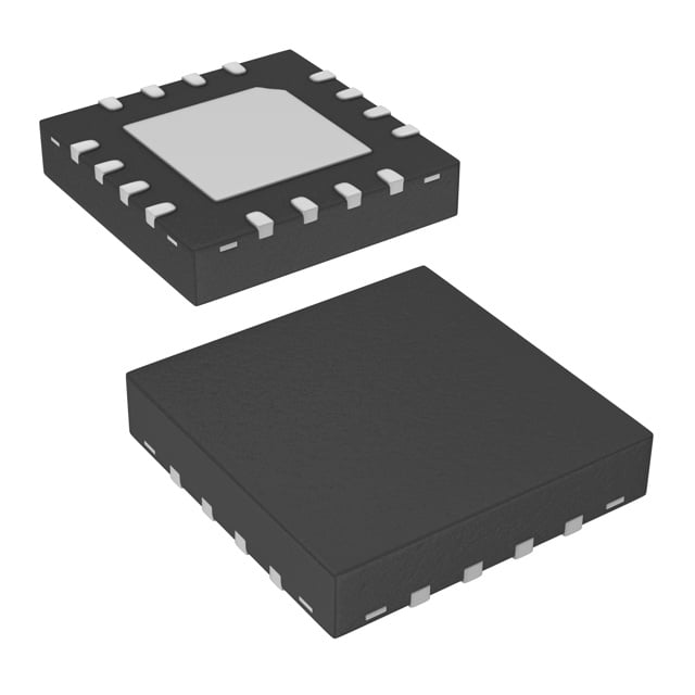
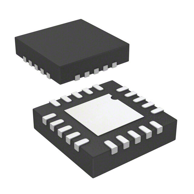
| 描述 | IC BATT CHRGR LI-ION 4.1V 16-QFN |
| 产品分类 | |
| 品牌 | Intersil |
| 数据手册 | |
| 产品图片 |
|
| 产品型号 | ISL6292-1CR4Z |
| PCN设计/规格 | |
| rohs | 无铅 / 符合限制有害物质指令(RoHS)规范要求 |
| 产品系列 | - |
| 供应商器件封装 | 16-QFN-EP(4x4) |
| 功能 | 充电管理 |
| 包装 | 管件 |
| 安装类型 | 表面贴装 |
| 封装/外壳 | 16-VQFN 裸露焊盘 |
| 工作温度 | -20°C ~ 70°C |
| 标准包装 | 75 |
| 电压-电源 | 4.3 V ~ 6.5 V |
| 电池化学 | 锂离子,锂聚合物 |


- 商务部:美国ITC正式对集成电路等产品启动337调查
- 曝三星4nm工艺存在良率问题 高通将骁龙8 Gen1或转产台积电
- 太阳诱电将投资9.5亿元在常州建新厂生产MLCC 预计2023年完工
- 英特尔发布欧洲新工厂建设计划 深化IDM 2.0 战略
- 台积电先进制程称霸业界 有大客户加持明年业绩稳了
- 达到5530亿美元!SIA预计今年全球半导体销售额将创下新高
- 英特尔拟将自动驾驶子公司Mobileye上市 估值或超500亿美元
- 三星加码芯片和SET,合并消费电子和移动部门,撤换高东真等 CEO
- 三星电子宣布重大人事变动 还合并消费电子和移动部门
- 海关总署:前11个月进口集成电路产品价值2.52万亿元 增长14.8%


PDF Datasheet 数据手册内容提取
DATASHEET ISL6292 FN9105 Li-ion/Li Polymer Battery Charger Rev.10.00 Nov.3.20 The ISL6292 is an integrated single-cell Li-ion or Li-polymer Features battery charger capable of operating with an input voltage as • Complete Charger for Single-Cell Li-ion Batteries low as 2.4V. This charger is designed to work with various types of AC adapters or a USB port. • Very Low Thermal Dissipation The ISL6292 operates as a linear charger when the AC • Integrated Pass Element and Current Sensor adapter is a voltage source. The battery is charged in a • No External Blocking Diode Required CC/CV (constant current/constant voltage) profile. The charge current is programmable with an external resistor up • 1% Voltage Accuracy to 2A. The ISL6292 can also work with a current-limited • Programmable Current Limit up to 2A adapter to minimize the thermal dissipation, in which case, • Programmable End-of-Charge Current the ISL6292 combines the benefits of both a linear charger and a pulse charger. • Charge Current Thermal Foldback The ISL6292 features charge current thermal foldback to • NTC Thermistor Interface for Battery Temperature Monitor guarantee safe operation when the printed circuit board is • Accepts Multiple Types of Adapters or USB BUS Power space limited for thermal dissipation. Additional features • Ensured to Operate at 2.65V After Start-Up include preconditioning of an over-discharged battery, an NTC thermistor interface for charging the battery in a safe • Ambient Temperature Range: -20°C to +70°C temperature range, automatic recharge, and thermally • Thermally-Enhanced QFN Packages enhanced QFN or DFN packages. • Handheld Devices, including Medical Handhelds Related Literature • PDAs, Cell Phones and Smart Phones For a full list of related documents, visit our website • Portable Instruments, MP3 Players • ISL6292 product page • Self-Charging Battery Packs • Stand-Alone Chargers • USB Bus-Powered Chargers • Pb-Free Available (RoHS Compliant) FN9105 Rev.10.00 Page 1 of 22 Nov.3.20
ISL6292 Overview Typical Applications 5V Wall VIN VBAT Adapter 1F TOEN 1F C 1k 1k C V2P8 1 R1 R2 2 Battery Pack ISL6292 R D D U RT T 1 2 TEMP FAULT STATUS IREF IMIN EN R R V2P8 IMIN IREF TIME GND 80k 80k 1F C C 3 TIME 15nF FIGURE 1. TYPICAL APPLICATION CIRCUIT FOR 4X5 OR 5X5 QFN PACKAGE OPTIONS 5V Wall VIN VBA T Adapter 1F 1F C1 1k 1k C2 BaBttaetrtyery R R Pac 1 2 ISL6292 Pack k D1 D2 (3X3 DFN) RT T TEMP FAULT R STATUS U V2P8 EN IREF 1F TIME GND R C IREF 3 80k C TIME 15nF FIGURE 2. TYPICAL APPLICATION CIRCUIT FOR 3X3 DFN PACKAGE OPTION FN9105 Rev.10.00 Page 2 of 22 Nov.3.20
ISL6292 Block Diagram Q VIN MAIN VBAT C 1 References V2P8 Temperature Monitoring QSEN 100000:1 Current R H N G I Mirror VPO VC VMI ECHR T I VR VIN VBAT SEN Input_OK + - V POR + IREF IR C-A + -+100mV - R IREF Current CHRG References IMIN + IMIN VA- R V IMIN CH + Trickle/Fast Minbat - ISEN VMIN + V RECHRG - MIN_I + - V2P8 Recharge STATUS Under Temp LOGIC STATUS NTC Over Temp TEMP Interface Batt Removal FAULT FAULT TOEN TIME OSC COUNTER Input_OK GND EN NOTE: For the 3x3 DFN package, the TOEN pin is left floating and the IMIN pin is connected to the V2P8 pin internally. FIGURE 3. BLOCK PROGRAM FN9105 Rev.10.00 Page 3 of 22 Nov.3.20
ISL6292 Ordering Information PART NUMBER TAPE AND REEL PACKAGE PKG. (Notes2, 3) PART MARKING TEMP. RANGE (°C) (Units) (Note1) (RoHS Compliant) DWG.# ISL6292-1CR3Z 921Z -20 to +70 - 10 Ld 3x3 DFN L10.3x3 ISL6292-1CR3Z-T 921Z -20 to +70 6k 10 Ld 3x3 DFN L10.3x3 ISL6292-2CR3Z 922Z -20 to +70 - 10 Ld 3x3 DFN L10.3x3 ISL6292-2CR3Z-T 922Z -20 to +70 6k 10 Ld 3x3 DFN L10.3x3 ISL6292-1CR4Z 629 21CR4Z -20 to +70 - 16 Ld 4x4 QFN L16.4x4 ISL6292-1CR4Z-T 629 21CR4Z -20 to +70 6k 16 Ld 4x4 QFN L16.4x4 ISL6292-2CR4Z 629 22CR4Z -20 to +70 - 16 Ld 4x4 QFN L16.4x4 ISL6292-2CR4Z-T 629 22CR4Z -20 to +70 6k 16 Ld 4x4 QFN L16.4x4 ISL6292-1CR5Z 6292-1CR5Z -20 to +70 - 16 Ld 5x5 QFN L16.5x5B ISL6292-1CR5Z-T 6292-1CR5Z -20 to +70 6k 16 Ld 5x5 QFN L16.5x5B ISL6292-2CR5Z 6292-2CR5Z -20 to +70 - 16 Ld 5x5 QFN L16.5x5B ISL6292-2CR5Z-T 6292-2CR5Z -20 to +70 6k 16 Ld 5x5 QFN L16.5x5B ISL6292EVAL1Z Evaluation Board for the 3x3 DFN Package Part ISL6292EVAL2Z Evaluation Board for the 4x4 QFN Package Part NOTES: 1. See TB347 for details about reel specifications. 2. These Pb-free plastic packaged products employ special Pb-free material sets, molding compounds/die attach materials, and 100% matte tin plate plus anneal (e3 termination finish, which is RoHS compliant and compatible with both SnPb and Pb-free soldering operations). Pb-free products are MSL classified at Pb-free peak reflow temperatures that meet or exceed the Pb-free requirements of IPC/JEDEC J-STD-020. 3. For Moisture Sensitivity Level (MSL), see the ISL6292 device page. For more information about MSL, see TB363. FN9105 Rev.10.00 Page 4 of 22 Nov.3.20
ISL6292 Pin Configuration ISL6292 ISL6292 (16 LD QFN) (10 LD DFN) TOP VIEW TOP VIEW T T A A VIN VIN VB VB VIN 1 10 VBAT 16 15 14 13 FAULT 2 9 TEMP VIN 1 12 VBAT STATUS 3 8 IREF FAULT 2 11 TEMP TIME 4 7 V2P8 STATUS 3 10 IMIN GND 5 6 EN TIME 4 9 IREF 5 6 7 8 D N N 8 N E E P G TO V2 Pin Descriptions EN (Pin 7 for 4x4, 5x5; Pin 6 for 3x3) VIN (Pin 1, 15, 16 for 4x4, 5x5; Pin 1 for 3x3) EN is the enable logic input. Connect the EN pin to LOW to VIN is the input power source. Connect to a wall adapter. disable the charger or leave it floating to enable the charger. FAULT (Pin 2) V2P8 (Pin 8 for 4x4, 5x5; Pin 7 for 3x3) FAULT is an open-drain output indicating fault status. This This is a 2.8V reference voltage output. This pin outputs a pin is pulled to LOW under any fault conditions. 2.8V voltage source when the input voltage is above POR threshold and outputs zero otherwise. The V2P8 pin can be STATUS (Pin 3) used as an indication for adapter presence. STATUS is an open-drain output indicating charging and IREF(Pin 9 for 4x4, 5x5; Pin 8 for 3x3) inhibit states. The STATUS pin is pulled LOW when the This is the programming input for the constant charging charger is charging a battery. current. Time (Pin 4) IMIN (Pin 10 for 4x4, 5x5; N/A for 3x3) The TIME pin determines the oscillation period by IMIN is the programmable input for the end-of-charge connecting a timing capacitor between this pin and GND. current. The oscillator also provides a time reference for the charger. TEMP (Pin 11 for 4x4, 5x5; Pin 9 for 3x3) GND (Pin 5) TEMP is the input for an external NTC thermistor. The TEMP GND is the connection to system ground. pin is also used for battery removal detection. TOEN (Pin 6 for 4x4, 5x5; N/A for 3x3) VBAT (Pin 12, 13, 14 for 4x4, 5x5; Pin 10 for 3x3) TOEN is the TIMEOUT enable input pin. Pulling this pin to VBAT is the connection to the battery. Typically a 10µF LOW disables the TIMEOUT charge-time limit for the fast Tantalum capacitor is needed for stability when there is no charge modes. Leaving this pin HIGH or floating enables the battery attached. When a battery is attached, only a 0.1µF TIMEOUT limit. ceramic capacitor is required. FN9105 Rev.10.00 Page 5 of 22 Nov.3.20
ISL6292 Absolute Maximum Ratings Thermal Information Supply Voltage (VIN) . . . . . . . . . . . . . . . . . . . . . . . . . . . .-0.3V to 7V Thermal Resistance (Junction to Ambient) JA (°C/W) JC (°C/W) Output Pin Voltage (BAT). . . . . . . . . . . . . . . . . . . . . . . -0.3V to 5.5V 5x5 QFN Package (Notes 4, 5) . . . . . . 34 4 Signal Input Voltage (TOEN, TIME, IREF, IMIN) . . . . . -0.3V to 3.2V 4x4 QFN Package (Notes 4, 5) . . . . . . 41 4 Output Pin Voltage (STATUS, FAULT). . . . . . . . . . . . . . .-0.3V to 7V 3x3 DFN Package (Notes 4, 5) . . . . . . 46 4 Charge Current (For 4x4 or 5x5 QFN Packages) . . . . . . . . . . . 2.1A Maximum Junction Temperature (Plastic Package) . . . . . . .+150°C Charge Current (For 3x3 DFN Package) . . . . . . . . . . . . . . . . . 1.6A Maximum Storage Temperature Range. . . . . . . . . .-65°C to +150°C Pb-free reflow profile . . . . . . . . . . . . . . . . . . . . . . . . . . . . see TB493 Recommended Operating Conditions Ambient Temperature Range. . . . . . . . . . . . . . . . . . .-20°C to +70°C Supply Voltage, VIN. . . . . . . . . . . . . . . . . . . . . . . . . . . 4.3V to 6.5V CAUTION: Do not operate at or near the maximum ratings listed for extended periods of time. Exposure to such conditions can adversely impact product reliability and result in failures not covered by warranty. NOTES: 4. JA is measured in free air with the component mounted on a high-effective thermal conductivity test board with direct attach features. See TB379. 5. JC, case temperature location is at the center of the exposed metal pad on the package underside. See TB379. Electrical Specifications Typical values are tested at VIN = 5V and +25°C Ambient Temperature, maximum and minimum values are guaranteed over 0°C to +70°C Ambient Temperature with a supply voltage in the range of 4.3V to 6.5V, unless otherwise noted. PARAMETER SYMBOL TEST CONDITIONS MIN TYP MAX UNITS POWER-ON RESET Rising VIN Threshold 3.0 3.4 4.0 V Falling VIN Threshold 2.11 2.4 2.65 V STANDBY CURRENT VBAT Pin Sink Current ISTANDBY VIN floating or EN = LOW - - 3.0 µA VIN Pin Supply Current IVIN VBAT floating and EN pulled low - 30 - µA VIN Pin Supply Current IVIN VBAT floating and EN floating - 1 - mA VOLTAGE REGULATION Output Voltage VCH ISL6292-1 4.059 4.10 4.141 V Output Voltage VCH ISL6292-2 4.158 4.20 4.242 V Dropout Voltage VBAT = 3.7V, 0.5A, 4x4 or 5x5 package - 140 - mV Dropout Voltage VBAT = 3.7V, 0.5A, 3x3 package - 175 - mV CHARGE CURRENT Constant Charge Current ICHARGE RIREF = 80k, VBAT = 3.7V 0.9 1.0 1.1 A Trickle Charge Current ITRICKLE RIREF = 80k, VBAT = 2.0V - 110 - mA Constant Charge Current ICHARGE IREF Pin Voltage > 1.2V, VBAT = 3.7V 400 450 520 mA Trickle Charge Current ITRICKLE IREF Pin Voltage > 1.2V, VBAT = 2.0V - 45 - mA Constant Charge Current ICHARGE IREF Pin Voltage < 0.4V, VBAT = 3.7V - - 100 mA Trickle Charge Current ITRICKLE IREF Pin Voltage < 0.4V, VBAT = 2.0V - 10 - mA End-of-Charge Threshold RIMIN = 80k 85 110 135 mA RECHARGE THRESHOLD Recharge Voltage Threshold VRECHRG ISL6292-2 - 4.0 - V Recharge Voltage Threshold VRECHRG ISL6292-1 - 3.90 - V FN9105 Rev.10.00 Page 6 of 22 Nov.3.20
ISL6292 Electrical Specifications Typical values are tested at VIN = 5V and +25°C Ambient Temperature, maximum and minimum values are guaranteed over 0°C to +70°C Ambient Temperature with a supply voltage in the range of 4.3V to 6.5V, unless otherwise noted. (Continued) PARAMETER SYMBOL TEST CONDITIONS MIN TYP MAX UNITS TRICKLE CHARGE THRESHOLD Trickle Charge Threshold Voltage VMIN 2.7 2.8 3.0 V TEMPERATURE MONITORING Low Battery Temperature Threshold VTMIN V2P8 = 3.0V 1.45 1.51 1.57 V High Battery Temperature Threshold VTMAX V2P8 = 3.0V 0.36 0.38 0.40 V Battery Removal Threshold VRMV V2P8 = 3.0V - 2.25 - V Charge Current Foldback Threshold TFOLD 85 100 115 °C Current Foldback Gain GFOLD - 100 - mA/°C OSCILLATOR Oscillation Period tOSC CTIME = 15nF 2.4 3.0 3.6 ms LOGIC INPUT AND OUTPUT TOEN Input High 2.0 - - V TOEN and EN Input Low - - 0.8 V IREF and IMIN Input High 1.2 - - V IREF and IMIN Input Low - - 0.4 V STATUS/FAULT Sink Current Pin Voltage = 0.8V 5 - - mA Typical Operating Performance The test conditions for the Typical Operating Performance are: VIN = 5V, TA = +25°C, RIREF = RIMIN = 80k, VBAT = 3.7V, Unless Otherwise Noted. 4.2015 4.210 4.208 4.2010 4.206 CHARGE CURRENT = 50mA 4.2005 RIREF = 40k 4.204 4.2000 4.202 V) V) (AT 4.1995 (AT 4.200 B B V V 4.198 4.1990 4.196 4.1985 4.194 4.1980 4.192 4.1975 4.190 0 0.3 0.6 0.9 1.2 1.5 0 20 40 60 80 100 120 CHARGE CURRENT (A) TEMPERATURE (°C) FIGURE 4. CHARGER OUTPUT VOLTAGE vs CHARGE FIGURE 5. CHARGER OUTPUT VOLTAGE vs TEMPERATURE CURRENT FN9105 Rev.10.00 Page 7 of 22 Nov.3.20
ISL6292 Typical Operating Performance The test conditions for the Typical Operating Performance are: VIN = 5V, TA = +25°C, RIREF = RIMIN = 80k, VBAT = 3.7V, Unless Otherwise Noted. (Continued) 4.30 2.0 2A 1.8 CHARGE CURRENT = 50mA 1.6 4.25 A) 1.5A T ( 1.4 N E 1.2 (V)T 4.20 URR 1.0 1A A C VB GE 0.8 R 0.5A A 0.6 4.15 H C 0.4 USB500 0.2 USB100 4.10 0 4.2 4.5 4.8 5.1 5.4 5.7 6.0 6.3 3.0 3.2 3.4 3.6 3.8 4.0 VIN (V) VBAT (V) FIGURE 6. CHARGER OUTPUT VOLTAGE vs INPUT FIGURE 7. CHARGE CURRENT vs OUTPUT VOLTAGE VOLTAGE CHARGE CURRENT = 50mA 1.6 2.0 1.8 1.4 1.5A 1.6 CHARGE CURRENT (A) 00011.....46802 0.5A 1.0A CHARGE CURRENT (A) 000111......468024 0. 15 . A5 A 1A 2 A USB500 0.2 0.2 US B 100 0.0 0 0 20 40 60 80 100 120 4.3 4.5 4.7 4.9 5.1 5.3 5.5 5.7 5.9 6.1 6.3 6.5 TEMPERATURE (°C) VIN (V) FIGURE 8. CHARGE CURRENT vs AMBIENT TEMPERATURE FIGURE 9. CHARGE CURRENT vs INPUT VOLTAGE 2.930 3.00 2.95 2.928 V2P8 PIN LOADED WITH 2mA )V( EG 2.926 )V( EG 2.90 ATLO ATLO 2.85 V 8P2V 2.924 V 8P2V 2.80 2.922 2.75 2.920 2.70 3.5 4.0 4.5 5.0 5.5 6.0 6.5 0 2 4 6 8 10 VIN (V) V2P8 LOAD CURRENT (mA) FIGURE 10. V2P8 OUTPUT vs INPUT VOLTAGE FIGURE 11. V2P8 OUTPUT vs ITS LOAD CURRENT FN9105 Rev.10.00 Page 8 of 22 Nov.3.20
ISL6292 Typical Operating Performance The test conditions for the Typical Operating Performance are: VIN = 5V, TA = +25°C, RIREF = RIMIN = 80k, VBAT = 3.7V, Unless Otherwise Noted. (Continued) 700 420 500mA CHARGE CURRENT, 650 THERMAL FOLDBACK STARTS NEAR +100°C 400 RIREF = 40k 600 380 550 ) 500 ) 360 m m 3x3 DFN (ON) 450 (ON) 340 rDS( 345000 3x3 DFN rDS( 320 4x 4 QFN 300 300 4x4 QFN 280 250 200 260 0 20 40 60 80 100 120 3.0 3.2 3.4 3.6 3.8 4.0 TEMPERATURE (°C) VBAT (V) FIGURE 12. rDS(ON) vs TEMPERATURE AT 3.7V OUTPUT FIGURE 13. rDS(ON) vs OUTPUT VOLTAGE USING CURRENT LIMITED ADAPTERS 1.8 50 A) 1.6 A) 45 EN = GND T (µ 1.4 T (µ 40 REN 1.2 REN 35 R R 30 CU 1.0 CU E T 25 G 0.8 N LEAKA 0.6 UIESCE 1250 V BAT 00..24 V QIN 105 0.0 0 0 20 40 60 80 100 120 0 20 40 60 80 100 120 TEMPERATURE (°C) TEMPERATURE (°C) FIGURE 14. REVERSE CURRENT vs TEMPERATURE FIGURE 15. INPUT QUIESCENT CURRENT vs TEMPERATURE 32 1.10 30 EN = GND A) CURRENT (µA) 22222468 T CURRENT (m 011...900505 ESCENT 112680 UIESCEN 0.90 BPIONTSH F VLBOAATT IANNGD EN UI Q Q 14 N 0.85 N VI VI 12 10 0.80 3.0 3.5 4.0 4.5 5.0 5.5 6.0 6.5 4.3 4.6 4.9 5.2 5.5 5.8 6.1 6.4 VIN (V) VIN (V) FIGURE 16. INPUT QUIESCENT CURRENT vs INPUT FIGURE 17. INPUT QUIESCENT CURRENT vs INPUT VOLTAGE WHEN SHUTDOWN VOLTAGE WHEN NOT SHUTDOWN FN9105 Rev.10.00 Page 9 of 22 Nov.3.20
ISL6292 Typical Operating Performance The test conditions for the Typical Operating Performance are: VIN = 5V, TA = +25°C, RIREF = RIMIN = 80k, VBAT = 3.7V, Unless Otherwise Noted. (Continued) 28 24 A) m 20 T ( N E 16 R R U C 12 N PI S 8 U T A T 4 S 0 0.0 0.5 1.0 1.5 2.0 2.5 3.0 3.5 4.0 4.5 5.0 STATUS PIN VOLTAGE (V) FIGURE 18. STATUS/FAULT PIN VOLTAGE vs CURRENT WHEN THE OPEN-DRAIN MOSFET TURNS ON FN9105 Rev.10.00 Page 10 of 22 Nov.3.20
ISL6292 Theory of Operation The charger automatically re-charges the battery when the battery voltage drops below a recharge threshold. When the The ISL6292 is an integrated charger for single-cell Li-ion or wall adapter is not present, the ISL6292 draws less than 1µA Li-polymer batteries. The ISL6292 functions as a traditional current from the battery. linear charger when powered with a voltage-source adapter. When powered with a current-limited adapter, the charger Three indication pins are available from the charger to minimizes the thermal dissipation commonly seen in indicate the charge status. The V2P8 outputs a 2.8VDC traditional linear chargers. voltage when the input voltage is above the power-on reset (POR) level and can be used as the power-present As a linear charger, the ISL6292 charges a battery in the indication. This pin is capable of sourcing a 2mA current, so popular constant current (CC) and constant voltage (CV) it can also be used to bias external circuits. The STATUS pin profile. The constant charge current IREF is programmable up is an open-drain logic output that turns LOW at the beginning to 2A (1.5A for the 3x3 DFN package) with an external resistor of a charge cycle until the end-of-charge (EOC) condition is or a logic input. The charge voltage VCH has 1% accuracy qualified. The EOC condition is: the battery voltage rises over the entire recommended operating condition range. The above the recharge threshold and the charge current falls charger always preconditions the battery with 10% of the below a user-programmable EOC current threshold. Once programmed current at the beginning of a charge cycle, until the EOC condition is qualified, the STATUS output rises to the battery voltage is verified to be above the minimum fast HIGH and is latched. The latch is released at the beginning charge voltage, VMIN. This low-current preconditioning of a charge or re-charge cycle. The open-drain FAULT pin charge mode is named trickle mode. The verification takes 15 turns low when any fault conditions occur. The fault cycles of an internal oscillator whose period is programmable conditions include the external battery temperature fault, a with the timing capacitor. A thermal-foldback feature removes charge time fault, or the battery removal. the thermal concern typically seen in linear chargers. The charger reduces the charge current automatically as the IC Figure 19 shows the typical charge curves in a traditional internal temperature rises above +100°C to prevent further linear charger powered with a constant-voltage adapter. temperature rise. The thermal-foldback feature guarantees From top to bottom, the curves represent the constant input safe operation when the printed circuit board (PCB) is space voltage, the battery voltage, the charge current and the limited for thermal dissipation. power dissipation in the charger. The power dissipation PCH is given by Equation 1: A TEMP pin monitors the battery temperature to ensure a safe charging temperature range. The temperature range is PCH = VIN-VBATICHARGE (EQ. 1) programmable with an external negative temperature coefficient (NTC) thermistor. The TEMP pin is also used to where ICHARGE is the charge current. The maximum power dissipation occurs during the beginning of the CC mode. The detect the removal of the battery. maximum power the IC is capable of dissipating is The charger offers a safety timer for setting the fast charge time dependent on the thermal impedance of the printed-circuit (TIMEOUT) limit to prevent charging a dead battery for an board (PCB). Figure 19 shows (with dotted lines) two cases extensively long time. The TIMEOUT limit can be disabled as that the charge currents are limited by the maximum power needed by the TOEN pin. The trickle mode is limited to 1/8 of dissipation capability due to the thermal foldback. TIMEOUT and cannot be disabled by the TOEN pin. Trickle Constant Current Constant Voltage Inhibit Mode Mode Mode Trickle Constant Current Constant Voltage Inhibit Mode Mode Mode V Input Voltage IN V V VIN Input Voltage CH Battery Voltage CH Battery Voltage V MIN V MIN I REF I REF I LIM Charge Current Charge Current I /10 I /10 REF REF P 1 P 2 P3 Power Dissipation P1 Power Dissipation P 2 TIMEOUT TIMEOUT FIGURE 19. TYPICAL CHARGE CURVES USING A FIGURE 20. TYPICAL CHARGE CURVES USING A CURRENT- CONSTANT-VOLTAGE ADAPTER LIMITED ADAPTER FN9105 Rev.10.00 Page 11 of 22 Nov.3.20
ISL6292 When using a current-limited adapter, the thermal situation The two indication pins, STATUS and FAULT, indicate a in the ISL6292 is totally different. Figure 20 shows the typical LOW and a HIGH logic signal respectively. Figure 21 charge curves when a current-limited adapter is employed. illustrates the start-up of the charger between t0 to t2. The operation requires the IREF to be programmed higher The ISL6292 has a typical rising POR threshold of 3.4V and than the limited current ILIM of the adapter, as shown in a falling POR threshold of 2.4V. The 2.4V falling threshold Figure 20. The key difference of the charger operating under guarantees charger operation with a current-limited adapter such conditions occurs during the CC mode. to minimize the thermal dissipation. The Block Diagram (Figure 3) aids in understanding the Charge Cycle operation. The current loop consists of the current amplifier CA and the sense MOSFET QSEN. The current reference IR A charge cycle consists of three charge modes: trickle mode, is programmed by the IREF pin. The current amplifier CA constant current (CC) mode, and constant voltage (CV) mode. regulates the gate of the sense MOSFET QSEN so that the The charge cycle always starts with the trickle mode until the sensed current ISEN matches the reference current IR. The battery voltage stays above VMIN (2.8V typical) for 15 main MOSFET QMAIN and the sense MOSFET QSEN form a consecutive cycles of the internal oscillator. If the battery current mirror with a ratio of 100,000:1, that is, the output voltage drops below VMIN during the 15 cycles, the 15-cycle charge current is 100,000 times IR. In the CC mode, the counter is reset and the charger stays in the trickle mode. The charger moves to the CC mode after verifying the battery current loop tries to increase the charge current by enhancing the sense MOSFET QSEN, so that the sensed voltage. As the battery-pack terminal voltage rises to the final current matches the reference current. On the other hand, charge voltage VCH, the CV mode begins. The terminal the adapter current is limited, the actual output current will voltage is regulated at the constant VCH in the CV mode and never meet what is required by the current reference. As a the charge current is expected to decline. After the charge result, the current error amplifier CA keeps enhancing the current drops below IMIN (programmable for the 4x4 and 5x5 QSEN as well as the main MOSFET QMAIN, until they are package and programmed to 1/10 of IREF for the 3x3 fully turned on. Therefore, the main MOSFET becomes a package; see “End-of-Charge (EOC) Current” on page14 for power switch instead of a linear regulation device. The more detail), the ISL6292 indicates the end-of-charge (EOC) power dissipation in the CC mode becomes Equation 2: with the STATUS pin. The charging actually does not 2 terminate until the internal timer completes its length of P = r I CH DSON CHARGE (EQ. 2) TIMEOUT in order to bring the battery to its full capacity. Signals in a charge cycle are illustrated in Figure 21 between where rDS(ON) is the resistance when the main MOSFET is points t2 to t5. fully turned on. This power is typically much less than the peak power in the traditional linear mode. The worst power dissipation when using a current-limited VIN adapter typically occurs at the beginning of the CV mode, as POR Threshold shown in Figure 20. Equation 1 applies during the CV mode. V2P8 When using a very small PCB whose thermal impedance is Charge Cycle Charge Cycle relatively large, it is possible that the internal temperature can still reach the thermal foldback threshold. In that case, STATUS the IC is thermally protected by lowering the charge current, as shown with the dotted lines in the charge current and 15 Cycles to power curves. Appropriate design of the adapter can further FAULT 1/8 TIMEOUT reduce the peak power dissipation of the ISL6292. See“Applications Information” on page12 for more VBAT VRECHRG 15 Cycles information. 2.8V V MIN Figure 21 illustrates the typical signal waveforms for the I I MIN linear charger from the power-up to a recharge cycle. More CHARGE detailed Applications Information is given in the following. t t t t t t t t t 0 1 2 3 4 5 6 7 8 Applications Information FIGURE 21. OPERATION WAVEFORMS Power on Reset (POR) The ISL6292 resets itself as the input voltage rises above the POR rising threshold. The V2P8 pin outputs a 2.8V voltage, the internal oscillator starts to oscillate, the internal timer is reset, and the charger begins to charge the battery. FN9105 Rev.10.00 Page 12 of 22 Nov.3.20
ISL6292 The following events initiate a new charge cycle: Disabling TIMEOUT Limit • POR, The TIMEOUT limit for the fast charge modes can be disabled by pulling the TOEN pin to LOW or shorting it to GND. When • a new battery being inserted (detected by TEMP pin), this happens, the charger becomes a current-limited LDO • the battery voltage drops below a recharge threshold after (low-dropout) supply with its voltage regulated at the final completing a charge cycle, charge voltage VCH and the current limit determined by the IREF pin. If the LDO load current drops below the end-of- • recovery from an battery over-temperature fault, charge current (refer to “End-of-Charge (EOC) Current” on • or, the EN pin is toggled from GND to floating. page14), the STATUS pin will indicate. Further description of these events are given later in this The trickle charge time limit, however, is not disabled even data sheet. when the TOEN pin is pulled to LOW. The charger operates Recharge in the trickle mode at the beginning of a charge cycle even if the TIMEOUT is disabled. Leaving the TOEN pin floating is After a charge cycle completes, charging is prohibited until recommended to enable the TIMEOUT. Driving the TOEN the battery voltage drops to a recharge threshold, VRECHRG pin above 3.0V is not recommended. (see “Electrical Specifications” on page6). Then a new charge cycle starts at point t6 and ends at point t8, as shown Charge Current Programming in Figure 21. The safety timer is reset at t6. The charge current is programmed by the IREF pin. There Internal Oscillator are three ways to program the charge current: The internal oscillator establishes a timing reference. The 1. Driving the IREF pin above 1.3V oscillation period is programmable with an external timing 2. Driving the IREF pin below 0.4V, capacitor, CTIME, as shown in Typical Applications. The 3. or using the RIREF as shown in “Theory of Operation” on oscillator charges the timing capacitor to 1.5V and then page11. discharges it to 0.5V in one period, both with 10µA current. The voltage of IREF is regulated to a 0.8V reference voltage The period tOSC is: when not driven by any external source. The charging 6 tOSC = 0.210 CTIME seconds current during the constant current mode is 100,000 times (EQ. 3) that of the current in the RIREF resistor. Hence, depending A 1nF capacitor results in a 0.2ms oscillation period. The on how IREF pin is used, the charge current is: accuracy of the period is mainly dependent on the accuracy V 1.3V 500mA IREF of the capacitance and the internal current source. 0.8V 5 Total Charge Time IREF= R-----I--R----E----F--10 A RIREF (EQ. 5) 100mA V 0.4V The total charge time for the CC mode and CV mode is IREF limited to a length of TIMEOUT. A 22-stage binary counter The 500mA current is a guaranteed maximum value for the increments each oscillation period of the internal oscillator to high-power USB port, with the typical value of 450mA. The set the TIMEOUT. The TIMEOUT can be calculated as: 100mA current is also a guaranteed maximum value for the TIMEOUT = 222t = 14C-----T----I--M----E--- minutes (EQ. 4) low-power USB port. This design accommodates the USB OSC 1nF power specification. The internal reference voltage at the IREF pin is capable of A 1nF capacitor leads to 14 minutes of TIMEOUT. For sourcing less than 100µA current. When pulling down the example, a 15nF capacitor sets the TIMEOUT to be IREF pin with a logic circuit, the logic circuit needs to be able 3.5 hours. The charger has to reach the end-of-charge to sink at least 100µA current. condition before the TIMEOUT, otherwise, a TIMEOUT fault When the adapter is current limited, it is recommended that is issued. The TIMEOUT fault latches up the charger. There the reference current be programmed to at least 30% higher are two ways to release such a latch-up: either to recycle the than the adapter current limit (which equals the charge input power, or toggle the EN pin to disable the charger and current). In addition, the charge current should be at least then enable it again. 350mA so that the voltage difference between the VIN and The trickle mode charge has a time limit of 1/8 TIMEOUT. If the VBAT pins is higher than 100mV. The 100mV is the the battery voltage does not reach VMIN within this limit, a offset voltage of the input-output voltage comparator shown TIMEOUT fault is issued and the charger latches up. The in the block diagram on page3. charger stays in trickle mode for at least 15 cycles of the internal oscillator and, at most, 1/8 of TIMEOUT, as shown in Figure 21. FN9105 Rev.10.00 Page 13 of 22 Nov.3.20
ISL6292 End-of-Charge (EOC) Current happen) the charger does not indicate end-of-charge unless the battery voltage is already above the recharge threshold. The end-of-charge current IMIN sets the level at which the charger starts to indicate the end of the charge with the 2.8V Bias Voltage STATUS pin, as shown in Figure 21. The charger actually The ISL6292 provides a 2.8V voltage for biasing the internal does not terminate charging until the end of the TIMEOUT, control and logic circuit. This voltage is also available for as described in “Total Charge Time” on page13. The IMIN is external circuits such as the NTC thermistor circuit. The set in two ways, by connecting a resistor between the IMIN maximum allowed external load is 2mA. pin and ground, or by connecting the IMIN pin to the V2P8 pin. When programming with the resistor, the IMIN is set in NTC Thermistor Equation 6. The ISL6292 uses two comparators (CP2 and CP3) to form a I = 10000-V----R-----E---F---= ---0---.--8---V-----104A window comparator, as shown in Figure 24. When the TEMP MIN R R (EQ. 6) IMIN IMIN pin voltage is “out of the window,” determined by the VTMIN where RIMIN is the resistor connected between the IMIN pin and VTMAX, the ISL6292 stops charging and indicates a fault and the ground. When connected to the V2P8 pin, the IMIN condition. When the temperature returns to the set range, the is set to 1/10 of IREF, except when the IREF pin is shorted to charger re-starts a charge cycle. The two MOSFETs, Q1 and GND. Under this exception, IMIN is 5mA. For the ISL6292 in Q2, produce hysteresis for both upper and lower thresholds. the 3x3 DFN package, the IMIN pin is bonded internally to The temperature window is shown in Figure 23. V2P8. 2.8V Charge Current Thermal Foldback Over-heating is always a concern in a linear charger. The V (1.4V) maximum power dissipation usually occurs at the beginning TMIN V (1.2V) of a charge cycle when the battery voltage is at its minimum TMIN- TEMP but the charge current is at its maximum. The charge current Pin Voltage thermal foldback function in the ISL6292 frees users from the over-heating concern. V (0.406V) TMAX+ Figure 22 shows the current signals at the summing node of V (0.35V) TMAX the current error amplifier CA in the Block Diagram shown on 0V page3. IR is the reference and IT is the current from the Temperature Monitoring block. The IT has no impact on the UTnemdepr charge current until the internal temperature reaches Over approximately +100°C; then IT rises at a rate of 1µA/°C. Temp When IT rises, the current control loop forces the sensed FIGURE 23. CRITICAL VOLTAGE LEVELS FOR TEMP PIN current ISEN to reduce at the same rate. As a mirrored current, the charge current is 100,000 times that of the 2.8V sensed current and reduces at a rate of 100mA/°C. For a V2P8 ISL6292 charger with the constant charge current set at 1A, the R1 charge current is reduced to zero when the internal Battery CP1 - VRMV 40K Removal temperature rises to +110°C. The actual charge current + R2 settles between +100°C to +110°C. 60K RU UTenmdepr CP2 - VTMIN R3 IR + To TEMP Pin 75K TEMP I Q1 T OTevmerp CP3 - R254K RT + VTMAX I SEN Q2 R5 4K GND 100OC Temperature FIGURE 22. CURRENT SIGNALS AT THE AMPLIFIER CA INPUT FIGURE 24. THE INTERNAL AND EXTERNAL CIRCUIT FOR THE NTC INTERFACE Usually the charge current should not drop below IMIN because As the TEMP pin voltage rises from low and exceeds the 1.4V of the thermal foldback. For some extreme cases (if that does threshold, the under temperature signal rises and does not clear until the TEMP pin voltage falls below the 1.2V falling FN9105 Rev.10.00 Page 14 of 22 Nov.3.20
ISL6292 threshold. Similarly, the over-temperature signal is given when where the 0.039 is the NTC at +47°C. the TEMP pin voltage falls below the 0.35V threshold and does For applications that do not need to monitor the battery not clear until the voltage rises above 0.406V. The actual temperature, the NTC thermistor can be replaced with a accuracy of the 2.8V is not important because all the regular resistor of a half value of the pull-up resistor RU. thresholds and the TEMP pin voltage are ratios determined by Another option is to connect the TEMP pin to the IREF pin the resistor dividers, as shown in Figure24. that has a 0.8V output. With such connection, the IREF pin The NTC thermistor is required to have a resistance ratio of can no longer be programmed with logic inputs. 7:1 at the low and the high temperature limits, that is: Battery Removal Detection R COLD -------------------- = 7 (EQ. 7) The ISL6292 assumes that the thermistor is co-packed with R HOT the battery and is removed together with the battery. When This is because at the low temperature limit, the TEMP pin the charger senses a TEMP pin voltage that is 2.1V or voltage is 1.4V, which is 1/2 of the 2.8V bias. Thus: higher, it assumes that the battery is removed. The battery RCOLD = RU (EQ. 8) removal detection circuit is also shown in Figure 24. When a battery is removed, a FAULT signal is indicated and charging where RU is the pull-up resistor as shown in Figure 24. On is halted. When a battery is inserted again, a new charge the other hand, at the high temperature limit the TEMP pin cycle starts. voltage is 0.35V, 1/8 of the 2.8V bias. Therefore: Indications R R = -----U--- (EQ. 9) The ISL6292 has three indications: the input presence, the HOT 7 charge status, and the fault indication. The input presence is Various NTC thermistors are available for this application. indicated by the V2P8 pin while the other two indications are Table 1 shows the resistance ratio and the negative presented by the STATUS pin and FAULT pin respectively. temperature coefficient of the curve-1 NTC thermistor from Figure 25 shows the V2P8 pin voltage vs the input voltage. Vishay (http://www.vishay.com) at various temperatures. The Table 2 summarizes the other two pins. resistance at +3°C is approximately seven times the resistance at +47°C, which is shown in Equation 10: R -------3-----C----- = 7 (EQ. 10) 3.4V R 47C 2.4V Therefore, if +3°C is the low temperature limit, then the high temperature limit is approximately +47°C. The pull-up resistor RU can choose the same value as the resistance at +3°C. 2.8V V IN TABLE 1. RESISTANCE RATIO OF VISHAY’S CURVE-1 NTC TEMPERATURE (°C) RT/R25°C NTC (%/°C) 0 3.266 5.1 V2P8 3 2.806 5.1 5 2.540 5.0 25 1.000 4.4 FIGURE 25. THE V2P8 PIN OUTPUT vs THE INPUT VOLTAGE AT THE VIN PIN. VERTICAL: 1V/DIV, 45 0.4368 4.0 HORIZONTAL: 100ms/DIV 47 0.4041 3.9 Shutdown 50 0.3602 3.9 The ISL6292 can be shutdown by pulling the EN pin to The temperature hysteresis can be estimated. At the low ground. When shut down, the charger draws typically less temperature, the hysteresis is approximately estimated in than 30µA current from the input power and the 2.8V output Equation 11: at the V2P8 pin is also turned off. The EN pin needs to be 1.4V-1.2V driven with an open-drain or open-collector logic output, so ThysLOW1----.-4----V---------0---.--0---5---1---3 C (EQ. 11) that the EN pin is floating when the charger is enabled. where 0.051 is the NTC at +3°C. Similarly, the high temperature hysteresis is estimated in Equation 12: 0.406V-0.35V ThysHIGH--0---.--3---5----V---------0---.--0---3---9----4 C (EQ. 12) FN9105 Rev.10.00 Page 15 of 22 Nov.3.20
ISL6292 TABLE 2. STATUS INDICATIONS The ISL6292 charger sits between the adapter and the battery. FAULT STATUS INDICATION High High Charge completed with no fault (Inhibit) or VNL C rO =(VNL - VFL)/ILIM Standby V B FL V High Low Charging in one of the three modes PACK r O Low High Fault R *Both outputs are pulled up with external resistors. VNL ILIM VCELL PACK Input and Output Capacitor Selection A Typically any type of capacitors can be used for the input I and the output. Use of a 0.47µF or higher value ceramic LIM capacitor for the input is recommended. When the battery is FIGURE 26. THE IDEAL I-V CHARACTERISTICS OF A CURRENT LIMITED ADAPTER attached to the charger, the output capacitor can be any ceramic type with the value higher than 0.1µF. However, if Working with Current-Limited Adapter there is a chance the charger will be used as an LDO linear As described earlier, the ISL6292 minimizes the thermal regulator, a 10µF tantalum capacitor is recommended. dissipation when running off a current-limited AC adapter, as Current-Limited Adapter shown in Figure 20. The thermal dissipation can be further Figure 26 shows the ideal current-voltage characteristics of reduced when the adapter is properly designed. The a current-limited adapter. VNL is the no-load adapter output following demonstrates that the thermal dissipation can be voltage and VFL is the full load voltage at the current limit minimized if the adapter output reaches the full-load output ILIM. Before its output current reaches the limit ILIM, the voltage (point B in Figure 26) before the battery pack voltage adapter presents the characteristics of a voltage source. The reaches the final charge voltage (4.1V or 4.2V). The slope rO represents the output resistance of the voltage assumptions for the following discussion are: the adapter supply. For a well regulated supply, the output resistance current limit = 750mA, the battery pack equivalent can be very small, but some adapters naturally have a resistance= 200m, and the charger ON-resistance is certain amount of output resistance. 350m. The adapter is equivalent to a current source when running When charging in the constant-current region, the pass in the constant-current region. Being a current source, its element in the charger is fully turned on. The charger is output voltage is dependent on the load, which, in this case, equivalent to the ON-resistance of the internal P-Channel is the charger and the battery. As the battery is being MOSFET. The entire charging system is equivalent to the charged, the adapter output rises from a lower voltage in the circuit shown in Figure 27A. The charge current is the current-voltage characteristics curve, such as point A, to constant current limit ILIM, and the adapter output voltage higher voltage until reaching the breaking point B, as shown can be easily found out as calculated in Equation 13: in Figure 26. V = I r +V Adapter LIM DSON PACK The adapter is equivalent to a voltage source with output (EQ. 13) resistance when running in the constant-voltage region; because of this characteristic. As the charge current drops, where VPACK is the battery pack voltage. The power the adapter output moves from point B to point C, shown in dissipation in the charger is given in Equation 2, where Figure 26. ICHARGE = ILIM. The battery pack can be approximated as an ideal cell with a A critical condition of the adapter design is that the adapter lumped-sum resistance in series, also shown in Figure 26. output reaches point B in Figure 26 at the same time as the battery pack voltage reaches the final charge voltage (4.1V or 4.2V), that is: V = I r +V Critical LIM DSON CH (EQ. 14) For example, if the final charge voltage is 4.2V, the rDS(ON) is 350m, and the current limit ILIM is 750mA, the critical adapter full-load voltage is 4.4625V. When the above condition is true, the charger enters the constant-voltage mode simultaneously as the adapter exits FN9105 Rev.10.00 Page 16 of 22 Nov.3.20
ISL6292 the current-limit mode. The equivalent charging system is pack voltage and the cell voltage during the charge. The 5.9V shown in Figure 27C. Since the charge current drops at a no-load voltage is just an example value higher than the full- higher rate in the constant-voltage mode than the increase rate load voltage. The cell voltage 4.05V uses the assumption that of the adapter voltage, the power dissipation decreases as the the pack resistance is 200m. Figure 28A illustrates the charge current decreases. Therefore, the worst case thermal adapter voltage, battery pack voltage, the charge current and dissipation occurs in the constant-current charge mode. Figure the power dissipation in the charger respectively in the time 27A shows the I-V curves of the adapter output, the battery domain. Adapter Charger Adapter Charger Adapter Charger VADAPTER RDS(ON) VPACK rO VADAPTER RDS(ON) VPACK rO VADAPTER 4.2V DC VPACK Output I V V LIM I NL I NL I R R R PACK PACK PACK V V Battery V Battery CELL Battery CELL Pack CELL Pack Pack FIGURE 27A. THE EQUIVALENT CIRCUIT IN FIGURE 27B. THE EQUIVALENT CIRCUIT IN FIGURE 27C. THE EQUIVALENT CIRCUIT WHEN THE CONSTANT CURRENT THE RESISTANCE-LIMIT THE PACK VOLTAGE REACHES REGION REGION THE FINAL CHARGE VOLTAGE FIGURE 27. THE EQUIVALENT CIRCUIT OF THE CHARGING SYSTEM WORKING WITH CURRENT LIMITED ADAPTERS If the battery pack voltage reaches 4.2V (or 4.1V) before the captured waveforms to demonstrate the operation with a adapter reaches point B in Figure 26, a voltage step is current-limited adapter. expected at the adapter output when the pack voltage reaches The waveforms in Figure 30 are the adapter output voltage the final charge voltage. As a result, the charger power (1V/div), the battery voltage (1V/div), and the charge current dissipation is also expected to have a step rise. This case is (200mA/div) respectively. The time scale is 1ks/div. The shown in Figure 20 as well as Figure 29C. Under this condition, adapter current is limited to 600mA and the charge current is the worst case thermal dissipation in the charger happens programmed to 1A. Note that the voltage difference is only when the charger enters the constant voltage mode. approximately 200mV and the adapter voltage tracks the If the adapter voltage reaches the full-load voltage before the pack battery voltage in the CC mode. Figure 30 also shows the voltage reaches 4.2V (or 4.1V), the charger will experience the resistance-limit mode before entering the CV mode. resistance-limit situation. In this situation, the ON-resistance of the charger is in series with the adapter output resistance. The equivalent circuit for the resistance-limit region is shown in Figure 5.9V V ADAPTER 27B. Eventually, the battery pack voltage will reach 4.2V (or 4.1V) 4.4625V because the adapter no-load voltage is higher than 4.2V (or 4.1V), V 4.2V PACK 4.2V then Figure 27C becomes the equivalent circuit until charging V CELL ends. In this case, the worst-case thermal dissipation also occurs 4.05V in the constant-current charge mode. Figure 28B shows the I-V curves of the adapter output, the battery pack voltage and the cell voltage for the case VFL = 4V. In the case, the full-load voltage is 0.75A lower than the final charge voltage (4.2V), but the charger is still able to fully charge the battery as long as the no-load voltage is FIGURE 28A. above 4.2V. Figure 28B illustrates the adapter voltage, battery pack voltage, the charge current and the power dissipation in the charger respectively in the time domain. Based on the previous discussion, the worst-case power dissipation occurs during the constant-current charge mode if the adapter full-load voltage is lower than the critical voltage given in Equation 14. Even if that is not true, the power dissipation is still much less than the power dissipation in the traditional linear charger. Figures 30 and 31 are scope- FN9105 Rev.10.00 Page 17 of 22 Nov.3.20
ISL6292 FIGURE 28. THE I-V CHARACTERISTICS OF THE CHARGER WITH DIFFERENT CURRENT LIMITED ADAPTERS V PACK V V NL ADAPTER 4.2V 4.2V Figure 31 shows the actual captured waveforms depicted in 4.0V Figure 29C. The constant charge current is 750mA. A step in V 3.775V CELL the adapter voltage during the transition from CC mode to CV 3.625V mode is demonstrated. 0.55A 0.75A FIGURE 28B. V IN V V V IN V IN V PACK PACK PACK Charge Charge Charge Current Current Current Power Power Power TIME TIME TIME Res Const. Cur Constant Voltage Const. Cur Limit Constant Voltage Const. Cur Constant Voltage FIGURE 29A. FIGURE 29B. FIGURE 29C. FIGURE 29. THE OPERATING CURVES WITH THREE DIFFERENT CURRENT LIMITED ADAPTERS IREF Programming Using Current-Limited Adapter The ISL6292 has 10% tolerance for the charge current. Typically the current-limited adapter also has 10% tolerance. In order to guarantee proper operation, it is recommended that the nominal charge current be programmed at least 30% higher than the nominal current limit of the adapter. CV Mode Board Layout Recommendations The ISL6292 internal thermal foldback function limits the charge current when the internal temperature reaches approximately +100°C. In order to maximize the current capability, it is very important that the exposed pad under the CC Mode package is properly soldered to the board and is connected to other layers through thermal vias. More thermal vias and more Resistance Limit Mode copper attached to the exposed pad usually result in better thermal performance. On the other hand, the number of vias is FIGURE 30. SCOPE CAPTURED WAVEFORMS SHOWING THE limited by the size of the pad. The exposed pads for the 5x5 THREE MODES and 4x4 QFN packages are able to have 9 and 5 vias respectively. The 3x3 DFN package allows 8 vias be placed in two rows. Since the pins on the 3x3 DFN package are on only two sides, as much top layer copper as possible should be connected to the exposed pad to minimize the thermal impedance. Refer to the ISL6292 evaluation boards for layout examples. FN9105 Rev.10.00 Page 18 of 22 Nov.3.20
ISL6292 1 hour FIGURE 31. SCOPE CAPTURED WAVEFORMS SHOWING THE CASE THAT THE FULL-LOAD ADAPTER VOLTAGE IS HIGHER THAN THE CRITICAL VOLTAGE Revision History REV. DATE DESCRIPTION 10.0 Nov.3.20 Updated Related Literature section Updated Ordering Information table removing retired parts, adding tape and reel information, and updating/adding notes. Added Revision History section Updated POD L10.3x3 to the latest revision, changes are as follows: - Add Typical Recommended Land Pattern - Converted to newer standard - Changed Note 4 from "Dimension b applies..." to "Lead width applies..." - Changed Note callout in Detail X from 4 to 5 - Changed height in side view from 0.90 MAX to 1.00 MAX - Added Note 4 callout next to lead width in Bottom View - In Land Pattern, corrected lead shape for 4 corner pins to "L" shape (was rectangular and did not match bottom view) - Removed package outline and included center to center distance between lands on recommended land pattern. - Removed Note 4 "Dimension b applies to the metallized terminal and is measured between 0.18mm and 0.30mm from the terminal tip." since it is not applicable to this package. Renumbered notes accordingly. - Corrected L-shaped leads in Bottom view and land pattern so that they align with the rest of the leads (L shaped leads were shorter) - Added missing dimension 0.415 in Typical Recommended land pattern. - Shortened the e-pad rectangle on both the recommended land pattern and the package bottom view to line up with the centers of the corner pins. - Tiebar Note 4 updated From: Tiebar shown (if present) is a non-functional feature. To: Tiebar shown (if present) is a non-functional feature and may be located on any of the 4 sides (or ends). Updated POD L16.5X5B to the latest revision, changes are as follows: - Changed POD into new QFN format. Updated POD L16.4x4 to the latest revision, changes are as follows: - Changed POD into new QFN format. FN9105 Rev.10.00 Page 19 of 22 Nov.3.20
ISL6292 Package Outline Drawings For the most recent package outline drawing, see L10.3x3. L10.3x3 10 Lead Dual Flat Package (DFN) Rev 11, 3/15 5 3.00 A PIN #1 INDEX AREA B 1 5 2 PIN 1 INDEX AREA 0 3.00 2.00.50 x 8 10 x 0.23 (4X) 0.10 1.60 10x 0.35 TOP VIEW BOTTOM VIEW (4X) 0.10 M CAB 0.415 0.23 0 .2 0 0 0.35 (10 x 0.55) SEE DETAIL "X" (10x 0.23) 0.10C 1.00MAX BASE PLANE C 0.20 SEATING PLANE 00 0.08C 2. SIDE VIEW (8x 0.50) 0.415 C 0.20 REF 4 1.60 0.05 2.85 TYP DETAIL "X" TYPICAL RECOMMENDED LAND PATTERN NOTES: 1. Dimensions are in millimeters. Dimensions in ( ) for Reference Only. 2. Dimensioning and tolerancing conform to ASME Y14.5m-1994. 3. Unless otherwise specified, tolerance : Decimal ± 0.05 4. Tiebar shown (if present) is a non-functional feature and may be located on any of the 4 sides (or ends). 5. The configuration of the pin #1 identifier is optional, but must be located within the zone indicated. The pin #1 identifier may be either a mold or mark feature. FN9105 Rev.10.00 Page 20 of 22 Nov.3.20
ISL6292 L16.4x4 For the most recent package outline drawing, see L16.4x4. 16 Lead Quad Flat No-Lead Plastic Package Rev 6, 02/08 4X 1.95 4.00 A 12X 0.65 B 6 13 16 PIN #1 INDEX AREA 6 PIN 1 INDEX AREA 1 12 0 0 2 . 10 ± 0 . 15 4. 9 4 (4X) 0.15 8 5 TOP VIEW +0.15 0.10M C AB 16X 0 . 60 -0.10 4 0.28 +0.07 / -0.05 BOTTOM VIEW SEE DETAIL "X" 0.10 C C 1.00 MAX BASE PLANE ( 3 . 6 TYP ) SEATING PLANE 0.08 C SIDE VIEW ( 2 . 10 ) ( 12X 0 . 65 ) ( 16X 0 . 28 ) C 0 . 2 REF 5 ( 16 X 0 . 8 ) 0 . 00 MIN. 0 . 05 MAX. TYPICAL RECOMMENDED LAND PATTERN DETAIL "X" NOTES: 1. Dimensions are in millimeters. Dimensions in ( ) for Reference Only. 2. Dimensioning and tolerancing conform to AMSE Y14.5m-1994. 3. Unless otherwise specified, tolerance : Decimal ± 0.05 4. Dimension b applies to the metallized terminal and is measured between 0.15mm and 0.30mm from the terminal tip. 5. Tiebar shown (if present) is a non-functional feature. 6. The configuration of the pin #1 identifier is optional, but must be located within the zone indicated. The pin #1 identifier may be either a mold or mark feature. FN9105 Rev.10.00 Page 21 of 22 Nov.3.20
ISL6292 L16.5x5B For the most recent package outline drawing, see L16.5x5B. 16 Lead Quad Flat No-Lead Plastic Package Rev 2, 02/08 4X 2.4 5.00 A 12X 0.80 6 B 13 16 PIN #1 INDEX AREA 6 PIN 1 INDEX AREA 12 1 00 3 . 10 ± 0 . 15 5. 9 4 (4X) 0.15 8 5 +0.15 0.10M C AB TOP VIEW 16X 0 . 60 -0.10 4 0.33 +0.07 / -0.05 BOTTOM VIEW SEE DETAIL "X" 0.10 C 1.00 MAX C BASE PLANE SEATING PLANE 0.08 C ( 4 . 6 TYP ) SIDE VIEW ( 3 . 10 ) ( 12X 0 . 80 ) ( 16X 0 .33 ) C 0 . 2 REF 5 ( 16 X 0 . 8 ) 0 . 00 MIN. 0 . 05 MAX. TYPICAL RECOMMENDED LAND PATTERN DETAIL "X" NOTES: 1. Dimensions are in millimeters. Dimensions in ( ) for Reference Only. 2. Dimensioning and tolerancing conform to AMSE Y14.5m-1994. 3. Unless otherwise specified, tolerance : Decimal ± 0.05 4. Dimension b applies to the metallized terminal and is measured between 0.15mm and 0.30mm from the terminal tip. 5. Tiebar shown (if present) is a non-functional feature. 6. The configuration of the pin #1 identifier is optional, but must be located within the zone indicated. The pin #1 identifier may be either a mold or mark feature. FN9105 Rev.10.00 Page 22 of 22 Nov.3.20
IMPORTANT NOTICE AND DISCLAIMER RENESAS ELECTRONICS CORPORATION AND ITS SUBSIDIARIES (“RENESAS”) PROVIDES TECHNICAL SPECIFICATIONS AND RELIABILITY DATA (INCLUDING DATASHEETS), DESIGN RESOURCES (INCLUDING REFERENCE DESIGNS), APPLICATION OR OTHER DESIGN ADVICE, WEB TOOLS, SAFETY INFORMATION, AND OTHER RESOURCES “AS IS” AND WITH ALL FAULTS, AND DISCLAIMS ALL WARRANTIES, EXPRESS OR IMPLIED, INCLUDING, WITHOUT LIMITATION, ANY IMPLIED WARRANTIES OF MERCHANTABILITY, FITNESS FOR A PARTICULAR PURPOSE, OR NON-INFRINGEMENT OF THIRD PARTY INTELLECTUAL PROPERTY RIGHTS. These resources are intended for developers skilled in the art designing with Renesas products. You are solely responsible for (1) selecting the appropriate products for your application, (2) designing, validating, and testing your application, and (3) ensuring your application meets applicable standards, and any other safety, security, or other requirements. These resources are subject to change without notice. Renesas grants you permission to use these resources only for development of an application that uses Renesas products. Other reproduction or use of these resources is strictly prohibited. No license is granted to any other Renesas intellectual property or to any third party intellectual property. Renesas disclaims responsibility for, and you will fully indemnify Renesas and its representatives against, any claims, damages, costs, losses, or liabilities arising out of your use of these resources. Renesas' products are provided only subject to Renesas' Terms and Conditions of Sale or other applicable terms agreed to in writing. No use of any Renesas resources expands or otherwise alters any applicable warranties or warranty disclaimers for these products. (Rev.1.0 Mar 2020) Corporate Headquarters Contact Information TOYOSU FORESIA, 3-2-24 Toyosu, For further information on a product, technology, the most Koto-ku, Tokyo 135-0061, Japan up-to-date version of a document, or your nearest sales www.renesas.com office, please visit: www.renesas.com/contact/ Trademarks Renesas and the Renesas logo are trademarks of Renesas Electronics Corporation. All trademarks and registered trademarks are the property of their respective owners. © 2020 Renesas Electronics Corporation. All rights reserved.