ICGOO在线商城 > ISL6131IRZA
 Datasheet下载
- 型号: ISL6131IRZA
- 制造商: Intersil
- 库位|库存: xxxx|xxxx
- 要求:
| 数量阶梯 | 香港交货 | 国内含税 |
| +xxxx | $xxxx | ¥xxxx |
查看当月历史价格
查看今年历史价格
ISL6131IRZA产品简介:
ICGOO电子元器件商城为您提供ISL6131IRZA由Intersil设计生产,在icgoo商城现货销售,并且可以通过原厂、代理商等渠道进行代购。 提供ISL6131IRZA价格参考¥询价-¥询价以及IntersilISL6131IRZA封装/规格参数等产品信息。 你可以下载ISL6131IRZA参考资料、Datasheet数据手册功能说明书, 资料中有ISL6131IRZA详细功能的应用电路图电压和使用方法及教程。
| 参数 | 数值 |
| 产品目录 | 集成电路 (IC)半导体 |
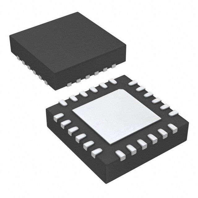
| 描述 | IC SUPERVISOR 4CH UV 24QFN监控电路 W/ANNEAL 4-CH UV SUPERVISOR Y IC |
| 产品分类 | |
| 品牌 | Intersil |
| 产品手册 | |
| 产品图片 |
|
| rohs | 符合RoHS无铅 / 符合限制有害物质指令(RoHS)规范要求 |
| 产品系列 | 电源管理 IC,监控电路,Intersil ISL6131IRZA- |
| NumberofInputsMonitored | 4 Input |
| 数据手册 | |
| 产品型号 | ISL6131IRZA |
| PCN设计/规格 | |
| 产品目录页面 | |
| 产品种类 | 监控电路 |
| 人工复位 | Manual Reset |
| 供应商器件封装 | 24-VQFN |
| 包装 | 管件 |
| 受监控电压数 | 4 |
| 商标 | Intersil |
| 复位 | 低有效 |
| 复位超时 | - |
| 安装类型 | 表面贴装 |
| 封装 | Tube |
| 封装/外壳 | 24-VFQFN 裸露焊盘 |
| 封装/箱体 | QFN-24 |
| 工作温度 | -40°C ~ 85°C |
| 工作电源电流 | 170 uA |
| 工厂包装数量 | 75 |
| 最大工作温度 | + 85 C |
| 最小工作温度 | - 40 C |
| 标准包装 | 75 |
| 欠电压阈值 | 0.7 V |
| 电压-阈值 | 可调节/可选择 |
| 电池备用开关 | No Backup |
| 电源电压-最大 | 5.5 V |
| 电源电压-最小 | 1.5 V |
| 监视器 | No Watchdog |
| 类型 | Voltage Supervisory |
| 系列 | ISL6131 |
| 被监测输入数 | 4 Input |
| 输出 | 开路漏极或开路集电极 |
| 输出类型 | Active Low |
| 阈值电压 | Adjustable |


- 商务部:美国ITC正式对集成电路等产品启动337调查
- 曝三星4nm工艺存在良率问题 高通将骁龙8 Gen1或转产台积电
- 太阳诱电将投资9.5亿元在常州建新厂生产MLCC 预计2023年完工
- 英特尔发布欧洲新工厂建设计划 深化IDM 2.0 战略
- 台积电先进制程称霸业界 有大客户加持明年业绩稳了
- 达到5530亿美元!SIA预计今年全球半导体销售额将创下新高
- 英特尔拟将自动驾驶子公司Mobileye上市 估值或超500亿美元
- 三星加码芯片和SET,合并消费电子和移动部门,撤换高东真等 CEO
- 三星电子宣布重大人事变动 还合并消费电子和移动部门
- 海关总署:前11个月进口集成电路产品价值2.52万亿元 增长14.8%


PDF Datasheet 数据手册内容提取
DATASHEET ISL6131, ISL6132 FN9119 Multiple Voltage Supervisory ICs Rev 6.00 February 11, 2014 The ISL6131 and ISL6132 are a family of high-accuracy, Features multi-voltage supervisory ICs designed to monitor voltages greater than 0.7V in applications ranging from • Operates from 1.5V to 5.5V Supply Voltage microprocessors to industrial power systems. The ISL6131 is • Four Adjustable Voltage Monitoring Thresholds an undervoltage four-supply supervisor, and the ISL6132 is a • 150ms STATUS/PGOOD Stability Time Delay two-voltage supervisor monitoring for undervoltage (UV) and • Four Individual Open Drain STATUS Outputs overvoltage (OV) conditions. • Guaranteed STATUS/PGOOD Valid to VDD <1V Both ICs feature four external resistor programmable voltage monitoring (VMON) inputs, each with a related STATUS output • VDD and VMON Glitch Immunity that individually reports the related monitor input condition. In • VDD Lock-Out addition, there is a Power-Good (PGOOD) signal that asserts • 4mm X 4mm QFN Package high when the STATUS outputs are in their correct state. A - Compliant to JEDEC PUB95 MO-220 stability delay of approximately 160ms ensures that the QFN - Quad Flat No Leads - Package Outline monitored supply is stable before STATUS and PGOOD are - Near Chip Scale Package footprint, which improves PCB released to go high. The PGOOD and STATUS outputs are efficiency and has a thinner profile open-drain to allow OR’ing of the signals and interfacing to a wide range of logic levels. • Pb-Free (RoHS Compliant) STATUS and PGOOD outputs are guaranteed to be valid with IC Applications bias lower than 1V, eliminating concern about STATUS and • Multivoltage DSPs and Processors PGOOD outputs during IC bias up and down. VMON inputs are designed to ignore momentary transients on the monitored • µP Voltage Monitoring supplies. • Embedded Control Systems • Graphics Cards • Intelligent Instruments • Medical Equipment • Network Routers • Portable Battery-Powered Equipment • Set-Top Boxes • Telecommunications Systems 1 1 2 2 _ _ _ _ S S S S U U U U D C B A AT AT AT AT N N ATUS ATUS ATUS ATUS D IN C IN B IN A IN UVST OVST UVST OVST V2 I V1 I T T T T Ru S S S S VDD VDD VMON_A UVMON_1 UVMON_2 Rm VMON_B GROUND GROUND OVMON_1 VMON_C VMON_D PGOOD1 OVMON_2 Rl PGOOD PGOOD2 EN1 EN2 EN FIGURE 1. ISL6131 TYPICAL APPLICATION USAGE FIGURE 2. ISL6132 TYPICAL APPLICATION USAGE FN9119 Rev 6.00 Page 1 of 15 February 11, 2014
ISL6131, ISL6132 Ordering Information Pin Configuration ISL6131, ISL6132 PART TEMP. (24 LD QFN) NUMBER PART RANGE PACKAGE PKG. TOP VIEW (Notes 2, 3) MARKING (°C) (Pb-free) DWG. # 24 23 22 21 20 19 ISL6131IRZA 61 31IRZ -40 to +85 24 Ld 4x4 QFN L24.4x4 (Note 1) 1 18 ISL6132IRZA 61 32IRZ -40 to +85 24 Ld 4x4 QFN L24.4x4 2 17 (Note 1) 3 16 ISL6131EVAL1Z Evaluation Board PD ISL6132EVAL1Z Evaluation Board 4 15 NOTES: 5 14 1. Add “-T*” suffix for tape and reel. Please refer to TB347 for details on 6 13 reel specifications. 2. These Intersil Pb-free plastic packaged products employ special 7 8 9 10 11 12 Pb-free material sets, molding compounds/die attach materials, and 100% matte tin plate plus anneal (e3 termination finish, which is RoHS compliant and compatible with both SnPb and Pb-free soldering operations). Intersil Pb-free products are MSL classified at Pb-free peak reflow temperatures that meet or exceed the Pb-free requirements of IPC/JEDEC J STD-020. 3. For Moisture Sensitivity Level (MSL), please see device information page for ISL6131, ISL6132. For more information on MSL, please see Tech Brief TB363. Pin Descriptions PIN 6131 6132 PIN NAME FUNCTION DESCRIPTION 23 23 VDD Bias IC from nominal 1.5V to 5V 10 10 GND IC ground 20 NA VMON_A On the ISL6131, these inputs provide a programmable UV threshold referenced to an internal 0.633V. The related STATUS output asserts when the related input > internal reference voltage. 12 NA VMON_B On the ISL6132, these inputs provide a programmable UV and OV threshold referenced to an internal 0.633V 17 NA VMON_C reference. In the ‘AB’ pair, VMON_A is the UV input, and VMON_B is the OV input. In the ‘CD’ pair, VMON_C is the UV input, and VMON_D is the OV input. 14 NA VMON_D These inputs have a 30µs glitch filter to prevent PGOOD reset caused by a transient. NA 12 OVMON_1 NA 20 UVMON_1 NA 17 UVMON_2 NA 14 OVMON_2 24 24 PGOOD On the ISL6131, PGOOD is the Boolean AND function of all four STATUS outputs. On the ISL6132, PGOOD is for the AB pair and signals high when the monitored voltage is within the specified window and the A and B STATUS output states are correct. This is an open-drain output and is to be pulled high to the appropriate level with an external resistor to a VDD maximum level. NA 9 PGOOD2 PGOOD2 is for the CD pair and signals high when the monitored voltage is within the specified window and when the C and D STATUS output states are correct. This is an open-drain output and is to be pulled high to the appropriate level with an external resistor to a VDD maximum level. FN9119 Rev 6.00 Page 2 of 15 February 11, 2014
ISL6131, ISL6132 Pin Descriptions (Continued) PIN 6131 6132 PIN NAME FUNCTION DESCRIPTION 2 NA STATUS_A On the ISL6131, each STATUS provides a high signal through pull-up resistors about 160ms after its related VMON has continuously been > Vuv_vth. This delay is for stabilization of monitored voltages. STATUS de-asserts and pulls 5 NA STATUS_B low upon VMON not being satisfied for about 30µs. 6 NA STATUS_C On the ISL6132, the STATUS outputs indicate compliance with a high output state for each pair of monitors. 7 NA STATUS_D NA 5 OVSTATUS_1 NA 2 UVSTATUS_1 NA 6 UVSTATUS_2 NA 7 OVSTATUS_2 1 1 EN1 On the ISL6131, this pin provides four voltage UV functions for enabling/disabling input. Internally pulled up to VDD. Controls monitor 1 (AB pair) on ISL6132. NA 11 EN2 On the ISL6132, this pin controls monitor 2 (CD pair) voltage and voltage monitoring function enabling input; pulled up to VDD. - - PD Thermal Pad. Should be electrically connected to GND. NC 3, 4, 8, 13, 15, 16, 18, No Connect 19, 21, 22 FN9119 Rev 6.00 Page 3 of 15 February 11, 2014
ISL6131, ISL6132 Absolute Maximum Ratings Thermal Information VDD. . . . . . . . . . . . . . . . . . . . . . . . . . . . . . . . . . . . . . . . . . . . . . . . . . . . . . +6.0V Thermal Resistance (Typical, Notes 4, 5) JA (°C/W) JC (°C/W) VMON, ENABLE, STATUS, PGOOD. . . . . . . . . . . . . . . . . . .-0.3V to VDD+0.3V 4x4 QFN Package. . . . . . . . . . . . . . . . . . . . . 48 9 ESD Classification. . . . . . . . . . . . . . . . . . . . . . . . . . . . . . . . . . . . . . 2kV (HBM) Maximum Junction Temperature . . . . . . . . . . . . . . . . . . . . . . . . . . . .+150°C Maximum Storage Temperature Range . . . . . . . . . . . . . .-65°C to +150°C Operating Conditions Pb-Free Reflow Profile . . . . . . . . . . . . . . . . . . . . . . . . . . . . . . . see link below http://www.intersil.com/pbfree/Pb-FreeReflow.asp VDD Supply Voltage Range . . . . . . . . . . . . . . . . . . . . . . . . . . .+1.5V to +5.5V Temperature Range (TA) . . . . . . . . . . . . . . . . . . . . . . . . . . . .-40°C to +85°C CAUTION: Do not operate at or near the maximum ratings listed for extended periods of time. Exposure to such conditions may adversely impact product reliability and result in failures not covered by warranty. NOTES: 4. JA is measured with the component mounted on a high effective thermal conductivity test board in free air. See Tech Brief TB379 for details. 5. For JC, the “case temp” location is the center of the exposed metal pad on the package underside. 6. All voltages are relative to GND, unless otherwise specified. Electrical Specifications Nominal VDD = 1.5V to +5V, TA = TJ = -40°C to +85°C, unless otherwise specified. Boldface limits apply over the operating temperature range, -40°C to +85°C. MIN MAX PARAMETER SYMBOL TEST CONDITIONS (Note 7) TYP (Note 7) UNIT VMON/ENABLE INPUTS VMON Falling Threshold VVMONvth TJ = +25°C 619 633 647 mV VMON Threshold Temp. Coeff. TCVMONvth TJ from -40°C to +85°C - 40 - V/°C VMON Hysteresis VVMONhys - 10 - mV VMON Glitch Filter Tfil - 30 - s VMON Minimum Input Impedance Zin_min TJ = +40°C, VMON within 63mV of VVMONvth 8 M ENABLE L2H, Delay to STATUS & PGOOD VMON valid, EN high to STATUS and PG high - 160 - ms EN H2L, Delay to PGOOD EN low to PGOOD low - - 0.1 s EN H2L, Delay to STATUS EN low to STATUS low - 13 - s ENABLE Pull-up Voltage EN open - VDD - V ENABLE Threshold Voltage VENVTH - VDD/2 - V STATUS/PGOOD OUTPUTS STATUS Pull-Down Current IRSTpd RST = 0.1V - 88 - mA STATUS/PGOOD Delay after VMON Valid TdelST VMON > VUVvth to STATUS = 0.2V - 160 - ms STATUS/PGOOD Output Low Vol Measured at VDD = 1.0V - 0.04 0.1 V BIAS IC Supply Current IVDD_5.5V VDD = 5V - 170 - A IC Supply Current IVDD_3.3V VDD = 3.3V - 145 - A IC Supply Current IVDD_1.5V VDD = 1.5V - 100 - A VDD Power On VDD_POR VDD high to low - 0.89 1 V VDD Power On Lock Out VDD_LO VDD low to high - 0.91 - V NOTE: 7. Parameters with MIN and/or MAX limits are 100% tested at +25°C, unless otherwise specified. Temperature limits established by characterization and are not production tested. FN9119 Rev 6.00 Page 4 of 15 February 11, 2014
ISL6131, ISL6132 Description and Operation input>VMON Vth continuously for ~160ms, its associated STATUS output releases high, indicating that the minimum The ISL6131 is a four-voltage, high-accuracy, supervisory IC voltage condition has been met. As both UVMON and OVMON designed to monitor multiple voltages greater than 0.7V relative inputs are satisfied, the PGOOD output is released to go high, to Pin 10 of the IC. indicating that the monitored voltage is within the specified window. Figure 18 shows this performance for a 4V to 5V Upon VDD bias power-up, the STATUS and PGOOD outputs are window. held correctly low once VDD is as low as 1V. Once biased to 1.5V, the IC continuously monitors from one to four voltages When VMON does not satisfy its voltage high or low criteria for independently through external resistor dividers, comparing each more than the glitch filter time, the associated STATUS and voltage monitoring (VMON) pin voltage to an internal 0.633V PGOOD are pulled low. Figures 19 and 20 show this performance (VVMONvth) reference. for a 4V to 5V compliant window. With the EN input driven high or open, as each VMON input rises Figures 21 through 23 show the VMON glitch filter timing to above VVMONvth, a timer is set to ensure ~160ms of continuous STATUS and PGOOD notification and transient immunity. compliance. Then the related STATUS output is released to be pulled high. The STATUS outputs are open-drain to allow OR’ing of The ENABLE input, when pulled low, allows the monitoring and these signals and interfacing to a logic high level up to VDD. The reporting functions to be disabled. Figure 24 shows ENABLE high STATUS outputs are designed to reject short transients (~30s) to PGOOD timing for compliant voltage. on the VMON inputs. Once all STATUS outputs are high, a When choosing resistors for the divider, remember to keep the Power-Good (PGOOD) output signal is generated high to indicate current through the string bounded by power loss tolerance at the that all monitored voltages are greater than minimum top end and noise immunity at the bottom end. For most compliance level. applications, total divider resistance in the 10k -100krange Once any VMON input falls below VVMONvth for longer than the is advisable, with 1% tolerance resistors being used to reduce glitch filter time, both the PGOOD and the related STATUS output monitoring error. are pulled low. The other STATUS outputs remain high as long as Figures 1 and 2 show that choosing the two resistor values is their corresponding VMON voltage remains valid and the PGOOD straightforward for the ISL6131, because the ratio of resistance validation process is reset. should equal the ratio of the desired trip voltage to the internal Figure 1 shows the ISL6131 typical application schematic, and reference, 0.633V. Figure 3 is an operational timing diagram. See Figures 10 to 17 for For the ISL6132, two dividers of two resistors each can be ISL6131 function and performance. Figures 10 and 11 show the employed to monitor the OV and UV levels for each voltage. VDD rising along with STATUS and PGOOD response. Figures 12 Otherwise, use a single three-resistor string for each voltage. In and 13 illustrate VMON falling below VVMONvth, and Figure 14 the three-resistor divider string, the ratio of the desired shows VMON rising above VVMONvth with STATUS and PGOOD overvoltage trip point to the internal reference is equal to the response. Figure 15 shows VDD failing, with STATUS and PGOOD ratio of the two upper resistors to the lowest (GND connected) response. Figures 16 and 17 show ENABLE to STATUS and PGOOD resistor. The desired undervoltage trip point ratio to the internal timing. reference voltage is equal to the ratio of the uppermost (voltage If less than four voltages are being monitored, connect the connected) resistor to the two lower resistors, as shown in the unused VMON pins to VDD for proper operation. All unused following example: STATUS outputs can be left open. 1. Establish lower and upper trip level: 3.3V ±20% or 2.64V (UV) The ISL6132 is a dual voltage monitor for undervoltage and and 3.96V (OV) overvoltage compliance. Figure 2 shows the typical ISL6132 2. Establish total resistor string value: 10kIr = divider current implementation schematic, and Figure 4 is the operational timing 3. (Rm + Rl) * Ir = 0.623V @ UV and Rl * Ir = 0.633V @ OV diagram. 4. Rm + Rl = 0.623V/Ir @ UV => Rm + Rl = There are two pairs of monitors, each with an undervoltage 0.623V/(2.64V/10kΩ) = 2.359kΩ (UVMON) input and an overvoltage (OVMON) input, along with 5. Rl = 0.633V/Ir @ OV => Rl = 0.633V/(3.96V/10kΩ) = 1.598kΩ associated STATUS and PGOOD outputs. 6. Rm = 2.359kΩ - 1.598kΩ = 0.761kΩ Upon VDD bias power-up, the STATUS and PGOOD outputs are 7. Ru = 10kΩ - 2.397kΩ = 7.641kΩ held correctly low, once VDD is as low as 1V. Once biased to 1.5V, Choose standard value resistors that most closely approximate the IC continuously monitors the voltage through external resistor these ideal values. Choosing a different total divider resistance dividers, comparing each VMON pin voltage to an internal 0.633V value may yield a more ideal ratio with available resistors values. reference. At proper bias, OVSTATUS is pulled high, and UVSTATUS and PGOOD are pulled low. Once the UVMON FN9119 Rev 6.00 Page 5 of 15 February 11, 2014
ISL6131, ISL6132 A B C D D C VMONVth VMON IVNOPLUTTAGE STSDLY STSDLY <Tfil >Tfil STSDLY STSDLY STSDLY C A B C D STATUS OUTPUTS PGOOD OUTPUT EN INPUT FIGURE 3. ISL6131 OPERATIONAL TIMING DIAGRAM OVERVOLTAGE OV LIMIT Tfil TdelST UNDERVOLTAGE <Tfil LIMIT TdelST Tfil MONITORED VOLTAGE RAMPING UP & DOWN OVSTATUS UVSTATUS PGOOD OUTPUT FIGURE 4. ISL6132 OPERATIONAL DIAGRAM Typical Performance Curves 634 0.30 633 VDD = 5V 0.25 V) 632 mA) D (m 631 NT ( 0.20 L E SHO 630 VDD = 1.5V URR 0.15 E C V THR 629 BIAS 0.1 U 628 B V 627 0.05 626 -40 -20 0 20 40 60 80 100 -40 -20 0 20 40 60 80 100 TEMPERATURE (°C) TEMPERATURE (°C) FIGURE 5. UV THRESHOLD FIGURE 6. VDD CURRENT FN9119 Rev 6.00 Page 6 of 15 February 11, 2014
ISL6131, ISL6132 Applications Usage Using the ISL6131EVAL1Z and ISL6132EVAL1Z Platforms VIN VOUT EN DC-DC_A The ISL6131EVAL1Z platform is set up to monitor and report an undervoltage condition on each of 12V, 5V, 3.3V and 1.2V VIN VOUT supplies to a -20% tolerance. EN DC-DC_B Each monitored supply has an individual STATUS output and an VIN AND’ed PGOOD output signal for all four supplies. An OFF LED is VOUT the PGOOD indicator for all four supplies. The ENABLE input EN DC-DC_C enables or disables the voltage monitoring function. See Figures 10 to 17 for performance and function examples. The ISL6132EVAL1Z platform is set up to monitor and report either an undervoltage or an overvoltage condition on 5V and 12V supplies to a ±10% tolerance. There is an OV and a UV ABC STATUS VMON_A STATUS output for each of the two supplies and individual AND’ed PGOOD outputs when each voltage is within the PGOOD VMON_D programmed voltage range. An OFF LED indicates compliance to ISL6131 VMON_C the voltage range upper and lower limits. VDD VMON_B The ENABLE inputs enable or disable the voltage monitoring ENABLE GND functions for each monitor supply. See Figures 18 to 24 for performance and function examples. Figures 25 and 26 illustrate the ISL6131EVAL1Z and FIGURE 7. ISL6131 “LOSSLESS” SEQUENCING CONFIGURATION ISL6132EVAL1Z platforms respectively in image and schematic. Using the ISL6131, ISL6132 for Negative Using the ISL6131 for System Voltage and Voltage Monitoring Applications Over-Temperature Monitoring The ISL6131, ISL6132 can be used for -V monitoring because it As a multi-voltage monitoring IC, the ISL6131 can monitor monitors any voltage that is more positive relative to its GND pin. over-temperature as well as voltage for more complete coverage With correct bias differential, these parts can monitor any of system stability. Using a Negative Temperature Coefficient voltage, regardless of polarity or amplitude. (NTC) passive device in place of one of the resistors in a VMON divider provides over-temperature monitoring either locally or Using the ISL6131 for “Lossless” Sequencing remotely. Applications Evaluations of this application configuration have involved the The ISL6131 can be used in a “lossless” sequencing application QT0805T-202J, QT0805Y-502J and QT0805Y-103J NTCs from in which a monitored output voltage determines the start of the Quality Thermistor. next sequenced turn-on. As shown in Figure 7, VMON_A input ISL6131 over-temperature monitoring is not as accurate as looks at the common VIN of several DC-DC converters and specific temperature monitor ICs, but this implementation enables DC-DC_A with STATUS _A, once both VIN and ENABLE are provides a cost-efficient solution with 5% tolerances achievable. satisfied. VMON_B monitors the output of DC-DC_A, and when the acceptable output voltage is reached, DC-DC_B is enabled See Figures 8 and 9 for over-temperature sensing configuration with STATUS_B output. This sequencing pattern continues until and operation results. In this example, the desired maximum all DC-DC outputs are on, at which time PGOOD signal is temperature is 100°C. The QT0805Y-103J NTC was placed at the released. A delay of 160ms from VMON > VVMONVth to STATUS end of 3 feet of twisted pair wire to emulate a remote sensing high ensures stability at each step prior to subsequent turn-on. application. According to the Quality Thermistor data sheet, this Additional ISL6131s can be employed in parallel to sequence any NTC device has a +25°C value of 10K and a +100°C value of number of DC-DC convertors in this fashion. 0.923K. An accompanying standard value resistor of 3.83K was chosen for the divider so that at 100°C, VMON ~0.633V with the bias voltage at 3.3V. The resulting falling VMON trip point with the configuration shown is ~0.634V, with ~0.642V for rising, which equates to ~95°C for under-temperature and ~97°C for over-temperature, respectively. Choosing the standard resistor value above and below R1 allows for small adjustments in the temperature trip point. FN9119 Rev 6.00 Page 7 of 15 February 11, 2014
ISL6131, ISL6132 The low ISL6131 VMON temperature coefficient makes it a TEMP (°C) VMON (V) TEMP STATUS viable and low-cost addition to complete system monitoring. 25 2.36 H = Under Temp TEMP INDICATOR 50 1.61 H = Under Temp STATUS 75 1.01 H = Under Temp 3.3V VDD 95 0.67 H = Under Temp 3.83k 100 0.61 L = Over Temp R1 105 0.54 L = Over Temp VMON T ISL6131 VMON 0.1V/DIV QT0805Y-103J (REMOTE HEAT GND SOURCE LOCATION) FIGURE 8. ISL6131 OVER-TEMP SENSING CONFIGURATION LOW = OVER TEMP TEMP STATUS 5V/DIV 10s/DIV FIGURE 9. ISL6132 OVER-TEMP SENSING RESULT FN9119 Rev 6.00 Page 8 of 15 February 11, 2014
ISL6131, ISL6132 Functional and Performance Waveforms VDD RISING STATUS OUTPUTS PULLED UP TO 1.5V STATUS OUTPUTS TO VDD VDD RISING PGOOD PGOOD 1V/DIV 100s/DIV 1V/DIV 200s/DIV FIGURE 10. ISL6131 VDD RISING FIGURE 11. ISL6131 VDD RISING WITH PULL-UP VMON FALLING BELOW UV Vth (0.1V/DIV) VMON FALLING BELOW UV Vth (0.1V/DIV) UV Vth 0.63V UV Vth 0.63V UNRELATED STATUS OUTPUTS UNRELATED STATUS OUTPUTS RELATED STATUS OUTPUT RELATED STATUS OUTPUT PGOOD PGOOD 1V/DIV 40ms/DIV 1V/DIV 10ms/DIV FIGURE 12. ISL6131 VMON FALLING TO PGOOD FIGURE 13. ISL6131 VMON FALLING TO PGOOD VMON RISING ABOVE UV Vth (0.1V/DIV) UV Vth 0.63V VDD FALLING UNRELATED STATUS OUTPUTS STATUS OUTPUTS RELATED STATUS OUTPUT PGOOD PGOOD 1V/DIV 20ms/DIV 1V/DIV 40ms/DIV FIGURE 14. ISL6131 UV RISING TO PGOOD FIGURE 15. ISL6131 VDD FALLING FN9119 Rev 6.00 Page 9 of 15 February 11, 2014
ISL6131, ISL6132 Functional and Performance Waveforms (Continued) ENABLE STATUS ENABLE STATUS PGOOD PGOOD 2V/DIV 20ms/DIV 2V/DIV 2µs/DIV FIGURE 16. ISL6131 ENABLE L2H TO PGOOD FIGURE 17. ISL6131 EN H2L TO PGOOD MONITORING 4V TO 5V MONITORING 4V TO 5V OV STATUS VDD RISING MONITORED VOLTAGE FALLING UV/PGOOD STATUS RISING OV STATUS RISING PGOOD AND UV STATUS PULLED LOW 1V/DIV 40ms/DIV 1V/DIV 10ms/DIV FIGURE 18. ISL6132 TURN-ON FIGURE 19. ISL6132 IN UV CONDITION MONITORING 4V TO 5V MONITORING 4V TO 5V UV STATUS VMON FALLING (1V/DIV) MONITORED VOLTAGE RISING 4V MIN LIMIT UV STATUS PGOOD AND OV STATUS PULLED LOW OV STATUS PGOOD 1V/DIV 10ms/DIV 5V/DIV 10µs/DIV FIGURE 20. ISL6132 IN OV CONDITION FIGURE 21. ISL6132 UV GLITCH FILTER TIMING FN9119 Rev 6.00 Page 10 of 15 February 11, 2014
ISL6131, ISL6132 Functional and Performance Waveforms (Continued) MONITORING 4V TO 5V VMON RISING (1V/DIV) 5V MAX LIMIT VMON 5.5V TO 3.5V UV STATUS UV, OV STATUS & PGOOD OV STATUS 5VOUT PGOOD 5V/DIV 10µs/DIV 8µs/DIV FIGURE 22. ISL6132 OV GLITCH FILTER TIMING FIGURE 23. ISL6132 GLITCH FILTER TRANSIENT IMMUNITY ENABLE PGOOD OV, UV STATUS 1V/DIV 20ms/DIV FIGURE 24. ISL6132 ENABLE TO PGOOD FN9119 Rev 6.00 Page 11 of 15 February 11, 2014
ISL6131, ISL6132 ISL6131EVAL1Z and ISL6132EVAL1Z Descriptions 5V R12 R11 1.2V 10k 10k 5V STATUS 12V STATUS 3.3V R10 R9 12V 10k 10k 1.2V STATUS 3.3V STATUS 2 5 6 7 A B C D STATUS R4 R2 R3 R1 23 VDD 53.6k 5.11k 31.6k140k 12 C1 VMONB 1µF 14 VMOND R13 R8 17 5.11k 10k 1R06k VMONC ISL6131 D1 R7 20 10k VMONA R5 24 10k PGOOD PGOOD EP GND 1 10 EN1 FIGURE 25. ISL6131EVAL1Z SCHEMATIC AND PHOTOGRAPH FN9119 Rev 6.00 Page 12 of 15 February 11, 2014
ISL6131, ISL6132 5V R12 R11 10k 10k 5V OV STATUS 5V UV STATUS R9 R10 10k 12V 10k 12V OV STATUS 12V UV STATUS 2 5 6 7 UV1 OV1 UV2 OV2 STATUS 23 VDD R4 R3 R2 R1 76.8k 61.9k196k 158k 12 C1 OVMON1 1µF 20 UVMON1 R13 R14 R8 14 10k 10k 10k R7 OVMON2 10k R6 17 ISL6132 D1 D2 UVMON2 10k 24 R5 PGOOD 5V PGOOD 10k 9 PGOOD2 12V PGOOD EP GND 1 11 10 EN1 EN2 FIGURE 26. ISL6132EVAL1Z SCHEMATIC AND PHOTOGRAPH TABLE 1. ISL6131EVAL1Z, ISL6132EVAL1Z COMPONENT LISTING COMPONENT DESIGNATOR COMPONENT FUNCTION COMPONENT DESCRIPTION U1 ISL6131, Quad Undervoltage Supervisor Intersil, ISL6131IR Quad Undervoltage Supervisor R1 12V Upper Divider Resistor 140kΩ R2 1.2V Upper Divider Resistor 5.11kΩ R3 3.3V Upper Divider Resistor 31.6kΩ R4 5V Upper Divider Resistor 53.6kΩ U1 ISL6132, Dual Over & Undervoltage Supervisor Intersil, ISL6132IR Dual Overvoltage & Undervoltage Supervisor R1 12V Upper UV Divider Resistor 158kΩ R2 12V Upper OV Divider Resistor 196kΩ R3 5V Upper UV Divider Resistor 61.9kΩ R4 5V Upper OV Divider Resistor 76.8kΩ R5, R6, R7, R8 Lower Divider Resistors 10kΩ R9, R10, R11, R12 STATUS Pull-up Resistors 10kΩ C1 Decoupling Capacitor 1µF D1, D2 PGOOD# INDICATOR SMD RED LED FN9119 Rev 6.00 Page 13 of 15 February 11, 2014
ISL6131, ISL6132 Revision History The revision history provided is for informational purposes only and is believed to be accurate, but not warranted. Please go to web to make sure you have the latest revision. DATE REVISION CHANGE February 11, 2014 FN9119.6 • On page5 - right hand column, paragraph 5 that starts with: "For the ISL6131, two dividers of two resistors each can be employed to monitor the OV and UV levels for each voltage. Otherwise, use a single three-resistor string for each voltage." Changed ISL6131 to ISL6132. • On page 14 - Updated Products section to updated About Intersil verbiage July 18, 2011 FN9119.5 • On page2, Ordering Information: added ISL6131EVAL1Z and ISL6132EVAL1Z Evaluation Boards. • On page7: changed "Using the ISL613XSUPEREVAL2 Platform" section to "Using the ISL6131EVAL1Z and ISL6132EVAL1Z Platforms" and rewrote text. • On page12: replaced Fig. 25, “ISL613XSUPEREVAL2 PHOTOGRAPH” with “ISL6131EVAL1Z SCHEMATIC AND PHOTOGRAPH.“ • On page13: replaced Fig. 26, “ISL613XSUPEREVAL2 CHANNEL 1 SCHEMATIC” with “ISL6132EVAL1Z SCHEMATIC AND PHOTOGRAPH.” • Converted to latest datasheet template. August 17, 2010 FN9119.4 • P1: Removed prenotification part ISL6132IR & Obsolete part ISL6131IR from Order Info. Added Part Marking column to Order Info. Updated Pb-free bullet in Features and Pb-free note in Ordering Information based on lead finish. Added TB347 link to ordering information for reel specifications. • P3: Per customer request, added "PD" label to Pinout and description to Pin Descriptions table, which states "Thermal Pad. Should be electrically connected to GND". • P4: Updated Caution statement in Abs Max. Removed Max Lead Soldering Temp from Thermal Info and replaced with Pb-Free Reflow link. Added standard temp range note to spec table MIN MAX columns. • P13: Updated POD to latest released. Changes were to convert to new QFN format and correct Note 4 (corrected “0.015mm and 0.30mm” to “0.15mm and 0.30mm”). July 22, 2005 FN9119.3 • Added additional application usage text to clarify component choice. Corrected typographical errors in spec table. August 18, 2004 FN9119.2 • Added Pb-free parts. March 5, 2004 FN9119.1 • Added application information. July 15, 2003 FN9119.0 Initial Release About Intersil Intersil Corporation is a leader in the design and manufacture of high-performance analog, mixed-signal and power management semiconductors. The company's products address some of the largest markets within the industrial and infrastructure, personal computing and high-end consumer markets. For more information about Intersil, visit our website at www.intersil.com. For the most updated datasheet, application notes, related documentation and related parts, please see the respective product information page found at www.intersil.com. You may report errors or suggestions for improving this datasheet by visiting www.intersil.com/en/support/ask-an-expert.html. Reliability reports are also available from our website at http://www.intersil.com/en/support/qualandreliability.html#reliability © Copyright Intersil Americas LLC 2003-2014. All Rights Reserved. All trademarks and registered trademarks are the property of their respective owners. For additional products, see www.intersil.com/en/products.html Intersil products are manufactured, assembled and tested utilizing ISO9001 quality systems as noted in the quality certifications found at www.intersil.com/en/support/qualandreliability.html Intersil products are sold by description only. Intersil may modify the circuit design and/or specifications of products at any time without notice, provided that such modification does not, in Intersil's sole judgment, affect the form, fit or function of the product. Accordingly, the reader is cautioned to verify that datasheets are current before placing orders. Information furnished by Intersil is believed to be accurate and reliable. However, no responsibility is assumed by Intersil or its subsidiaries for its use; nor for any infringements of patents or other rights of third parties which may result from its use. No license is granted by implication or otherwise under any patent or patent rights of Intersil or its subsidiaries. For information regarding Intersil Corporation and its products, see www.intersil.com FN9119 Rev 6.00 Page 14 of 15 February 11, 2014
ISL6131, ISL6132 Package Outline Drawing L24.4x4 24 LEAD QUAD FLAT NO-LEAD PLASTIC PACKAGE Rev 4, 10/06 4X 2.5 4.00 A 20X 0.50 B PIN #1 CORNER 19 24 (C 0 . 25) PIN 1 INDEX AREA 18 1 00 2 . 10 ± 0 . 15 4. 13 (4X) 0.15 12 7 TOP VIEW 24X 0 . 4 ± 0 . 1 0.10 M C A B 24X 0 . 23 +- 00 .. 0057 4 BOTTOM VIEW SEE DETAIL "X" 0.10 C 0 . 90 ± 0 . 1 C BASE PLANE ( 3 . 8 TYP ) SEATING PLANE SIDE VIEW 0.08 C ( 2 . 10 ) ( 20X 0 . 5 ) C 0 . 2 REF 5 ( 24X 0 . 25 ) 0 . 00 MIN. ( 24X 0 . 6 ) 0 . 05 MAX. DETAIL "X" TYPICAL RECOMMENDED LAND PATTERN NOTES: 1. Dimensions are in millimeters. Dimensions in ( ) for Reference Only. 2. Dimensioning and tolerancing conform to AMSE Y14.5m-1994. 3. Unless otherwise specified, tolerance : Decimal ± 0.05 4. Dimension b applies to the metallized terminal and is measured between 0.15mm and 0.30mm from the terminal tip. 5. Tiebar shown (if present) is a non-functional feature. 6. The configuration of the pin #1 identifier is optional, but must be located within the zone indicated. The pin #1 indentifier may be either a mold or mark feature. FN9119 Rev 6.00 Page 15 of 15 February 11, 2014