ICGOO在线商城 > 射频/IF 和 RFID > RF 放大器 > ISL55012IEZ-T7
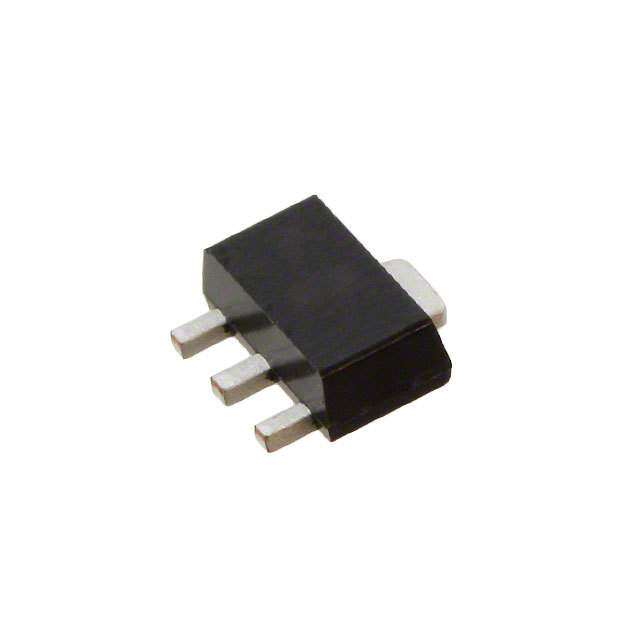
- 型号: ISL55012IEZ-T7
- 制造商: Intersil
- 库位|库存: xxxx|xxxx
- 要求:
| 数量阶梯 | 香港交货 | 国内含税 |
| +xxxx | $xxxx | ¥xxxx |
查看当月历史价格
查看今年历史价格
ISL55012IEZ-T7产品简介:
ICGOO电子元器件商城为您提供ISL55012IEZ-T7由Intersil设计生产,在icgoo商城现货销售,并且可以通过原厂、代理商等渠道进行代购。 ISL55012IEZ-T7价格参考¥5.31-¥12.03。IntersilISL55012IEZ-T7封装/规格:RF 放大器, 射频放大器 IC 蓝牙 500MHz ~ 3GHz SC-70-6。您可以下载ISL55012IEZ-T7参考资料、Datasheet数据手册功能说明书,资料中有ISL55012IEZ-T7 详细功能的应用电路图电压和使用方法及教程。
ISL55012IEZ-T7 是由 Renesas Electronics America Inc. 生产的一款 RF 放大器。该器件具有卓越的性能和可靠性,适用于多种无线通信和射频应用领域。

 应用场景

1. 无线通信基础设施:
   - 基站:ISL55012IEZ-T7 可用于蜂窝基站中的射频信号放大,确保信号传输的稳定性和覆盖范围。其低噪声和高线性度特性使其在多载波环境下表现出色。
   - 中继站:在中继站中,该放大器可以增强远距离传输的信号强度,减少信号衰减,提高通信质量。

2. 无线局域网 (WLAN):
   - 路由器和接入点:在 Wi-Fi 路由器和接入点中,ISL55012IEZ-T7 可以提升信号的发射功率和接收灵敏度,从而扩大网络覆盖范围并提高数据传输速率。

3. 卫星通信:
   - 地面站设备:在卫星通信系统的地面站设备中,该放大器可以用于信号的上行和下行链路放大,确保与卫星之间的高效通信。
   - 便携式终端:在便携式卫星通信终端中,ISL55012IEZ-T7 的小型化设计和低功耗特性使其成为理想选择。

4. 雷达系统:
   - 气象雷达:在气象雷达中,该放大器可以增强回波信号的强度,提高探测精度和距离。
   - 军事雷达:在军事雷达系统中,ISL55012IEZ-T7 的高可靠性和抗干扰能力使其能够在复杂电磁环境中稳定工作。

5. 物联网 (IoT) 设备:
   - 智能传感器:在物联网设备中,如智能家居、工业自动化等领域的智能传感器,ISL55012IEZ-T7 可以提供稳定的射频信号放大,确保数据的可靠传输。
   - 远程监控设备:在远程监控设备中,该放大器可以增强信号传输的稳定性,保证监控数据的实时性和准确性。

6. 医疗设备:
   - 无线医疗监测设备:在无线医疗监测设备中,如可穿戴健康监测设备,ISL55012IEZ-T7 可以确保患者数据的准确传输,支持远程医疗诊断。

总之,ISL55012IEZ-T7 凭借其优异的射频性能和可靠性,广泛应用于各种需要高性能射频放大的领域,满足了不同行业对高质量通信的需求。
| 参数 | 数值 |
| 产品目录 | |
| 描述 | IC AMP MMIC BIPO BROADBND SC70-6 |
| 产品分类 | |
| 品牌 | Intersil |
| 数据手册 | |
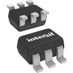
| 产品图片 |
|
| P1dB | 17.7dBm |
| 产品型号 | ISL55012IEZ-T7 |
| RF类型 | 蓝牙 |
| rohs | 无铅 / 符合限制有害物质指令(RoHS)规范要求 |
| 产品系列 | - |
| 供应商器件封装 | SC-70-6 |
| 其它名称 | ISL55012IEZ-T7CT |
| 包装 | 剪切带 (CT) |
| 噪声系数 | 4.7dB |
| 增益 | 18.3dB |
| 封装/外壳 | 6-TSSOP,SC-88,SOT-363 |
| 标准包装 | 1 |
| 测试频率 | 1GHz |
| 电压-电源 | 3 V ~ 5.5 V |
| 电流-电源 | 63.5mA |
| 频率 | 500MHz ~ 3GHz |





- 商务部:美国ITC正式对集成电路等产品启动337调查
- 曝三星4nm工艺存在良率问题 高通将骁龙8 Gen1或转产台积电
- 太阳诱电将投资9.5亿元在常州建新厂生产MLCC 预计2023年完工
- 英特尔发布欧洲新工厂建设计划 深化IDM 2.0 战略
- 台积电先进制程称霸业界 有大客户加持明年业绩稳了
- 达到5530亿美元!SIA预计今年全球半导体销售额将创下新高
- 英特尔拟将自动驾驶子公司Mobileye上市 估值或超500亿美元
- 三星加码芯片和SET,合并消费电子和移动部门,撤换高东真等 CEO
- 三星电子宣布重大人事变动 还合并消费电子和移动部门
- 海关总署:前11个月进口集成电路产品价值2.52万亿元 增长14.8%




PDF Datasheet 数据手册内容提取
DATASHEET ISL55012 FN6258 MMIC Silicon Bipolar Broadband Amplifier Rev.3.00 Jul 20, 2017 The ISL55012 is a high performance gain block featuring a Features Darlington configuration using high fT transistors and excellent thermal performance. They are an ideal choice for DVB-S LNB • Input impedance of 75Ω cable receiver applications. • Output impedance of 50Ω Other members of the family include: • Gain of 18dB at 1GHz • ISL55012 and ISL55015 match a 75Ω source to a 50Ω load. • Noise figure of 4.7dB at 2GHz ISL55014 matches a 50Ω source to a 50Ω load. • OIP3 of 30dBm at 1GHz • Low input and output return losses Ordering Information • Pb-Free (RoHS compliant) PART TAPE AND PACKAGE Applications PART # MARKING REEL (RoHS PKG. (Notes1, 2, 3) (Note4) (UNITS) COMPLIANT) DWG. # • LNB and LNB-T (HDTV) amplifiers ISL55012IEZ-T7 CCG 3k 6 Ld SC-70 P6.049B • IF gain blocks for satellite and terrestrial STBs ISL55012IEZ-EVAL Evaluation Board • PA driver amplifier NOTES: • Wireless data, satellite 1. Refer to TB347 for details on reel specifications. • Bluetooth/WiFi 2. These Intersil Pb-free plastic packaged products employ special • Satellite locator and signal strength meters Pb-free material sets, molding compounds/die attach materials, and 100% matte tin plate plus anneal (e3 termination finish, which Pin Configuration is RoHS compliant and compatible with both SnPb and Pb-free soldering operations). Intersil Pb-free products are MSL classified at ISL55012 Pb-free peak reflow temperatures that meet or exceed the Pb-free (6 LD SC-70) requirements of IPC/JEDEC J STD-020. TOP VIEW 3. For Moisture Sensitivity Level (MSL), see product information page for ISL55012. For more information on MSL, see tech brief TB363. GND 1 6 OUT 4. The part marking is located on the bottom of the part. GND 2 5 GND Related Literature IN 3 4 VSP • For a full list of related documents, visit our website - ISL55012 product page +5V TABLE 1. KEY DIFFERENCES BETWEEN FAMILY OF PARTS IMPEDANCE GAIN NOISE FIGURE 24Ω SOURCE LOAD AT 1GHz AT 2GHz 0.1µF 100pF 100pF 0.1µF PART # (Ω) (Ω) (dB) (dB) ISL55012 75 50 18 4.7 100nH 4 3 ISL55014 50 50 17.2 4.3 68pF 6 68pF ISL55015 75 50 13.5 4.8 1, 2, 5 FIGURE 1. TYPICAL APPLICATION CIRCUIT FN6258 Rev.3.00 Page 1 of 7 Jul 20, 2017
ISL55012 Absolute Maximum Ratings Thermal Information (TA = +25°C) Supply Voltage from VSP to GND . . . . . . . . . . . . . . . . . . . . . . . . . . . . . . . . 6V Thermal Resistance (Typical) JA (°C/W) JC (°C/W) Input Voltage. . . . . . . . . . . . . . . . . . . . . . . . . . . . . . .VS+ +0.3V to GND -0.3V 6 Ld SC-70 (Notes5, 6) . . . . . . . . . . . . . . . . 255 195 ESD Rating Storage Temperature. . . . . . . . . . . . . . . . . . . . . . . . . . . . . .-65°C to +125°C Human Body Model (Per MIL-STD-883 Method 3015.7). . . . . . . .6000V Operating Junction Temperature . . . . . . . . . . . . . . . . . . . . . . . . . . . .+135°C Machine Model (Per EIAJ ED-4701 Method C-111) . . . . . . . . . . . . .300V Pb-Free Reflow Profile . . . . . . . . . . . . . . . . . . . . . . . . . . . . . . . . . . see TB493 Storage Temperature. . . . . . . . . . . . . . . . . . . . . . . . . . . . . .-65°C to +125°C Operating Junction Temperature . . . . . . . . . . . . . . . . . . . . . . . . . . . .+135°C Recommended Operating Conditions Ambient Operating Temperature . . . . . . . . . . . . . . . . . . . . .-40°C to +85°C CAUTION: Do not operate at or near the maximum ratings listed for extended periods of time. Exposure to such conditions may adversely impact product reliability and result in failures not covered by warranty.. NOTES: 5. JA is measured with the component mounted on a high-effective thermal conductivity test board in free air. See Tech Brief TB379 for details. 6. For JC, the “case temp” location is taken at the package top center. Electrical Specifications VSP = +5V, ZRSC = ZLOAD = 50Ω, TA = +25°C, 24Ω VSP to OUT, unless otherwise specified. MIN MAX PARAMETER SYMBOL TEST CONDITIONS (Note7) TYP (Note7) UNIT Supply Voltage VSP To operate below 5V, the 24Ω resistor to supply 3.0 5.5 V should be reduced Small Signal Gain Gt 1.0GHz 17 18.3 19.5 dB 1.5GHz 16.1 17.4 18.6 dB 2.0GHz 15.1 16.6 17.6 dB Output Power at 1dB Compression P1dB 1.0GHz 16 17.7 19 dBm 2.0GHz 15.9 17.2 18.9 dBm Output Third Order Intercept Point OIP3 1.0GHz 30 dBm 2.0GHz 27 dBm Output Second Order Intercept Point OIP2 Input tones at 1.0GHz and 1.1GHz, 44.2 dBm at input power = -15dBm, output tone 2.1GHz 3dB Bandwidth BW 3dB below gain at 500MHz 2.4 GHz Input Return Loss IRL 1.0GHz ZRSC = 75Ω, ZLOAD = 50Ω 23.5 dB Output Return Loss ORL 1.0GHz ZRSC = 75Ω ZLOAD = 50Ω 21.8 dB Reverse Isolation RISOL 2.0GHz 22.4 dB Noise Figure NF 2.0GHz 4.7 dB Device Operating Current ID 56 63.5 71 mA NOTE: 7. Parameters with MIN and/or MAX limits are 100% tested at +25°C, unless otherwise specified. Temperature limits established by characterization and are not production tested. FN6258 Rev.3.00 Page 2 of 7 Jul 20, 2017
ISL55012 Device Test Setup AGILENT _8753ES VNA 50Ω 50Ω CONNECTORLESS PICOSECOND LABS PLATFORM MODEL 5542 50Ω PIN 3 PIN 6 50Ω DC BLOCK DUT BIAS TEE PICOSECOND LABS MODEL 5508-110 5V 24Ω I1 I2 IDEVICE INPUT OUTPUT REFERENCE REFERENCE 5V PLANE PLANE POWER SUPPLY FIGURE 2. DEVICE TEST SETUP Typical Performance Curves ZSRC = 75Ω, ZLOAD = 50Ω 32 24 28 20 24 dB) 20 B) 16 RL ( 16 L (d 12 I R 12 O 8 8 4 4 0 0 0.5 1.0 1.5 2.0 2.5 3.0 0.5 1.0 1.5 2.0 2.5 3.0 FREQUENCY (GHz) FREQUENCY (GHz) FIGURE 3. INPUT RETURN LOSS vs FREQUENCY FIGURE 4. OUTPUT RETURN LOSS vs FREQUENCY Typical Performance Curves 50Ω environment 20 0 -2 18 -4 S21 (dB) 1146 S11 (dB) -1--086 -12 12 -14 10 -16 0.5 1.0 1.5 2.0 2.5 3.0 0.5 1.0 1.5 2.0 2.5 3.0 FREQUENCY (GHz) FREQUENCY (GHz) FIGURE 5. |S21| vs FREQUENCY FIGURE 6. |S11| vs FREQUENCY FN6258 Rev.3.00 Page 3 of 7 Jul 20, 2017
ISL55012 Typical Performance Curves 50Ω environment (Continued) -18 -8 -10 -12 -20 -14 S12 (dB) S22 (dB) --1186 -22 -20 -22 -24 -24 0.5 1.0 1.5 2.0 2.5 3.0 0.5 1.0 1.5 2.0 2.5 3.0 FREQUENCY (GHz) FREQUENCY (GHz) FIGURE 7. |S12| vs FREQUENCY FIGURE 8. |S22| vs FREQUENCY 34 20 FUNDAMENTAL 32 10 (1GHz) 0 30 FUNDAMENTAL -10 m) m) (1.1GHz) P3 (dB 2268 D (dB --3200 OI H -40 24 -50 IM2 (2.1GHz) 22 -60 20 -70 0.5 1.0 1.5 2.0 2.5 3.0 -25 -20 -15 -10 -5 0 FREQUENCY (GHz) INPUT POWER (dBm) FIGURE 9. OIP3 vs FREQUENCY FIGURE 10. IM2 vs INPUT POWER 7 20 N 19 6 O SI 18 E (dB) 5 PRESm) 17 R 4 MB 16 U Od OISE FIG 23 UTPUT CPOINT ( 111345 N O B 12 1 d 1 11 0 10 0.5 1.0 1.5 2.0 2.5 3.0 0.5 1.0 1.5 2.0 2.5 3.0 FREQUENCY (GHz) FREQUENCY (GHz) FIGURE 11. NOISE FIGURE vs FREQUENCY FIGURE 12. P1dB vs FREQUENCY FN6258 Rev.3.00 Page 4 of 7 Jul 20, 2017
ISL55012 Typical Performance Curves 50Ω environment (Continued) 7.0 8.0 9.0 1.0 1.2 1.4 1.6 6.0 0.2 1.8 5.0 2.0 0.4 4.0 0.6 3.0 3.0 0.8 4.0 1.0 2.0 0.1 5.0 8.0 6.0 7.0 6.0 8.0 9.100 1.0 4.0 S22 2.0 20 0 0.1 0.2 0.3 0.4 0.5 0.6 0.7 0.8 0.9 1.0 1.2 1.4 1.601.8.52.0GHz 3.0 4.0 5.0 10 20 5050 0.5GHz 1.0 05 0.2 3GHz 20 S 0.1 1.00.4 11 2.2 0.091 0.6 2.2 0.8 0.7 0.8 0.6 0.2 1.0 0.5 3G0.1Hz 8.0 0.4 0.3 6.0 0.3 0.4 4.0 0.5 0.2 0.6 2.0 8.1 0.7 0.8 0.9 1.0 2.1 4.1 6.1 RF Café 2002 FIGURE 13. S11 AND S22 vs FREQUENCY FN6258 Rev.3.00 Page 5 of 7 Jul 20, 2017
ISL55012 Revision History The revision history provided is for informational purposes only and is believed to be accurate, but not warranted. Please visit our website to make sure you have the latest revision. DATE REVISION CHANGE July 20, 2017 FN6258.3 Removed mention of obsolete part ISL55013. On page1: Updated Ordering Information table - added column for tape & reel quantity and added MSL note. Added Related Literature Thermal Resistance on page2: Updated JA from: 200 to: JA 255 and added JC 195. Updated corresponding Note5 and added Note6. Moved Storage Temperature and Operating Junction Temperature from Abs Max to Thermal Information section. Added Recommended Operating Conditions section and moved Ambient Operating Temperature to this section from Abs Max Added Revision History and About Intersil sections. Changed POD on page7 from P6.049A to P6.049B. About Intersil Intersil Corporation is a leading provider of innovative power management and precision analog solutions. The company's products address some of the largest markets within the industrial and infrastructure, mobile computing, and high-end consumer markets. For the most updated datasheet, application notes, related documentation, and related parts, see the respective product information page found at www.intersil.com. For a listing of definitions and abbreviations of common terms used in our documents, visit: www.intersil.com/glossary. You may report errors or suggestions for improving this datasheet by visiting www.intersil.com/ask. Reliability reports are also available from our website at www.intersil.com/support. © Copyright Intersil Americas LLC 2009-2017. All Rights Reserved. All trademarks and registered trademarks are the property of their respective owners. For additional products, see www.intersil.com/en/products.html Intersil products are manufactured, assembled and tested utilizing ISO9001 quality systems as noted in the quality certifications found at www.intersil.com/en/support/qualandreliability.html Intersil products are sold by description only. Intersil may modify the circuit design and/or specifications of products at any time without notice, provided that such modification does not, in Intersil's sole judgment, affect the form, fit or function of the product. Accordingly, the reader is cautioned to verify that datasheets are current before placing orders. Information furnished by Intersil is believed to be accurate and reliable. However, no responsibility is assumed by Intersil or its subsidiaries for its use; nor for any infringements of patents or other rights of third parties which may result from its use. No license is granted by implication or otherwise under any patent or patent rights of Intersil or its subsidiaries. For information regarding Intersil Corporation and its products, see www.intersil.com FN6258 Rev.3.00 Page 6 of 7 Jul 20, 2017
ISL55012 Small Outline Transistor Plastic Packages (SC70-6) P6.049B 0.20 (0.008) M C VIEW C 6 LEAD SMALL OUTLINE TRANSISTOR PLASTIC PACKAGE CL MILLIMETERS b e SYMBOL MIN MAX NOTES A 0.80 1.00 - 6 5 4 A1 0.000 0.09 - CL E1 CL E A2 0.80 0.91 - b 0.15 0.30 - 1 2 3 b1 0.15 0.25 - c 0.08 0.25 6 e1 C c1 0.10 0.15 6 D D 1.85 2.25 3 CL E 2.30 BSC - E1 1.15 1.35 3 SEATING e 0.65 Ref - A A2 A1 PLANE e1 1.30 Ref - -C- L 0.21 0.44 4 N 6 5 0.10 (0.004) C Rev. 0 4/07 NOTES: WITH b 1. Dimensioning and tolerance per ASME Y14.5M-1994. PLATING b1 2. Package conforms to EIAJ SC70 and JEDEC MO203AB. 3. Dimensions D and E1 are exclusive of mold flash, protrusions, c c1 or gate burrs. 4. Footlength L measured at reference to gauge plane. BASE METAL 5. “N” is the number of terminal positions. 6. These Dimensions apply to the flat section of the lead between 0.08mm and 0.15mm from the lead tip. For the most recent package outline drawing, see P6.049B. SEATING L PLANE C VIEW C FN6258 Rev.3.00 Page 7 of 7 Jul 20, 2017
 Datasheet下载
