ICGOO在线商城 > 集成电路(IC) > 接口 - 信号缓冲器,中继器,分配器 > ISL33001IUZ

 Datasheet下载
- 型号: ISL33001IUZ
- 制造商: Intersil
- 库位|库存: xxxx|xxxx
- 要求:
| 数量阶梯 | 香港交货 | 国内含税 |
| +xxxx | $xxxx | ¥xxxx |
查看当月历史价格
查看今年历史价格
ISL33001IUZ产品简介:
ICGOO电子元器件商城为您提供ISL33001IUZ由Intersil设计生产,在icgoo商城现货销售,并且可以通过原厂、代理商等渠道进行代购。 ISL33001IUZ价格参考。IntersilISL33001IUZ封装/规格:接口 - 信号缓冲器,中继器,分配器, Buffer, Accelerator 2 Channel 8-MSOP。您可以下载ISL33001IUZ参考资料、Datasheet数据手册功能说明书,资料中有ISL33001IUZ 详细功能的应用电路图电压和使用方法及教程。
| 参数 | 数值 |
| 产品目录 | 集成电路 (IC)半导体 |
| 描述 | IC BUS BUFF HOTSWAP 2WR 8MSOPI2C 接口集成电路 W/ANNEAL VIS25 8INCH I2C BUFR IND(-40 |
| 产品分类 | |
| 品牌 | Intersil |
| 产品手册 | |
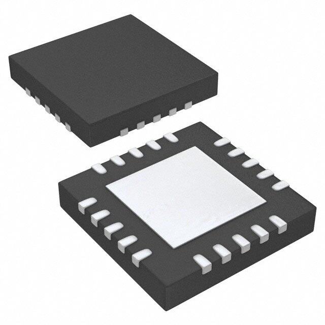
| 产品图片 |
|
| rohs | 符合RoHS无铅 / 符合限制有害物质指令(RoHS)规范要求 |
| 产品系列 | 接口 IC,I2C 接口集成电路,Intersil ISL33001IUZ- |
| 数据手册 | |
| 产品型号 | ISL33001IUZ |
| Tx/Rx类型 | I²C 逻辑 |
| 产品种类 | I2C 接口集成电路 |
| 供应商器件封装 | 8-MSOP |
| 包装 | 管件 |
| 商标 | Intersil |
| 安装类型 | 表面贴装 |
| 封装 | Tube |
| 封装/外壳 | 8-TSSOP,8-MSOP(0.118",3.00mm 宽) |
| 封装/箱体 | MSOP |
| 工作温度 | -40°C ~ 85°C |
| 工厂包装数量 | 50 |
| 应用 | I²C - 热插拔 |
| 延迟时间 | - |
| 数据速率(最大值) | - |
| 最大工作温度 | + 85 C |
| 最小工作温度 | - 40 C |
| 标准包装 | 50 |
| 电压-电源 | 2.3 V ~ 5.5 V |
| 电容-输入 | 10pF |
| 电流-电源 | 4mA |
| 类型 | 缓冲器, 加速计 |
| 系列 | ISL33001 |
| 输入 | 2 线式总线 |
| 输出 | 2 线式总线 |
| 通道数 | 2 |
| 配用 | /product-detail/zh/ISL33001MSOPEVAL1Z/ISL33001MSOPEVAL1Z-ND/2360890 |


- 商务部:美国ITC正式对集成电路等产品启动337调查
- 曝三星4nm工艺存在良率问题 高通将骁龙8 Gen1或转产台积电
- 太阳诱电将投资9.5亿元在常州建新厂生产MLCC 预计2023年完工
- 英特尔发布欧洲新工厂建设计划 深化IDM 2.0 战略
- 台积电先进制程称霸业界 有大客户加持明年业绩稳了
- 达到5530亿美元!SIA预计今年全球半导体销售额将创下新高
- 英特尔拟将自动驾驶子公司Mobileye上市 估值或超500亿美元
- 三星加码芯片和SET,合并消费电子和移动部门,撤换高东真等 CEO
- 三星电子宣布重大人事变动 还合并消费电子和移动部门
- 海关总署:前11个月进口集成电路产品价值2.52万亿元 增长14.8%


PDF Datasheet 数据手册内容提取
DATASHEET ISL33001, ISL33002, ISL33003 FN7560 I2C Bus Buffer with Rise Time Accelerators and Hot Swap Capability Rev 6.00 July 11, 2014 The ISL33001, ISL33002, ISL33003 are 2-Channel Bus Buffers Features that provide the buffering necessary to extend the bus capacitance beyond the 400pF maximum specified by the I2C • 2 Channel I2C compatible bi-directional buffer specification. In addition, the ISL33001, ISL33002, ISL33003 • +2.3VDC to +5.5VDC supply range feature rise time accelerator circuitry to reduce power • >400kHz operation consumption from passive bus pull-up resistors and improve data-rate performance. All devices also include hot swap circuitry • Bus capacitance buffering to prevent corruption of the data and clock lines when I2C devices • Rise time accelerators are plugged into a live backplane, and the ISL33002 and • Hot swapping capability ISL33003 add level translation for mixed supply voltage applications. The ISL33001, ISL33002, ISL33003 operate at • ±6kV Class 3 HBM ESD protection on all pins supply voltages from +2.3V to +5.5V at a temperature range of • ±12kV HBM ESD protection on SDA/SCL pins -40°Cto +85°C. • Enable pin (ISL33001 and ISL33003) Summary of Features • Logic level translation (ISL33002 and ISL33003) PART LEVEL ENABLE READY ACCELERATOR • READY logic pin (ISL33001) NUMBER TRANSLATION PIN PIN DISABLE • Accelerator disable pin (ISL33002) ISL33001 No Yes Yes No • Pb-free (RoHS Compliant) 8 Ld SOIC (ISL33001 only), ISL33002 Yes No No Yes 8LdTDFN (3mmx3mm) and 8Ld MSOP packages ISL33003 Yes Yes No No • Low quiescent current. . . . . . . . . . . . . . . . . . . . . . . 2.1mA typ • Low shutdown current. . . . . . . . . . . . . . . . . . . . . . . . 0.5µA typ Related Literature Applications •AN1543, “ISL33001MSOPEVAL1Z, ISL33002MSOPEVAL1Z, ISL33003MSOPEVAL1Z Evaluation Board User’s Manual” • I2C bus extender and capacitance buffering •AN1637, “Level Shifting Between 1.8V and 3.3V Using I2C • Server racks for telecom, datacom, and computer servers Buffers” • Desktop computers • Hot-swap board insertion and bus isolation 100kHz I2C BUS WITH 2.7kΩ PULL-UP RESISTOR AND 400pF BUS CAPACITANCE VCC1 +3.3V +5.0V VCC2 WITHOUT BUFFER µC BACK PLANE SSDCAL ISL33003 SSDCAL DEIV2ACICE 1V/DIV) EN E ( G WITH BUFFER A I2C LT DEVICE O B V GND TIME (2µs/DIV) FIGURE 1. TYPICAL OPERATING CIRCUIT FIGURE 2. BUS ACCELERATOR PERFORMANCE FN7560 Rev 6.00 Page 1 of 18 July 11, 2014
ISL33001, ISL33002, ISL33003 Ordering Information PART NUMBER PART TEMP. RANGE PACKAGE PKG. (Notes1, 2, 3) MARKING (°C) (Pb-free) DWG. # ISL33001IRTZ 3001 -40 to +85 8 Ld TDFN (0.65mm Pitch) L8.3x3A ISL33001IRT2Z 01R2 -40 to +85 8 Ld TDFN (0.5mm Pitch) L8.3x3H ISL33001IBZ 33001 IBZ -40 to +85 8 Ld SOIC M8.15 ISL33001IUZ 33001 -40 to +85 8 Ld MSOP M8.118 ISL33002IRTZ 3002 -40 to +85 8 Ld TDFN (0.65mm Pitch) L8.3x3A ISL33002IRT2Z 02R2 -40 to +85 8 Ld TDFN (0.5mm Pitch) L8.3x3H ISL33002IUZ 33002 -40 to +85 8 Ld MSOP M8.118 ISL33003IRTZ 3003 -40 to +85 8 Ld TDFN (0.65mm Pitch) L8.3x3A ISL33003IRT2Z 03R2 -40 to +85 8 Ld TDFN (0.5mm Pitch) L8.3x3H ISL33003IUZ 33003 -40 to +85 8 Ld MSOP M8.118 ISL33001MSOPEVAL1Z ISL33001 Evaluation Board ISL33002MSOPEVAL1Z ISL33002 Evaluation Board ISL33003MSOPEVAL1Z ISL33003 Evaluation Board NOTES: 1. Add “-T*” suffix for tape and reel. Please refer to TB347 for details on reel specifications. 2. These Intersil Pb-free plastic packaged products employ special Pb-free material sets, molding compounds/die attach materials, and 100% matte tin plate plus anneal (e3 termination finish, which is RoHS compliant and compatible with both SnPb and Pb-free soldering operations). Intersil Pb-free products are MSL classified at Pb-free peak reflow temperatures that meet or exceed the Pb-free requirements of IPC/JEDEC J STD-020. 3. For Moisture Sensitivity Level (MSL), please see device information page for ISL33001, ISL33002, ISL33003. For more information on MSL please see techbrief TB363. Pin Configurations ISL33001 ISL33001 (8 LD TDFN) (8 LD SOIC, MSOP) TOP VIEW TOP VIEW EN 1 8 VCC1 EN 1 8 VCC1 SCL_OUT 2 7 SDA_OUT SCL_OUT 2 7 SDA_OUT PAD SCL_IN 3 6 SDA_IN SCL_IN 3 6 SDA_IN GND 4 5 READY GND 4 5 READY ISL33002 ISL33002 (8 LD TDFN) (8 LD MSOP) TOP VIEW TOP VIEW VCC2 1 8 VCC1 VCC2 1 8 VCC1 SCL_OUT 2 7 SDA_OUT SCL_OUT 2 7 SDA_OUT PAD SCL_IN 3 6 SDA_IN SCL_IN 3 6 SDA_IN GND 4 5 ACC GND 4 5 ACC FN7560 Rev 6.00 Page 2 of 18 July 11, 2014
ISL33001, ISL33002, ISL33003 Pin Configurations (Continued) ISL33003 ISL33003 (8 LD TDFN) (8 LD MSOP) TOP VIEW TOP VIEW VCC2 1 8 VCC1 VCC2 1 8 VCC1 SCL_OUT 2 7 SDA_OUT SCL_OUT 2 7 SDA_OUT PAD SCL_IN 3 6 SDA_IN SCL_IN 3 6 SDA_IN GND 4 5 EN GND 4 5 EN Pin Descriptions PIN PIN NAME NUMBER FUNCTION NOTES VCC1 8 VCC1 power supply, +2.3V to +5.5V. Decouple VCC1 to ground with a high frequency 0.01µF to 0.1µF capacitor. VCC2 1 VCC2 power supply, +2.3V to +5.5V. Decouple VCC2 to ground with a high frequency ISL33002 (8 LD TDFN, 8 LD MSOP) 0.01µF to 0.1µF capacitor. In level shifting applications, SDA_OUT and SCL_OUT logic ISL33003 (8 LD TDFN, 8 LD MSOP) thresholds are referenced to VCC2 supply levels. Connect pull-up resistors on these pins to VCC2. GND 4 Device Ground Pin EN 1 Buffer Enable Pin. Logic “0” disables the device. Logic “1” enables the device. Logic ISL33001 (8 LD TDFN, 8 LD SOIC, MSOP) threshold referenced to VCC1. 5 ISL33003 (8 LD TDFN, 8 LD MSOP) READY 5 Buffer active ‘Ready’ open drain logic output. When buffer is active, READY is high ISL33001 only impedance. When buffer is inactive, READY is low impedance to ground. Connect to 10kΩ pull-up resistor to VCC1. ACC 5 Rise Time Accelerator Enable Pin. Logic “0” disables the accelerator. Logic “1” ISL33002 only enables the accelerator. Logic threshold referenced to VCC1. SDA_IN 6 Data I/O Pins SDA_OUT 7 SCL_IN 3 Clock I/O Pins SCL_OUT 2 PAD Thermal pad should be connected to ground or floated. Thermal Pad; TDFN only FN7560 Rev 6.00 Page 3 of 18 July 11, 2014
ISL33001, ISL33002, ISL33003 Absolute Maximum Ratings Thermal Information (Allvoltagesreferencedto GND) VCC1, VCC2. . . . . . . . . . . . . . . . . . . . . . . . . . . . . . . . . . . . . . . . . . -0.3V to +7V Thermal Resistance JA (°C/W) JC (°C/W) SDA_IN, SCL_IN, SDA_OUT, SCL_OUT, READY. . . . . . . . . . . . . -0.3V to +7V 8 Ld TDFN Package (Notes5, 6). . . . . . . . . . 47 4 EN, ACC . . . . . . . . . . . . . . . . . . . . . . . . . . . . . . . . . . . -0.3V to +(VCC1 + 0.3)V (0.50mm Pitch) Maximum Sink Current (SDA and SCL Pins). . . . . . . . . . . . . . . . . . . . 20mA 8 Ld TDFN Package (Notes5, 6). . . . . . . . . . 48 6 Maximum Sink Current (READY pin) . . . . . . . . . . . . . . . . . . . . . . . . . . . 7mA (0.65mm Pitch) Latch-Up Tested per JESD78, Level 2, Class A . . . . . . . . . . . . . . . . . . 85°C 8 Ld MSOP Package (Notes4, 7) . . . . . . . . . 151 50 ESD Ratings. . . . . . . . . . . . . . . . . . . . . . See “ESD PROTECTION” on page5 8 Ld SOIC Package (Notes4, 7) . . . . . . . . . . 120 56 Maximum Storage Temperature Range . . . . . . . . . . . . . -65°C to +150°C Operating Conditions Maximum Junction Temperature . . . . . . . . . . . . . . . . . . . . . . . . . . . +150°C Pb-Free Reflow Profile . . . . . . . . . . . . . . . . . . . . . . . . . . . . . . . . . . see TB493 Temperature Range, TA. . . . . . . . . . . . . . . . . . . . . . . . . . . . -40°C to +85°C VCC1 and VCC2 Supply Voltage Range. . . . . . . . . . . . . . . . . +2.3V to +5.5V CAUTION: Do not operate at or near the maximum ratings listed for extended periods of time. Exposure to such conditions may adversely impact product reliability and result in failures not covered by warranty. NOTES: 4. JA is measured with the component mounted on a high effective thermal conductivity test board in free air. See Tech Brief TB379 for details. 5. JA is measured in free air with the component mounted on a high effective thermal conductivity test board with “direct attach” features. See Tech Brief TB379. 6. For JC, the “case temp” location is the center of the exposed metal pad on the package underside. 7. For JC, the “case temp” location is taken at the package top center. Electrical Specifications VEN = VCC1, VCC1 = +2.3V to +5.5V, VCC2 = +2.3V to +5.5V, unless otherwise noted (Note8). Boldface limits apply over the operating temperature range, -40°C to +85°C. TEMP MIN MAX PARAMETER SYMBOL CONDITIONS (°C) (Note9) TYP (Note9) UNITS POWER SUPPLIES VCC1 Supply Range VCC1 Full 2.3 - 5.5 V VCC2 Supply Range VCC2 ISL33002 and ISL33003 Full 2.3 - 5.5 V Supply Current from VCC1 ICC1 VCC1 = 5.5V; ISL33001 only (Note11) Full - 2.1 4.0 mA VCC1 = VCC2 = 5.5V; ISL33002 and ISL33003 Full - 2.0 3.0 mA (Note11) Supply Current from VCC2 ICC2 VCC2 = VCC1 = 5.5V; ISL33002 and ISL33003 Full - 0.22 0.6 mA (Note11) VCC1 Shut-down Supply ISHDN1 VCC1 = 5.5V, VEN = GND; ISL33001 only Full - 0.5 - µA Current VCC1 = VCC2 = 5.5V, VEN = GND; ISL33003only Full - 0.05 - µA (Note13) VCC2 Shut-down Supply ISHDN2 VCC1 = VCC2 = 5.5V, VEN = GND, ISL33003only Full - 0.06 - µA Current (Note13) START-UP CIRCUITRY Precharge Circuitry VPRE SDA and SCL pins floating Full 0.8 1 1.2 V Voltage Enable High Threshold VEN_H +25 - 0.5*VCC 0.7*VCC V Voltage Enable Low Threshold VEN_L +25 0.3*VCC 0.5*VCC - V Voltage Enable Pin Input Current IEN Enable from 0V to VCC1; ISL33001 and Full -1 0.1 1 µA ISL33003 Enable Delay, On-Off tEN-HL ISL33001 and ISL33003 (Note10) +25 - 10 - ns Enable Delay, Off-On tEN-LH ISL33001 and ISL33003 (Figure3) +25 - 86 - µs Bus Idle Time tIDLE (Figure4, Note12) Full 50 83 150 µs Ready Pin OFF State IOFF ISL33001 only +25 -1 0.1 1 µA Leakage Current Ready Delay, On-Off tREADY-HL ISL33001 only (Note10) +25 - 10 - ns FN7560 Rev 6.00 Page 4 of 18 July 11, 2014
ISL33001, ISL33002, ISL33003 Electrical Specifications VEN = VCC1, VCC1 = +2.3V to +5.5V, VCC2 = +2.3V to +5.5V, unless otherwise noted (Note8). Boldface limits apply over the operating temperature range, -40°C to +85°C. (Continued) TEMP MIN MAX PARAMETER SYMBOL CONDITIONS (°C) (Note9) TYP (Note9) UNITS Ready Delay, Off-On tREADY-LH ISL33001 only (Note10) +25 - 10 - ns Ready Output Low Voltage VOL_READY VCC1 = +2.5V, IPULLUP = 3mA; ISL33001 only Full - - 0.4 V RISE-TIME ACCELERATORS Transient Accelerator ITRAN_ACC VCC1 = 2.7V, VCC2 = 2.7V ; (ACC=0.7*VCC1 for +25 - 5 - mA Current ISL33002 only) (Figure8) Accelerator Pin Enable VACC_EN ISL33002 only +25 - 0.5*VCC1 0.7*VCC1 V Threshold Accelerator Pin Disable VACC_DIS ISL33002 only +25 0.3*VCC1 0.5*VCC1 - V Threshold Accelerator Pin Input IACC ISL33002 only +25 -1 0.1 1 µA Current Accelerator Delay, On-Off tPDOFF ISL33002 only (Note10) +25 - 10 - ns ESD PROTECTION SDA, SCL I/O Pins Human Body Model, SDA and SCL pins to ground +25 - ±12 - kV only (JESD22-A114) All Pins Machine Model (JESD22-A115) +25 - ±400 - V Class 3 HBM ESD (JESD22-A114) +25 ±6 - kV INPUT-OUTPUT CONNECTIONS Input Low Threshold VIL VCC1 = VCC2, 10kto VCC1 on SDA and SCL pins +25 - - 0.3*VCC1 V Input-Output Offset VOS VCC1 = 3.3V, 10kto VCC1 on SDA and SCL pins, Full 0 50 150 mV Voltage VINPUT = 0.2V; VCC2 = 3.3V, ISL33002 and ISL33003 (Figure5) Output Low Voltage VOL VCC1 = 2.7V, VINPUT = 0V, ISINK =3mA on Full - - 0.4 V SDA/SCL pins; VCC2 = 2.7V, ISL33002 and ISL33003 (Figure6) Buffer SDA and SCL Pins CIN (Figure25) +25 - 10 - pF Input Capacitance Input Leakage Current ILEAK SDA and SCL pins = VCC1 = 5.5V; Full -5 0.1 5 µA VCC2 = 5.5V, ISL33002 and ISL33003 TIMING CHARACTERISTICS SCL/SDA Propagation tPHL CLOAD = 100pF, 2.7kto VCC1 on SDA and SCL +25 0 27 100 ns Delay High-to-Low pins, VCC1 = 3.3V; VCC2= 3.3V, ISL33002 and ISL33003 (Figure7) SCL/SDA Propagation tPLH CLOAD = 100pF, 2.7kto VCC1 on SDA and SCL +25 0 2 26 ns Delay Low-to-High pins, VCC1 = 3.3V; VCC2= 3.3V, ISL33002 and ISL33003 (Figure7) NOTES: 8. The algebraic convention, whereby the most negative value is a minimum and the most positive a maximum, is used in this data sheet. 9. Parameters with MIN and/or MAX limits are 100% tested at +25°C, unless otherwise specified. Temperature limits established by characterization and are not production tested. 10. Typical value determined by design simulations. Parameter not tested. 11. Buffer is in the connected state. 12. ISL33002 and ISL33003 limits established by characterization. Not production tested. 13. If the VCC1 and VCC2 voltages diverge, then the shut down ICC increases on the higher voltage supply. FN7560 Rev 6.00 Page 5 of 18 July 11, 2014
ISL33001, ISL33002, ISL33003 Test Circuits and Waveforms - SDA_OUT and SCL pins connected to VCC - VSDA_IN = VSDA_OUT = VSCL_OUT = VEN = VCC - Enable Delay Time Measured on ISL33001 only - EN Logic Input must be high for t > Enable Delay (tEN_LH) - ISL33003 performance inferred from ISL33001 prior to SCL_IN transition - If tDELAY1 < tEN-LH then tDELAY2 = tEN-LH + tIDLE + tREADY-LH - Bus Idle Time Measured on ISL33001 only - If tDELAY1 > tEN-LH then tDELAY2 = tEN-LH + tREADY-LH - ISL33002 and ISL33003 performance inferred from ISL33001 VEN VCC 0.5*VCC VCC 0V VSCL_IN 0.5VCC VSDA_IN VREADY 0V VCC 0.5*VCC 0.5*VCC VCC 0.5VCC 0V VREADY 0V tDELAY1 tREADY-LH tDELAY2 tIDLE FIGURE 3. ENABLE DELAY TIME FIGURE 4. BUS IDLE TIME +3.3V 0.2V 10kΩ 10kΩ 10kΩ SCL_IN OR VCC1 SDA_IN SCL_OUT SDA_OUT 10kΩ SCL_IN SDA_IN GND SCL_OUT OR VO VIN VIN SDA_OUT 0.2V 0.2V VOS = VO - 0.2V FIGURE 5A. TEST CIRCUIT FIGURE 5B. MEASUREMENT POINTS FIGURE 5. INPUT TO OUTPUT OFFSET VOLTAGE +2.7V 900Ω 900Ω 900Ω VCC1 VCC1 SCL_OUT SDA_OUT 900Ω VOL SCL_IN SDA_IN SCL_OUT GND VCC1 0V 0V VOL SDA_OUT FIGURE 6A. TEST CIRCUIT FIGURE 6B. MEASUREMENT POINTS FIGURE 6. OUTPUT LOW VOLTAGE FN7560 Rev 6.00 Page 6 of 18 July 11, 2014
ISL33001, ISL33002, ISL33003 Test Circuits and Waveforms (Continued) +3.3V SCL_IN OR SDA_IN 2.7kΩ 2.7kΩ 2.7kΩ VCC1 SCL_OUT SDA_OUT 2.7kΩ SCL_IN SDA_IN SCL_OUT OR SDA_OUT GND VIN 100pF VIN *tPLH *tPHL 100pF 100pF 100pF *Propagation delay measured between 50% of VCC1 FIGURE 7A. TEST CIRCUIT FIGURE 7B. MEASUREMENT POINTS FIGURE 7. PROPAGATION DELAY ITRAN_ACC = CV/t poVr/tito ins ofof rt hoen wlya tvheef oarcmcelerator VCC1 *VX VCC1 *VX 2.7kΩ 2.7kΩ 2.7kΩ 10kΩ 10kΩ 10kΩ 10kΩ 100kΩ SCL_OUT VCC1 SDA_OUT SCL_OUT VCC1 SDA_OUT SCL_IN SDA_IN SCL_IN SDA_IN GND GND 2nF *VX < VCC1 (See Figure22) FIGURE 8. ACCELERATOR CURRENT TEST CIRCUIT FIGURE 9. ACCELERATOR PULSE WIDTH TEST CIRCUIT FN7560 Rev 6.00 Page 7 of 18 July 11, 2014
ISL33001, ISL33002, ISL33003 SDA_IN U1 SDA_OUT M2 M1 U2 READY RISE TIME ISL33001 ONLY ACCELERATOR M5 LOGIC CONTROL START-UP CIRCUITRY VCC1 VCC2 ISL33002 AND ISL33003 EN ACC ISL33001 AND ISL33003 PRECHARGE ISL33002 ONLY CIRCUIT SCL_IN U3 SCL_OUT M4 M3 U4 FIGURE 10. CIRCUIT BLOCK DIAGRAM Application Information Start-Up Sequencing and Hot Swap Circuitry The ISL33001, ISL33002, ISL33003 buffers contain The ISL33001, ISL33002, ISL33003 ICs are 2-Wire Bidirectional undervoltage lock out (UVLO) circuitry that prevents operation of Bus Buffers designed to drive heavy capacitive loads in the buffer until the IC receives the proper supply voltage. For open-drain/open-collector systems. The ISL33001, ISL33002, ISL33003 incorporate rise time accelerator circuitry that VCC1 and VCC2, this voltage is approximately 1.8V on the rising edge of the supply voltage. Externally driven signals at the improves the rise time for systems that use a passive pull-up SDA/SCL pins are ignored until the device supply voltage is resistor for logic HIGH. These devices also feature hot swapping above 1.8V. This prevents communication errors on the bus until circuitry for applications that require hot insertion of boards into the device is properly powered up. The UVLO circuitry is also a host system (i.e., servers racks and I/O card modules). The triggered on the falling edge when the supply voltage drops ISL33001 features a logic output flag (READY) that signals the below 1.7V. status of the buffer and an EN pin to enable or disable the buffer. The ISL33002 features two separate supply pins for voltage level Once the IC comes out of the UVLO state, the buffer remains shifting on the I/O pins and a logic input to disable the rise time disconnected until it detects a valid connection state. A valid accelerator circuitry. The ISL33003 features an EN pin and the connection state is either a BUS IDLE condition (see Figure4) or a level shifting functionality. STOP BIT condition (a rising edge on SDA_IN when SCL_IN is high) 2 along with the SCL_OUT and SDA_OUT pins being logic high. I C and SMBUS Compatibility Note: For the ISL33001 and ISL33003 with EN pins, after coming The ISL33001, ISL33002, ISL33003 ICs are I2C and SMBUS out of UVLO, there will be an additional delay from the enable compatible devices, designed to work in open-drain/open-collector circuitry if the EN pin voltage is not rising at the same time as the bus environments. The ICs support both clock stretching and bus supply pins (see Figure3) before a valid connection state can be arbitration on the SDA and SCL pins. They are designed to operate established. from DC to more than 400kHz, supporting Fast Mode data rates of the I2C specification.In addition, the buffer rise time accelerators Coming out of UVLO but prior to a valid connection state, the SDA are designed to increase the capacitive drive capability of the bus. and SCL pins are pre-charged to 1V to allow hot insertion. With careful choosing of components, driving a bus with the I2C Because the bus at any time can be between 0V and VCC, specified maximum bus capacitance of 400pF at 400kHz data rate pre-charging the I/O pins to 1V reduces the maximum is possible. differential voltage from the buffer I/O pin and the active bus. FN7560 Rev 6.00 Page 8 of 18 July 11, 2014
ISL33001, ISL33002, ISL33003 The pre-charge circuitry reduces system disturbance when the IC performance. The rise time accelerators are only active on the is hot plugged into a live back plane that may have the bus low-to-high transitions and provide an active constant current communicating with other devices. source to slew the voltage on the pin quickly (Figure21). Note: For The ISL33001 and ISL33003 with EN pins, the The rise time accelerators are triggered immediately after the pre-charge circuitry is active only after coming out of UVLO and buffer release threshold (approximately 30% of VCC) on both having the device enabled. sides of the buffer is crossed. Once triggered, the accelerators are active for a defined pulse width (Figure22) with the current Connection Circuitry source turning off as it approaches the supply voltage. Once a valid connection condition is met, the buffer is active and Enable Pin (ISL33001 and ISL33003) the input stage of the SDA/SCL pins is controlled by external drivers. The output of the buffer will follow the input of the buffer. When driven high, the enable pin puts the buffer into its normal The directionality of the IN/OUT pins are not exclusive operating state. After power-up, EN high will activate the bus (bi-directional operation) and functionally behave identical to pre-charge circuitry and wait for a valid connection state to each other. Being a two channel buffer, the SDA and SCL pins enable the buffer and the accelerator circuitry. also behave identically. In addition, the SDA and SCL portions of Driving the EN pin low disables the accelerators, disables the the buffer are independent from each other. The SDA pins can be buffer so that signals on one side of the buffer will be isolated driven in one direction while the SCL pins can be driven opposite. from the other side, disables the pre-charge circuit and places Refer to Figure10 for the operation of the bi-directional buffer. the device in a low power shutdown state. When the input stage of the buffer on one side is driven low by an READY Logic Pin (ISL33001 Only) external device, the output of the buffer drives an open-drain transistor to pull the ‘output’ pin low. The ‘output’ pin will The READY pin is a digital output flag for signaling the status of continue to be held low by the transistor until the external driver the buffer. The pin is the drain of an Open-Drain NMOS. Connect on the ‘input’ releases the bus. a resistor from the READY pin to VCC1 to provide the high pull-up. To prevent the buffer from entering a latched condition where The recommended value is 10kΩ. both internal transistors are actively pulling the I/O pins low, the When the buffer is disabled by having the EN pin low or if the buffer is designed to be active in only one direction. The buffer start-up sequencing is not complete, the READY pin will be pulled logic circuitry senses, which input stage is being externally driven low by the NMOS. When the buffer has the EN pin high and a low and sets that buffer to be the active one. For example, valid connection state is made at the SDA/SCL pins, the READY referring to Figure10, if SDA_OUT is externally driven low, buffer pin will be pulled high by the pull-up resistor. The READY pin is U2 will be active and buffer U1 is inactive. M1 is turned on to capable of sinking 3mA when pulled low while maintaining a drive SDA_IN low, effectively buffering the signal from SDA_OUT voltage of less than 0.4V. to SDA_IN. The low signal at the input of U1 will not turn M2 on because U1 remains inactive, preventing a latch condition. ACC Accelerator Pin (ISL33002 Only) Buffer Output Low and Offset Voltage The ACC logic pin controls the rise time accelerator circuitry of the buffer. When ACC is driven high, the accelerators are enabled By design, when a logic input low voltage is forced on the input of and will be triggered when crossing the buffer release threshold. the buffer, the output of the buffer will have an input to output When ACC is driven low, the accelerators are disabled. offset voltage. The output voltage of the buffer is determined by Equation1: For lightly loaded buses, having the accelerators active may cause ringing or noise on the rising edge transition. Disabling the V = V +V +V /R r (EQ. 1) OUT IN OS CC PULL-UP ON accelerators will have the buffers continue to perform level Where VOS is the buffer internal offset voltage, RPull-Up is the schaipfaticnigta wnicteh bthueff VeCriCn1g .and VCC2 supplies and provide pull-up resistance on the SDA/SCL pin to VCC and rON is the ON-resistance of the buffer’s internal NMOS pull-down device. Propagation Delays The last term of the equation is the additional voltage drop developed by sink current and the internal resistance of the On a low-to-high transition, the rising edge signal is determined transistor. The VOS of the buffer can be determined by by the bus pull-up resistor, load capacitance, and the accelerator Figures19, 20 and is typically 40mV. Reducing the pull-up current from the ISL33001, ISL33002, ISL33003 buffer. Prior to resistor values increases the sink current and increases the the accelerators becoming active, the buffer is connected and output voltage of the buffer for a given input low voltage the output voltage will track the input of the buffer. When the (Figures17, through 20). accelerators activate the buffer connection is released and the signal on each side of the buffer rises independently. The Rise Time Accelerators accelerator current on both sides of the buffer will be equal. If the pull-up resistance on both sides of the buffer are also equal, then The ISL33001, ISL33002, ISL33003 buffer rise time differences in the rise time will be proportional to the difference accelerators on the SDA/SCL pins improve the transient in capacitive loading on the two sides. performance of the system. Heavy load capacitance or weak pull-up resistors on an Open-Drain bus cause the rise time to be excessively long, which leads to data errors or reduced data rate FN7560 Rev 6.00 Page 9 of 18 July 11, 2014
ISL33001, ISL33002, ISL33003 Because the signals on each side of the buffer rise independently, the propagation delay can be positive or negative. If the input side rises slowly relative to the output (i.e., heavy capacitive loading on the input and light load on the output) then the propagation delay tPLH is negative. If the output side rises slowly relative to the input, tPLH is positive. For high-to-low transitions, there is a finite propagation delay through the buffer from the time an external low on the input drives the NMOS output low. This propagation delay will always be positive because the buffer connect threshold on the falling edge is below the measurement points of the delay. In addition to the propagation delay of the buffer, there will be additional delay from the different capacitive loading of the buffer. Figures23 and 24 show how the propagation delay from high-to- low, tPHL, is affected by VCC and capacitive loading. The buffer’s propagation delay times for rising and falling edge signals must be taken into consideration for the timing requirements of the system. SETUP and HOLD times may need to be adjusted to take into account excessively long propagation delay times caused by heavy bus capacitances. Pull-Up Resistor Selection While the ISL33001, ISL33002, ISL33003 2-Channel buffers are designed to improve the rise time of the bus in passive pull-up systems, proper selection of the pull-up resistor is critical for system operation when a buffer is used. For a bus that is operating normally without active rise time circuitry, using the ISL33001, ISL33002, ISL33003 buffer allows larger pull-up resistor values to reduce sink currents when the bus is driving low. However, choose a pull-up resistor value of no larger than 20kΩ regardless of the bus capacitance seen on the SDA/SCL lines. The Bus Idle or Stop Bit condition requires valid logic high voltages to give a valid connection state. Pull-up resistor values 20kΩ or smaller are recommended to overcome the typical 150kΩ impedance of the pre-charge circuitry, delivering valid high levels. FN7560 Rev 6.00 Page 10 of 18 July 11, 2014
ISL33001, ISL33002, ISL33003 Typical Performance Curves CIN = COUT = 10pF, VCC1 = VCC2 = VCC, TA = +25°C; Unless Otherwise Specified. 2.4 600 2.3 T = -40°C 550 2.2 500 2.1 T = +25°C 450 T = +25°C 2.0 T = +85°C A) 1.9 A) 400 T = +85°C m n (C1 1.8 (C1 350 IC 1.7 IC 300 1.6 250 1.5 200 1.4 150 1.3 1.2 100 2.0 2.5 3.0 3.5 4.0 4.5 5.0 5.5 6.0 2.0 2.5 3.0 3.5 4.0 4.5 5.0 5.5 6.0 VCC1 (V) VCC1 (V) FIGURE 11. ICC1 ENABLED CURRENT vs VCC1 (ISL33001) FIGURE 12. ICC1 DISABLED CURRENT vs VCC1 (ISL33001) 2.4 60 2.3 VCC2 = 5.5V VCC2 = 5.5V 2.2 50 2.1 T = +85°C T = -40°C 2.0 40 T = +25°C A) 1.9 A) (mC1 1.8 (nC1 30 T = +85°C T = +25°C C 1.7 C I I 1.6 20 1.5 1.4 10 1.3 1.2 0 2.0 2.5 3.0 3.5 4.0 4.5 5.0 5.5 6.0 2.0 2.5 3.0 3.5 4.0 4.5 5.0 5.5 6.0 VVCCCC11 ((VV)) VCC1 (V) FIGURE 13. ICC1 ENABLED CURRENT vs VCC1 (ISL33002 AND FIGURE 14. ICC1 DISABLED CURRENT vs VCC1 (ISL33003) ISL33003) 0.24 60 VCC1 = 5.5V T = +25°C VCC1 = 5.5V 0.22 50 T = -40°C 0.20 T = +85°C 40 A) 0.18 A) m n I (CC2 0.16 I (CC2 30 T = +85°C T = +25°C 20 0.14 10 0.12 0.10 0 2.0 2.5 3.0 3.5 4.0 4.5 5.0 5.5 6.0 2.0 2.5 3.0 3.5 4.0 4.5 5.0 5.5 6.0 VCC2 (V) VCC2 (V) FIGURE 15. ICC2 ENABLED CURRENT vs VCC2 (ISL33002 AND FIGURE 16. ICC2 DISABLED CURRENT vs VCC2 (ISL33003) ISL33003) FN7560 Rev 6.00 Page 11 of 18 July 11, 2014
ISL33001, ISL33002, ISL33003 Typical Performance Curves (Continued) CIN = COUT = 10pF, VCC1 = VCC2 = VCC, TA = +25°C; Unless Otherwise 120 120 T = -40°C VCC = 2.3V 100 100 T = +25°C T = +85°C 80 80 mV) mV) V (OL 60 VCC = 2.7V V (OL 60 40 40 VCC = 4.5V 20 20 VCC = 3.3V VIN = 0V VIN = 0V 0 0 0 1 2 3 4 5 6 7 8 9 10 11 0 1 2 3 4 5 6 7 8 9 10 11 IOL (mA) IOL (mA) FIGURE 17. SDA/SCL OUTPUT LOW VOLTAGE vs SINK CURRENT vs VCC FIGURE 18. SDA/SCL OUTPUT LOW VOLTAGE vs SINK CURRENT vs TEMPERATURE 100 100 T = -40°C 90 VCC = 5.5V 90 T = +25°C 80 80 T = +85°C 70 70 V) 60 V) 60 m m (S 50 VCC = 3.3V (S 50 VO 40 VCC = 2.3V VO 40 30 30 20 20 VCC = 3.3V 10 VIN = 0.2V 10 VIN = 0.2V 0 0 0 1 2 3 4 5 6 7 8 9 10 11 0 1 2 3 4 5 6 7 8 9 10 11 IOL (mA) IOL (mA) FIGURE 19. INPUT TO OUTPUT OFFSET VOLTAGE vs SINK CURRENT FIGURE 20. INPUT TO OUTPUT OFFSET VOLTAGE vs SINK CURRENT vs VCC vs TEMPERATURE 12 800 mA) 11 T = -40°C H (ns) 700 See Figure9 T ( 10 DT T = +25°C REN 9 E WI 600 T = +85°C T = -40°C R S U 8 L R C T = +85°C PU 500 O 7 R T O A T R 6 A 400 E R L E CE 5 T = +25°C EL C C 300 A 4 C A 3 200 2.0 2.5 3.0 3.5 4.0 4.5 5.0 5.5 6.0 2.0 2.5 3.0 3.5 4.0 4.5 5.0 5.5 6.0 VCC (V) VCC (V) FIGURE 21. ACCELERATOR PULL-UP CURRENT vs VCC FIGURE 22. ACCELERATOR PULSE WIDTH vs VCC FN7560 Rev 6.00 Page 12 of 18 July 11, 2014
ISL33001, ISL33002, ISL33003 Typical Performance Curves (Continued) CIN = COUT = 10pF, VCC1 = VCC2 = VCC, TA = +25°C; Unless Otherwise 50 50 RPULL-UP = 2.7kΩ T = +85°C CIN = 10pF T = +85°C COUT = 100pF 40 40 s) s) n n AY ( T = +25°C AY ( EL 30 EL 30 D D N N O O TI TI T = +25°C GA 20 T = -40°C GA 20 A A P P O O T = -40°C R R P P VCC = 3.3V 10 10 RPULL-UP = 10kΩ CIN = 50pF 0 0 2.0 2.5 3.0 3.5 4.0 4.5 5.0 5.5 6.0 0 100 200 300 400 500 600 700 800 900 VCC (V) COUT (pF) FIGURE 23. PROPAGATION DELAY H-L vs VCC FIGURE 24. PROPAGATION DELAY H-L vs COUT Die Characteristics 12 SUBSTRATE AND TDFN THERMAL PAD POTENTIAL (POWERED UP): 11 VCC = 2.3V VCC = 3.3V VCC = 5.5V GND F) 10 p PROCESS: E ( C 0.25µm CMOS N A 9 T CI A P A 8 C 7 6 -30 -10 10 30 50 70 90 TEMPERATURE (°C) FIGURE 25. SDA/SCL PIN CAPACITANCE vs TEMPERATURE vs VCC © Copyright Intersil Americas LLC 2010-2014. All Rights Reserved. All trademarks and registered trademarks are the property of their respective owners. For additional products, see www.intersil.com/en/products.html Intersil products are manufactured, assembled and tested utilizing ISO9001 quality systems as noted in the quality certifications found at www.intersil.com/en/support/qualandreliability.html Intersil products are sold by description only. Intersil may modify the circuit design and/or specifications of products at any time without notice, provided that such modification does not, in Intersil's sole judgment, affect the form, fit or function of the product. Accordingly, the reader is cautioned to verify that datasheets are current before placing orders. Information furnished by Intersil is believed to be accurate and reliable. However, no responsibility is assumed by Intersil or its subsidiaries for its use; nor for any infringements of patents or other rights of third parties which may result from its use. No license is granted by implication or otherwise under any patent or patent rights of Intersil or its subsidiaries. For information regarding Intersil Corporation and its products, see www.intersil.com FN7560 Rev 6.00 Page 13 of 18 July 11, 2014
ISL33001, ISL33002, ISL33003 Revision History The revision history provided is for informational purposes only and is believed to be accurate, but not warranted. Please go to web to make sure you have the latest revision. DATE REVISION CHANGE July 11, 2014 FN7560.6 In “Features” on page1, changed “Low quiescent Current” from “2.2mA” to “2.1mA”. On page4, added “Pb-Free Reflow Profile” entry to “Thermal Info” section. In “Electrical Spec” table on page4, changed “VCC” to “VCC1” in the “Supply Current from VCC2” row. In “Electrical Spec” table on page5, for parameter “Input Low Threshold”, moved the “TYP” column entry to the “MAX” column. On page6, Figure4, clarified the associated notes. On page7, Figure8, changed “IACC” to ITRAN_ACC”, and noted that the V/t is for the accelerator portion of the waveform. December 19, 2013 FN7560.5 Added Note 13 at the end of the "Elec Spec" table on page5 as follows: “13. If the Vcc1 and Vcc2 voltages diverge, then the shut-down Icc increases on the higher voltage supply." Added reference "(Note 13)" after "ISL33003 only" in rows for Vcc1 and Vcc2 "Shut-down Supply current" parameters (last 2 rows of "Power Supplies" section) on page4. October 12, 2012 FN7560.4 Changed “SDA_IN, SCL_IN...0.3V to +(VCC1 + 0.3)V, SDA_OUT, SCL_OUT...0.3V to +(VCC2 + 0.3)V, ENABLE, READY, ACC...0.3V to +(VCC1 + 0.3)V” to “SDA_IN, SCL_IN, SDA_OUT, SCL_OUT, READY...0.3V to +7V; ENABLE, ACC...0.3V to +(VCC1 + 0.3)V”, in the Absolute Maximum Ratings section at the top of page4. Removed “Pb-free Reflow Profile” and link from “Thermal Information” section at the top of page4. Added “open drain” and “Connect to 10kΩ pull-up resistor to VCC1.”, in Pin Descriptions in the READY section on page3. October 11, 2011 FN7560.3 Converted to new datasheet template. Changed Title of datasheet from: “2-Wire Bus Buffer With Rise Time Accelerators and Hot Swap Capability” to: I2C Bus Buffer with Rise Time Accelerators and Hot Swap Capability Pg 1, added to Related Literature: AN1637, “Level Shifting Between 1.8V and 3.3V Using I2C Buffers” Replaced POD M8.118 Rev 3 with Rev 4 due to the following changes: Corrected lead width dimension in side view 1 from "0.25 - 0.036" to "0.25 - 0.36" Replaced POD M8.15 Rev 1 with Rev 3 due to the following changes: Changed in Typical Recommended Land Pattern the following: 2.41(0.095) to 2.20(0.087) 0.76 (0.030) to 0.60(0.023) 0.200 to 5.20(0.205) Figure 3 (was Fig1) - Added: - If tDELAY1 < tEN-LH then tDELAY2 = tEN-LH + tIDLE + tREADY-LH - If tDELAY1 > tEN-LH then tDELAY2 = tEN-LH + tREADY-LH and replaced graph September 13, 2010 FN7560.2 Added SOIC package information to datasheet for ISL33001. April 30, 2010 FN7560.1 Changed typical value of “Supply Current from VCC1” on page4 for ISL33001 only from 2.2mA to 2.1mA. Changed typical value of “Input-Output Offset Voltage” on page5 from 100mV to 50mV. March 18, 2010 FN7560.0 Initial Release. About Intersil Intersil Corporation is a leading provider of innovative power management and precision analog solutions. The company's products address some of the largest markets within the industrial and infrastructure, mobile computing and high-end consumer markets. For the most updated datasheet, application notes, related documentation and related parts, please see the respective product information page found at www.intersil.com. You may report errors or suggestions for improving this datasheet by visiting www.intersil.com/ask. Reliability reports are also available from our website at www.intersil.com/support FN7560 Rev 6.00 Page 14 of 18 July 11, 2014
ISL33001, ISL33002, ISL33003 Package Outline Drawing L8.3x3H 8 LEAD THIN DUAL FLAT NO-LEAD PLASTIC PACKAGE (TDFN) Rev 0, 2/08 2.38 1.50 REF 3.00 A PIN #1 INDEX AREA 6 X 0.50 6 6 PIN 1 INDEX AREA B 1 4 8 X 0.40 2.20 3.00 1.64 (4X) 0.15 8 5 TOP VIEW 0.10M C AB 8 X 0.25 BOTTOM VIEW ( 2.38 ) SEE DETAIL "X" 0 .80 MAX 0.10 C C BASE PLANE SEATING PLANE 0.08 C 2 . 80 ( 2 .20 ) SIDE VIEW ( 1.64 ) 0.2 REF C 8X 0.60 0 . 00 MIN. 0 . 05 MAX. ( 8X 0.25 ) DETAIL “X” ( 6X 0 . 5 ) NOTES: TYPICAL RECOMMENDED LAND PATTERN 1. Dimensions are in millimeters. Dimensions in ( ) for Reference Only. 2. Dimensioning and tolerancing conform to AMSE Y14.5m-1994. 3. Unless otherwise specified, tolerance : Decimal ± 0.05 4. Lead width dimension applies to the metallized terminal and is measured between 0.15mm and 0.30mm from the terminal tip. 5. Tiebar shown (if present) is a non-functional feature. 6. The configuration of the pin #1 identifier is optional, but must be located within the zone indicated. The pin #1 identifier may be either a mold or mark feature. FN7560 Rev 6.00 Page 15 of 18 July 11, 2014
ISL33001, ISL33002, ISL33003 Package Outline Drawing L8.3x3A 8 LEAD THIN DUAL FLAT NO-LEAD PLASTIC PACKAGE Rev 4, 2/10 ( 2.30) 3.00 A ( 1.95) B ( 8X 0.50) 6 00 (1.50) 3. PIN 1 ( 2.90 ) INDEX AREA (4X) 0.15 PIN 1 TOP VIEW (6x 0.65) ( 8 X 0.30) TYPICAL RECOMMENDED LAND PATTERN SEE DETAIL "X" 2X 1.950 0.10C C 6X 0.65 0.75 ±0.05 PIN #1 1 0.08C INDEX AREA SIDE VIEW 6 1.50 ±0.10 8 C 0 . 2 REF 5 8X 0.30 ±0.05 4 8X 0.30 ± 0.10 0.10M C AB 2.30 ±0.10 0 . 02 NOM. 0 . 05 MAX. BOTTOM VIEW DETAIL "X" NOTES: 1. Dimensions are in millimeters. Dimensions in ( ) for Reference Only. 2. Dimensioning and tolerancing conform to ASME Y14.5m-1994. 3. Unless otherwise specified, tolerance : Decimal ± 0.05 4. Dimension applies to the metallized terminal and is measured between 0.15mm and 0.20mm from the terminal tip. 5. Tiebar shown (if present) is a non-functional feature. 6. The configuration of the pin #1 identifier is optional, but must be located within the zone indicated. The pin #1 identifier may be either a mold or mark feature. 7. Compliant to JEDEC MO-229 WEEC-2 except for the foot length. FN7560 Rev 6.00 Page 16 of 18 July 11, 2014
ISL33001, ISL33002, ISL33003 Package Outline Drawing M8.118 8 LEAD MINI SMALL OUTLINE PLASTIC PACKAGE Rev 4, 7/11 5 3.0±0.05 A DETAIL "X" D 8 1.10 MAX SIDE VIEW 2 0.09 - 0.20 4.9±0.15 3.0±0.05 5 0.95 REF PIN# 1 ID 1 2 B 0.65 BSC GAUGE TOP VIEW PLANE 0.25 3°±3° 0.55 ± 0.15 0.85±010 H DETAIL "X" C SEATING PLANE 0.25 - 0.36 0.08MCA-BD 0.10 ± 0.05 0.10C SIDE VIEW 1 (5.80) NOTES: (4.40) (3.00) 1. Dimensions are in millimeters. 2. Dimensioning and tolerancing conform to JEDEC MO-187-AA and AMSEY14.5m-1994. 3. Plastic or metal protrusions of 0.15mm max per side are not included. (0.65) 4. Plastic interlead protrusions of 0.15mm max per side are not (0.40) included. (1.40) 5. Dimensions are measured at Datum Plane "H". 6. Dimensions in ( ) are for reference only. TYPICAL RECOMMENDED LAND PATTERN FN7560 Rev 6.00 Page 17 of 18 July 11, 2014
ISL33001, ISL33002, ISL33003 Package Outline Drawing M8.15 8 LEAD NARROW BODY SMALL OUTLINE PLASTIC PACKAGE Rev 4, 1/12 DETAIL "A" 1.27 (0.050) 0.40 (0.016) INDEX 6.20 (0.244) AREA 5.80 (0.228) 0.50 (0.20) x 45° 4.00 (0.157) 0.25 (0.01) 3.80 (0.150) 8° 1 2 3 0° 0.25 (0.010) 0.19 (0.008) TOP VIEW SIDE VIEW “B” 2.20 (0.087) 1 8 SEATING PLANE 0.60 (0.023) 5.00 (0.197) 1.75 (0.069) 2 7 4.80 (0.189) 1.35 (0.053) 1.27 (0.050) 3 6 -C- 4 5 1.27 (0.050) 0.25(0.010) 0.10(0.004) 0.51(0.020) 5.20(0.205) 0.33(0.013) SIDE VIEW “A TYPICAL RECOMMENDED LAND PATTERN NOTES: 1. Dimensioning and tolerancing per ANSI Y14.5M-1994. 2. Package length does not include mold flash, protrusions or gate burrs. Mold flash, protrusion and gate burrs shall not exceed 0.15mm (0.006 inch) per side. 3. Package width does not include interlead flash or protrusions. Interlead flash and protrusions shall not exceed 0.25mm (0.010 inch) per side. 4. The chamfer on the body is optional. If it is not present, a visual index feature must be located within the crosshatched area. 5. Terminal numbers are shown for reference only. 6. The lead width as measured 0.36mm (0.014 inch) or greater above the seating plane, shall not exceed a maximum value of 0.61mm (0.024 inch). 7. Controlling dimension: MILLIMETER. Converted inch dimensions are not necessarily exact. 8. This outline conforms to JEDEC publication MS-012-AA ISSUE C. FN7560 Rev 6.00 Page 18 of 18 July 11, 2014