ICGOO在线商城 > 传感器,变送器 > 光学传感器 - 环境光,IR,UV 传感器 > ISL29102IROZ-T7

 Datasheet下载
- 型号: ISL29102IROZ-T7
- 制造商: Intersil
- 库位|库存: xxxx|xxxx
- 要求:
| 数量阶梯 | 香港交货 | 国内含税 |
| +xxxx | $xxxx | ¥xxxx |
查看当月历史价格
查看今年历史价格
ISL29102IROZ-T7产品简介:
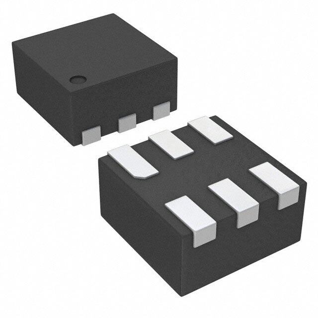
ICGOO电子元器件商城为您提供ISL29102IROZ-T7由Intersil设计生产,在icgoo商城现货销售,并且可以通过原厂、代理商等渠道进行代购。 ISL29102IROZ-T7价格参考¥15.03-¥32.88。IntersilISL29102IROZ-T7封装/规格:光学传感器 - 环境光,IR,UV 传感器, Optical Sensor Ambient 550nm Voltage 6-WDFN Exposed Pad。您可以下载ISL29102IROZ-T7参考资料、Datasheet数据手册功能说明书,资料中有ISL29102IROZ-T7 详细功能的应用电路图电压和使用方法及教程。
| 参数 | 数值 |
| 产品目录 | |
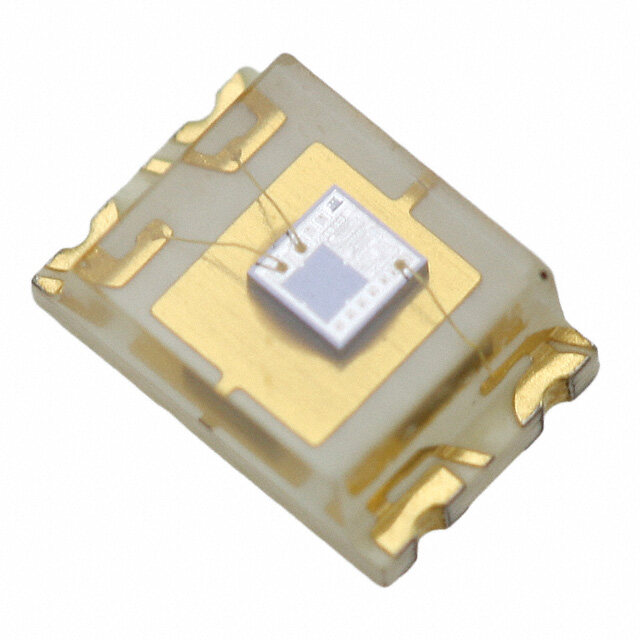
| 描述 | IC OPT SENSOR LIGHT-VOLT 6-ODFN |
| 产品分类 | |
| 品牌 | Intersil |
| 数据手册 | |
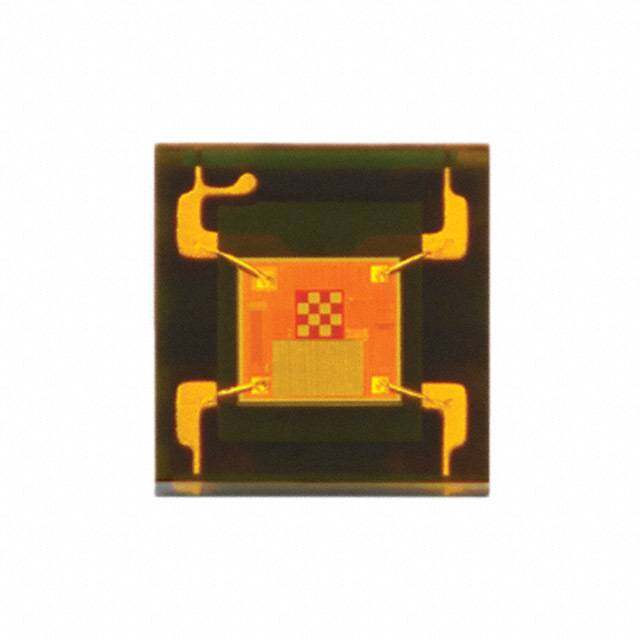
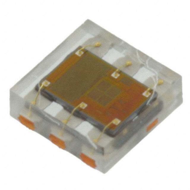
| 产品图片 |
|
| 产品型号 | ISL29102IROZ-T7 |
| rohs | 无铅 / 符合限制有害物质指令(RoHS)规范要求 |
| 产品系列 | - |
| 产品培训模块 | http://www.digikey.cn/PTM/IndividualPTM.page?site=cn&lang=zhs&ptm=12930 |
| 产品目录页面 | |
| 供应商器件封装 | 6-ODFN (2.1x2) |
| 其它名称 | ISL29102IROZ-T7DKR |
| 包装 | Digi-Reel® |
| 安装类型 | 表面贴装 |
| 封装/外壳 | 6-WDFN 裸露焊盘 |
| 工作温度 | -40°C ~ 85°C |
| 带接近传感器 | 无 |
| 标准包装 | 1 |
| 波长 | 550nm |
| 电压-电源 | 1.8 V ~ 3.3 V |
| 类型 | 环境 |
| 输出类型 | 电压 |


- 商务部:美国ITC正式对集成电路等产品启动337调查
- 曝三星4nm工艺存在良率问题 高通将骁龙8 Gen1或转产台积电
- 太阳诱电将投资9.5亿元在常州建新厂生产MLCC 预计2023年完工
- 英特尔发布欧洲新工厂建设计划 深化IDM 2.0 战略
- 台积电先进制程称霸业界 有大客户加持明年业绩稳了
- 达到5530亿美元!SIA预计今年全球半导体销售额将创下新高
- 英特尔拟将自动驾驶子公司Mobileye上市 估值或超500亿美元
- 三星加码芯片和SET,合并消费电子和移动部门,撤换高东真等 CEO
- 三星电子宣布重大人事变动 还合并消费电子和移动部门
- 海关总署:前11个月进口集成电路产品价值2.52万亿元 增长14.8%

PDF Datasheet 数据手册内容提取
DATASHEET ISL29102 FN6483 Low Power Ambient Light-to-Voltage Nonlinear Converter Rev.2.00 Nov 17, 2016 The ISL29102 is a low cost, light-to-voltage silicon optical Features sensor combining a photodiode array, a nonlinear current amplifier, and a micro-power op amp on a single monolithic IC. • Square root voltage output Similar to human eyes, the photodiode array has peak • 0.3 lux to 10,000 lux range sensitivity at 550nm and spans from 400nm to 600nm, • 1.8V to 3.3V supply range rejecting UV light and IR light. The input luminance range is from 0.3 lux to 10,000 lux. • Close to human eye spectral response The integrated nonlinear current amplifier boosts and converts • Fast response time the photodiode signal in a square root fashion, extending the • Internal temperature compensation light input dynamic range, while maintaining excellent • Good IR rejection sensitivity at dim conditions with low lux levels. The device consumes minimal power over a wide range of ambient lux • Low supply current levels because the current consumption ramps at a square • Operating temperature range -40°C to +85°C root fashion. A dark-current compensation circuit minimizes • 6 Ld ODFN: 2mmx2.1mmx0.7mm the effect of temperature-dependent leakage currents in the absence of light, improving the light sensitivity at low lux levels • Pb-free (RoHS compliant) while maintaining excellent sensitivity at low lux levels. The Applications built-in 1µA op amp gives the ISL29102 an output voltage driving advantage for heavier loads. • Display and keypad dimming for: The ISL29102 is housed in an ultra compact 2mmx2.1mm - Mobile devices: smart phone, PDA, GPS ODFN plastic case surface mount package. Operation is rated - Computing devices: notebook PC, webpod from -40°C to +85°C. - Consumer devices: LCD-TV, digital picture frame, digital Related Literature camera • Industrial and medical light sensing • For a full list of related documents, visit our website - ISL29102 product page VDD 1 VOUT - CURRENT 6 LIGHT DATA AMPLIFIER + PROCESS OUTPUT CURRENT LIGHT INTENSITY PHOTODIODE GND ARRAY 2 4 REXT FIGURE 1. SIMPLIFIED BLOCK DIAGRAM FN6483 Rev.2.00 Page 1 of 10 Nov 17, 2016
ISL29102 Ordering Information PART NUMBER TEMP RANGE TAPE AND REEL PACKAGE PKG. (Notes1, 2, 3) (°C) (UNITS) (RoHS COMPLIANT) DWG. # ISL29102IROZ-T7 -40 to +85 3k 6 Ld ODFN L6.2x2.1 ISL29102IROZ-T7A -40 to +85 250 6 Ld ODFN L6.2x2.1 ISL29102IROZ-EVALZ Evaluation Board NOTES: 1. Refer to TB347 for details on reel specifications. 2. These Intersil Pb-free plastic packaged products employ special Pb-free material sets; molding compounds/die attach materials and NiPdAu plate - e4 termination finish, which is RoHS compliant and compatible with both SnPb and Pb-free soldering operations. Intersil Pb-free products are MSL classified at Pb-free peak reflow temperatures that meet or exceed the Pb-free requirements of IPC/JEDEC J STD-020. 3. For Moisture Sensitivity Level (MSL), see the device information page for the ISL29102. For more information on MSL, see techbrief TB363. Pin Configuration ISL29102 (6 LD ODFN) TOP VIEW VDD 1 6 VOUT GND 2 PD 5 NC NC 3 4 REXT Pin Descriptions PIN NUMBER PIN NAME PIN DESCRIPTION 1 VDD Supply (1.8V to 3.3V). 2 GND Ground 3 NC No connect 4 REXT Connected to an external resistor to GND setting the light-to-voltage scaling constant. 5 NC No connect 6 VOUT Voltage Output - PD Thermal pad. The thermal pad can be connected to GND or electrically isolated. FN6483 Rev.2.00 Page 2 of 10 Nov 17, 2016
ISL29102 Absolute Maximum Ratings Thermal Information (TA = +25°C) Supply Voltage Between VDD and GND. . . . . . . . . . . . . . . . . . . . . . . . . .3.6V Thermal Resistance (Typical) JA (°C/W) REXT . . . . . . . . . . . . . . . . . . . . . . . . . . . . . . . . . (-0.5V + GND) to (0.5V + VDD) 6 Ld ODFN (Note4) . . . . . . . . . . . . . . . . . . . . . . . . . . . . . 88 VOUT . . . . . . . . . . . . . . . . . . . . . . . . . . . . . . . . . (-0.5V + GND) to (0.5V + VDD) Maximum Die Temperature . . . . . . . . . . . . . . . . . . . . . . . . . . . . . . . . .+90°C VOUT Short-Circuit Current. . . . . . . . . . . . . . . . . . . . . . . . . . . . . . . . . . <10mA Storage Temperature. . . . . . . . . . . . . . . . . . . . . . . . . . . . . .-40°C to +100°C ESD Rating Operating Temperature . . . . . . . . . . . . . . . . . . . . . . . . . . . . .-40°C to +85°C Human Body Model . . . . . . . . . . . . . . . . . . . . . . . . . . . . . . . . . . . . . . . . 3kV Pb-Free Reflow Profile (*) . . . . . . . . . . . . . . . . . . . . . . . . . . . . . . . see TB477 Machine Model. . . . . . . . . . . . . . . . . . . . . . . . . . . . . . . . . . . . . . . . . . .300V *Peak temperature during solder reflow +235°C max CAUTION: Do not operate at or near the maximum ratings listed for extended periods of time. Exposure to such conditions may adversely impact product reliability and result in failures not covered by warranty. NOTE: 4. JA is measured in free air with the component mounted on a high effective thermal conductivity test board with “direct attach” features. See Tech Brief TB379. Electrical Specifications VDD = 3V, TA = +25°C, REXT = 100kΩ, no load at VOUT, green LED light, unless otherwise specified. MIN MAX SYMBOL PARAMETER TEST CONDITION (Note5) TYP (Note5) UNIT E Range of Input Light Intensity for Square Root 0.3 - 10k Lux Relationship to be Held VDD Operating Supply Voltage 1.8 3.3 V IDD Supply Current E = 0 lux 0.65 µA E = 100 lux 3.5 µA E = 1,000 lux 10 15 µA VOUT0 Light-to-Voltage Accuracy E = 100 lux 0.185 V VOUT1 Light-to-Voltage Accuracy E = 1000 lux 0.460 0.580 0.680 V VDARK Voltage Output in the Absence of Light E = 0 lux, REXT = 10MΩ 20 50 mV VOUT Output Voltage Variation Over Three Light Sources: 10 % Fluorescent, Incandescent, and Halogen PSRR Power Supply Rejection Ratio E = 100 lux, VDD = 1.8V to 3.6V 2.5 mV/V VO-CMPL Maximum Output Compliance Voltage at 95% of VDD-0.7V V Nominal Output VO-MAX Maximum Output Voltage Swing VDD V tR Rise Time E = 0 lux to 300 lux 68 µs E = 0 lux to 1000 lux 68 µs tF Fall Time E = 300 lux to 0 lux 1830 µs E = 1000 lux to 0 lux 970 us tD Delay Time for Rising Edge E = 0 lux to 300 lux 352 µs E = 0 lux to 1000 lux 145 µs tS Delay Time for Falling Edge E = 300 lux to 0 lux 22 µs E = 1000 lux to 0 lux 22 µs ISC Short Circuit Current of Op Amp ±11 mA SR Slew Rate of Op Amp ±10 V/ms VOS Offset Voltage of Op Amp ±1.2 mV NOTE: 5. Compliance to datasheet limits is assured by one or more methods: production test, characterization, and/or design. FN6483 Rev.2.00 Page 3 of 10 Nov 17, 2016
ISL29102 POWER SUPPLY OR SOURCEMETER INPUT LIGHT VDD 10% 90% tR tS 90% tF% ISL29102 VOUT 10% FUNCTION GENERATOR OUTPUT REXT tD FIGURE 2. TEST CIRCUIT FOR RISE/FALL TIME MEASUREMENT FIGURE 3. TIMING DIAGRAM Typical Performance Curves 1.2 1.2 HUMAN EYE RESPONSE Y 1.0 T E SI 1.0 S N ON 0.8 TE SUN P N 0.8 ZED RES 00..46 LIGHT SENSOR RESPONSE D LIGHT I 0.6 HAINLCOAGNEDNESCENT MALI 0.2 LIZE 0.4 FLUORESCENT R A O M N 0.0 OR 0.2 N -0.2 0 300 400 600 800 1.0k 1.1k 300 400 500 600 700 800 900 1000 1100 WAVELENGTH (nm) WAVELENGTH (nm) FIGURE 4. SPECTRAL RESPONSE FIGURE 5. SPECTRUM OF LIGHT SOURCES RADIATION PATTERN 10° 0° 10° 20° 20° LUMINOSITY 30° 30° ANGLE 40° 40° 50° 50° 60° 60° 70° 70° 80° 80° 90° 90° 0.2 0.4 0.6 0.8 1.0 RELATIVE SENSITIVITY FIGURE 6. RADIATION PATTERN FN6483 Rev.2.00 Page 4 of 10 Nov 17, 2016
ISL29102 Typical Performance Curves (Continued) 4.000 0.7 VDD = 3V VDD = 3V 0.6 REXT = 40kΩ HALOGEN REXT = 100kΩ HALOGEN V) 0.400 V) E ( E ( 0.5 G G TA TA 0.4 L L O 0.040 O V V T T 0.3 PU FLUORESCENT PU OUT 0.004 INCANDESCENT OUT 0.2 INCANDESCENT FLUORESCENT 0.1 4x10⁻⁴ 0.0 0.1 1 10 100 1000 10000 0 100 200 300 400 500 600 700 800 900 1000 LIGHT INTENSITY (LUX) LIGHT INTENSITY (LUX) FIGURE 7. OUTPUT VOLTAGE vs LIGHT INTENSITY FIGURE 8. OUTPUT VOLTAGE vs LIGHT INTENSITY 2.0 0.8 1.8 VDD = 3V VDD = 3V HALOGEN 0.7 1.6 REXT = 1MΩ REXT = 1MΩ V) V) 0.6 E ( 1.4 E ( HALOGEN AG 1.2 AG 0.5 T T L L O 1.0 O 0.4 V V T 0.8 T U U 0.3 P FLUORESCENT P T 0.6 T U U 0.2 O 0.4 INCANDESCENT O FLUORESCENT 0.2 0.1 INCANDESCENT 0 0 0 10 20 30 40 50 60 70 80 90 100 0 1 2 3 4 5 6 7 8 9 10 LIGHT INTENSITY (LUX) LIGHT INTENSITY (LUX) FIGURE 9. OUTPUT VOLTAGE vs LIGHT INTENSITY FIGURE 10. OUTPUT VOLTAGE vs LIGHT INTENSITY 1000.00 0.30 FALL TIME 0.25 VDD = 3V 0.025 EQU ANSIENT TIME (ms) 110001...000000 RISE TIME DELAY TIME BEFORE RISING TPUT VOLTAGE (V) 0000....01125050 REXT = 10MΩ 0.005 IVALENT INPUT LIGH R U T T 0.1 O (L 0.00 0.000 U DELAY TIME BEFORE FALLING X ) 0.01 -0.05 1 10 100 1000 -50-40-30-20-10 0 10 20 30 40 50 60 70 80 90 LUX CHANGE FROM/TO 0 LUX (LUX) TEMPERATURE (°C) FIGURE 11. TRANSIENT TIME vs LUX CHANGE FROM/TO 0LUX FIGURE 12. OUTPUT VOLTAGE vs TEMPERATURE AT 0 LUX FN6483 Rev.2.00 Page 5 of 10 Nov 17, 2016
ISL29102 Typical Performance Curves (Continued) 1.10 1.20 VDD = 3V E VDD = 3V G 1.15 FLUORESCENT LIGHT NT (µA) 1.00 RNEOX LTO =A 1D0MΩ T VOLTA 11..0150 E U LY CURR 0.90 ED OUTP 01..9050 1000 LUX 300 LUX P Z UP ALI 0.90 S M 0.80 OR 0.85 N 0.80 -50 -40 -30 -20 -10 0 10 20 30 40 50 60 70 80 90 -50 -40-30 -20 -10 0 10 20 30 40 50 60 70 80 90 TEMPERATURE (°C) TEMPERATURE (°C) FIGURE 13. SUPPLY CURRENT vs TEMPERATURE AT 0 LUX FIGURE 14. NORMALIZED OUTPUT VOLTAGE vs TEMPERATURE 13 1.010 11 VFLDUDO =R 3EVSCENT LIGHT 1000 Lux AGE 1F0L0U0O LRUEXSCENT LIGHT A) LT 1.005 µ O PLY CURRENT ( 597 ZED OUTPUT V 1.000 UP 300 Lux ALI 0.995 S 3 REXT = 100kΩ RM VDD = 3V NO LOAD NO REXT = 100kΩ 1 0.990 -50 -40 -30 -20 -10 0 10 20 30 40 50 60 70 80 90 1.5 2.0 2.5 3.0 3.5 4.0 TEMPERATURE (°C) SUPPLY VOLTAGE (V) FIGURE 15. SUPPLY CURRENT vs TEMPERATURE FIGURE 16. NORMALIZED OUTPUT VOLTAGE vs SUPPLY VOLTAGE 9.6 FLUORESCENT LIGHT LIGHT INTENSITY 1000 Lux VDD = 3V, REXT = 100kΩ T EN 9.4 LIGHT INTENSITY RISES FROM 0 LUX TO 300 LUX R AND FALLS FROM 300 LUX TO 0 LUX WITH WHITE LED R U C Y L P P 9.2 U S VOUT REXT = 100kΩ 0V NO LOAD 9.0 1.5 2.0 2.5 3.0 3.5 4.0 SUPPLY VOLTAGE (V) FIGURE 17. SUPPLY CURRENT vs SUPPLY VOLTAGE FIGURE 18. TRANSIENT RESPONSE OF ISL29102 TO CHANGE IN LIGHT INTENSITY FN6483 Rev.2.00 Page 6 of 10 Nov 17, 2016
ISL29102 Application Information ISL29102's output circuit may result in premature saturation when an excessively large REXT is used. The output compliance Light-to-Voltage Conversion voltage is 700mV below the supply voltage as listed in VO-MAX of the “Electrical Specifications” table on page3. The ISL29102 has responsiveness that is a square-root function of the light intensity intercepted by the photodiode in lux. Optical Sensor Location Outline Because the photodiode has a responsivity that resembles the The green area in Figure19 shows the optical sensor location human eye, conversion rate is independent of the light source outline of ISL29102. Along the pinout direction, the center line (fluorescent light, incandescent light, or direct sunlight). (CL) of the sensor coincides with that of the packaging. The V = ----1---.--8--------A------ ER (EQ. 1) sensor width in this direction is 0.39mm. Perpendicular to the OUT 100lux EXT pinout direction, the CL of the sensor has an 0.19mm offset from the CL of packaging away from pin 1. The sensor width in this In Equation1, VOUT is the output voltage, E is the light intensity, direction is 0.46mm. and REXT is the value of the external resistor. The REXT is used to set the light-to-voltage scaling constant. The compliance of the 2.10mm T E 2.00mm FS F O OR 0.46mm S N E S 0.19mm 0.39mm FIGURE 19. 6 LD ODFN SENSOR LOCATION OUTLINE FN6483 Rev.2.00 Page 7 of 10 Nov 17, 2016
ISL29102 Revision History The revision history provided is for informational purposes only and is believed to be accurate, but not warranted. Please visit our website to make sure you have the latest revision. DATE REVISION CHANGE November 17, 2016 FN6483.2 • Updated datasheet to new standards. • Moved Ordering Information table to page 2. Added ISL29102IROZ-T7A. • Removed Important note above Electrical spec table and added Note 5. • Updated POD from rev 2 to rev 4. Changes were: Added “MAX 0.75” dimension to Side View Changed Note 5 From: Tiebar shown (if present) is a non-functional feature. To: Tiebar shown (if present) is a non-functional feature and maybe located on any of the 4 sides (or ends). Updated Arrows to correct arrow type. December 12, 2008 FN6483.1 Added MSL Note 3 to “Ordering Information” to page2. Corrected Eval board name from ISL29102IROZEVALZ to ISL29102IROZ-EVALZ in “Ordering Information” on page2. Added “Related Literature” on page1 per new data sheet standards. Updated Theta JA in “Thermal Information” on page3 from 90C/W to 88C/W per ASYD in Intrepid. Added Note 4. Revised VO-MAX spec in “Electrical Specifications” table on page3 from: Description: Maximum Output Compliance voltage at 95% of nominal output TYP: VDD - 0.7V To: Description: Maximum Output Voltage Swing TYP: removed (was VDD - 0.7V) MAX: added "VDD" Added new spec to “Electrical Specifications” table on page3 as follows: VO-CMPL Description: Maximum Output Compliance voltage at 95% of nominal output TYP: VDD - 0.7V Updated package outline drawing L6.2x2.1 on page9 to most recent revision. Changes to POD were: Changing the way we dimension the solder pad recommendation on the PODs. Changes inc: Bottom View: Added dimension callouts for solder pad Land Pattern: Added package outline and package outline dimensions. Added lead width of 6x0.30±0.05 and note 4 callout to bottom view Increased the size of the pin 1 shaded area Added “Revision History” on page8 & “Products” on page8 per new data sheet standards. July 1, 2008 FN6483.0 Initial release. FN6483 Rev.2.00 Page 8 of 10 Nov 17, 2016
ISL29102 About Intersil Intersil Corporation is a leading provider of innovative power management and precision analog solutions. The company's products address some of the largest markets within the industrial and infrastructure, mobile computing, and high-end consumer markets. For the most updated datasheet, application notes, related documentation, and related parts, see the respective product information page found at www.intersil.com. You may report errors or suggestions for improving this datasheet by visiting www.intersil.com/ask. Reliability reports are also available from our website at www.intersil.com/support. © Copyright Intersil Americas LLC 2008-2016. All Rights Reserved. All trademarks and registered trademarks are the property of their respective owners. For additional products, see www.intersil.com/en/products.html Intersil products are manufactured, assembled and tested utilizing ISO9001 quality systems as noted in the quality certifications found at www.intersil.com/en/support/qualandreliability.html Intersil products are sold by description only. Intersil may modify the circuit design and/or specifications of products at any time without notice, provided that such modification does not, in Intersil's sole judgment, affect the form, fit or function of the product. Accordingly, the reader is cautioned to verify that datasheets are current before placing orders. Information furnished by Intersil is believed to be accurate and reliable. However, no responsibility is assumed by Intersil or its subsidiaries for its use; nor for any infringements of patents or other rights of third parties which may result from its use. No license is granted by implication or otherwise under any patent or patent rights of Intersil or its subsidiaries. For information regarding Intersil Corporation and its products, see www.intersil.com FN6483 Rev.2.00 Page 9 of 10 Nov 17, 2016
ISL29102 Package Outline Drawing For the most recent package outline drawing, see L6.2x2.1. L6.2x2.1 6 LEAD OPTICAL DUAL FLAT NO-LEAD PLASTIC PACKAGE (ODFN) Rev 4, 2/15 2.10 A 6 B PIN #1 INDEX AREA 6 1 PIN 1 INDEX AREA 0.65 2.00 1.35 1.30 REF 4 6x0.30 ±0.05 (4X) 0.10 0.10 M C A B 0.65 TOP VIEW 6x0.35 ±0.05 BOTTOM VIEW 2.50 PACKAGE OUTLINE 2.10 SEE DETAIL "X" 0.65 0.10 C (4x0.65) MAX 0.75 C BASE PLANE SEATING PLANE 0.08 C SIDE VIEW (1.35) 0.2 REF (6x0.30) (6x0.20) C 5 (6x0.55) 0.00 MIN. 0.05 MAX. TYPICAL RECOMMENDED LAND PATTERN DETAIL "X" NOTES: 1. Dimensions are in millimeters. Dimensions in ( ) for Reference Only. 2. Dimensioning and tolerancing conform to ASME Y14.5m-1994. 3. Unless otherwise specified, tolerance: Decimal ± 0.05 4. Dimension applies to the metallized terminal and is measured between 0.15mm and 0.30mm from the terminal tip. 5. Tiebar shown (if present) is a non-functional feature and maybe located on any of the 4 sides (or ends). 6. The configuration of the pin #1 identifier is optional, but must be located within the zone indicated. The pin #1 identifier may be either a mold or mark feature. FN6483 Rev.2.00 Page 10 of 10 Nov 17, 2016