ICGOO在线商城 > 传感器,变送器 > 光学传感器 - 环境光,IR,UV 传感器 > ISL29003IROZ-T7
- 型号: ISL29003IROZ-T7
- 制造商: Intersil
- 库位|库存: xxxx|xxxx
- 要求:
| 数量阶梯 | 香港交货 | 国内含税 |
| +xxxx | $xxxx | ¥xxxx |
查看当月历史价格
查看今年历史价格
ISL29003IROZ-T7产品简介:
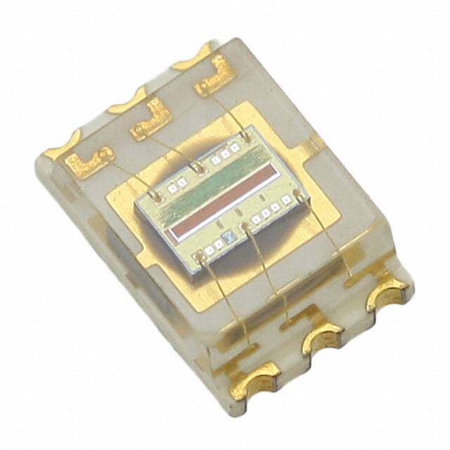
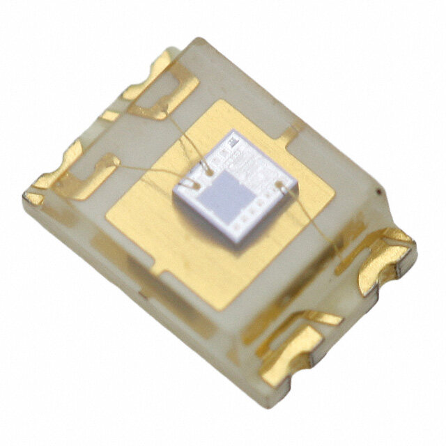
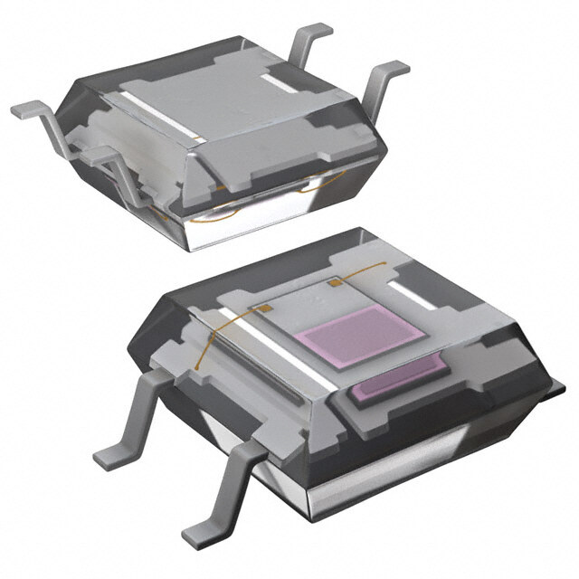
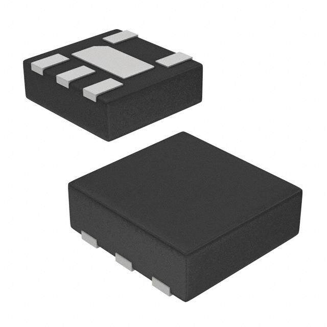
ICGOO电子元器件商城为您提供ISL29003IROZ-T7由Intersil设计生产,在icgoo商城现货销售,并且可以通过原厂、代理商等渠道进行代购。 ISL29003IROZ-T7价格参考¥13.52-¥16.21。IntersilISL29003IROZ-T7封装/规格:光学传感器 - 环境光,IR,UV 传感器, Optical Sensor Ambient 550nm I²C 6-WDFN Exposed Pad。您可以下载ISL29003IROZ-T7参考资料、Datasheet数据手册功能说明书,资料中有ISL29003IROZ-T7 详细功能的应用电路图电压和使用方法及教程。
ISL29003IROZ-T7 是由 Renesas Electronics America Inc. 生产的一款光学传感器,属于环境光、IR(红外)、UV(紫外线)传感器类别。该型号主要用于检测环境光强度,能够为各种应用提供精确的光照测量数据。以下是其主要应用场景:

1. 自动亮度调节:
   ISL29003IROZ-T7 可用于手机、平板电脑、笔记本电脑和显示器等设备中,通过检测环境光强度自动调整屏幕亮度,从而优化用户体验并节省电力。

2. 智能家居系统:
   在智能照明系统中,该传感器可以感知环境光线变化,自动控制灯具的开关或亮度,实现节能和智能化管理。

3. 工业自动化:
   该传感器可用于工业设备中的光照监控,例如生产线上的视觉检测系统,确保设备在适当的光照条件下运行。

4. 健康与可穿戴设备:
   在智能手表、健身追踪器等可穿戴设备中,ISL29003IROZ-T7 可以帮助监测环境光条件,支持更精准的用户界面显示调节。

5. 汽车电子:
   在汽车内部,该传感器可以用于自动调节车内仪表盘和中控屏幕的亮度,提升驾驶安全性与舒适性。

6. 环境监测:
   用于气象站或其他环境监测设备中,测量环境光强、红外或紫外辐射水平,为科学研究或环境保护提供数据支持。

7. 消费电子产品:
   在数码相机、投影仪等设备中,该传感器可以优化图像捕捉或投影效果,根据环境光条件动态调整参数。

ISL29003IROZ-T7 的高灵敏度和低功耗特性使其非常适合需要精确光照测量且对能效要求较高的场景。
| 参数 | 数值 |
| 产品目录 | |
| 描述 | IC SENSOR LIGHT-DGTL I2C 6-ODFN |
| 产品分类 | |
| 品牌 | Intersil |
| 数据手册 | |
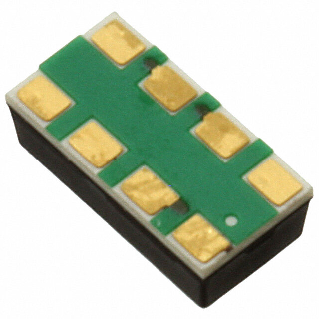
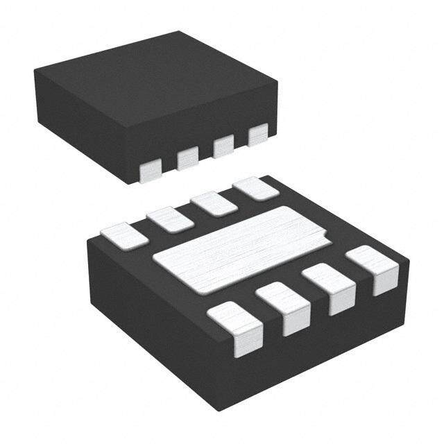
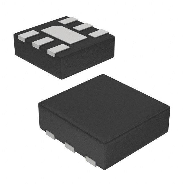
| 产品图片 |
|
| 产品型号 | ISL29003IROZ-T7 |
| rohs | 无铅 / 符合限制有害物质指令(RoHS)规范要求 |
| 产品系列 | - |
| 产品培训模块 | http://www.digikey.cn/PTM/IndividualPTM.page?site=cn&lang=zhs&ptm=12930 |
| 产品目录页面 | |
| 供应商器件封装 | 6-ODFN (2.1x2) |
| 其它名称 | ISL29003IROZ-T7CT |
| 包装 | 剪切带 (CT) |
| 安装类型 | 表面贴装 |
| 封装/外壳 | 6-WDFN 裸露焊盘 |
| 工作温度 | -40°C ~ 85°C |
| 带接近传感器 | 无 |
| 标准包装 | 1 |
| 波长 | 550nm |
| 电压-电源 | 2.5 V ~ 3.3 V |
| 类型 | 环境 |
| 输出类型 | I²C |



- 商务部:美国ITC正式对集成电路等产品启动337调查
- 曝三星4nm工艺存在良率问题 高通将骁龙8 Gen1或转产台积电
- 太阳诱电将投资9.5亿元在常州建新厂生产MLCC 预计2023年完工
- 英特尔发布欧洲新工厂建设计划 深化IDM 2.0 战略
- 台积电先进制程称霸业界 有大客户加持明年业绩稳了
- 达到5530亿美元!SIA预计今年全球半导体销售额将创下新高
- 英特尔拟将自动驾驶子公司Mobileye上市 估值或超500亿美元
- 三星加码芯片和SET,合并消费电子和移动部门,撤换高东真等 CEO
- 三星电子宣布重大人事变动 还合并消费电子和移动部门
- 海关总署:前11个月进口集成电路产品价值2.52万亿元 增长14.8%
PDF Datasheet 数据手册内容提取
ISL29003 ® Data Sheet August 8, 2008 FN7464.5 Light-to-Digital Output Sensor with High Features Sensitivity, Gain Selection, Interrupt 2 • Range select via I2C Function and I C Interface - Range 1 = 0 lux to 1000 lux The ISL29003 is an integrated light sensors with a 16-bit - Range 2 = 0 lux to 4000 lux integrating type ADC, I2C user programmable lux range - Range 3 = 0 lux to 16,000 lux select for optimized counts/lux, and I2C multi-function control - Range 4 = 0 lux to 64,000 lux and monitoring capabilities. The internal ADC provides 16-bit • Human eye response (540nm peak sensitivity) resolution while rejecting 50Hz and 60Hz flicker caused by artificial light sources. • Temperature compensated In normal operation, power consumption is less than 300µA. • 16-bit resolution Furthermore, an available software power-down mode • Adjustable resolution: up to 65 counts per lux controlled via the I2C interface reduces power consumption to less than 1µA. • User-programmable upper and lower threshold interrupt • Simple output code, directly proportional to lux The ISL29003 supports a hardware interrupt that remains asserted low until the host clears it through I2C interface. • IR + UV rejection Designed to operate on supplies from 2.5V to 3.3V, the • 50Hz/60Hz rejection ISL29003 is specified for operation over the -40°C to +85°C • 2.5V to 3.3V supply ambient temperature range. • 6 Ld ODFN (2.1mmx2mm) Ordering Information • Pb-free (RoHS compliant) PART NUMBER PACKAGE Applications (Note) (Pb-free) PKG. DWG. # ISL29003IROZ 6 Ld ODFN L6.2x2.1 • Ambient light sensing ISL29003IROZ-T7* 6 Ld ODFN L6.2x2.1 • Backlight control ISL29003IROZ-EVAL Evaluation Board • Temperature control systems *Please refer to TB347 for details on reel specifications. • Contrast control NOTE: These Intersil Pb-free plastic packaged products employ special Pb-free material sets; molding compounds/die attach • Camera light meters materials and 100% matte tin plate - e3 termination finish, which is RoHS compliant and compatible with both SnPb and Pb-free • Lighting controls soldering operations. Intersil Pb-free products are MSL classified at Pb-free peak reflow temperatures that meet or exceed the Pb-free Pinout requirements of IPC/JEDEC J STD-020. ISL29003 (6 LD ODFN) TOP VIEW Block Diagram VDD VDD 1 6 SDA 1 PHOTODIODE 1 GND 2 THERMAL 5 SCL MODE RANGE NT TIME SHDN COMMAND REXT 3 PAD 4 INT N/ I REGISTER AI MUX G INTEGRATING DATA ADC REGISTER 5 SCL PHOTODIODE 2 EXT I2C 6 SDA TIMING IREF FOSC INT 216 INTERRUPT 4 INT COUNTER 3 2 REXT GND ISL29003 1 CAUTION: These devices are sensitive to electrostatic discharge; follow proper IC Handling Procedures. 1-888-INTERSIL or 1-888-468-3774 | Intersil (and design) is a registered trademark of Intersil Americas Inc. Copyright © Intersil Americas Inc. 2006-2008. All Rights Reserved. All other trademarks mentioned are the property of their respective owners.
ISL29003 Absolute Maximum Ratings (TA = +25°C) Thermal Information VDD Supply Voltage between VDD and GND . . . . . . . . . . . . . 3.6V Maximum Die Temperature . . . . . . . . . . . . . . . . . . . . . . . . . . .+90°C I2C Bus Pin Voltage (SCL, SDA). . . . . . . . . . . . . . . . . -0.2V to 5.5V Storage Temperature. . . . . . . . . . . . . . . . . . . . . . . .-40°C to +100°C I2C Bus Pin Current (SCL, SDA). . . . . . . . . . . . . . . . . . . . . . <10mA Operating Temperature . . . . . . . . . . . . . . . . . . . . . . .-40°C to +85°C INT, REXT Pin Voltage. . . . . . . . . . . . . . . . . . . . . . . . . -0.2V to VDD Pb-free reflow profile . . . . . . . . . . . . . . . . . . . . . . . . . .see link below ESD Rating http://www.intersil.com/pbfree/Pb-FreeReflow.asp Human Body Model . . . . . . . . . . . . . . . . . . . . . . . . . . . . . . . . .2kV CAUTION: Do not operate at or near the maximum ratings listed for extended periods of time. Exposure to such conditions may adversely impact product reliability and result in failures not covered by warranty. IMPORTANT NOTE: All parameters having Min/Max specifications are guaranteed. Typical values are for information purposes only. Unless otherwise noted, all tests are at the specified temperature and are pulsed tests, therefore: TJ = TC = TA Electrical Specifications VDD = 3V, TA = +25°C, REXT = 100kΩ 1% tolerance, unless otherwise specified, Internal Timing Mode operation (See “Principles of Operation” on page3). PARAMETER DESCRIPTION CONDITION MIN TYP MAX UNIT VDD Power Supply Range 2.25 3.3 V IDD Supply Current 0.29 0.33 mA IDD1 Supply Current Disabled Software disabled 0.1 1 µA fOSC1 Internal Oscillator Frequency Gain/Range=1 or 2 290 327 360 kHz fOSC2 Internal Oscillator Frequency Gain/Range=3 or 4 580 655 720 kHz FI2C I2C Clock Rate 1 400 kHz DATA0 Diode1 Dark ADC Code E = 0 lux, Mode1, Gain/Range=1 5 Counts DATA1 Full Scale ADC Code 65535 Counts DATA2 Diode1 ADC Code Gain/Range=1 Accuracy Mode1 E = 300 lux, fluorescent light, 15760 20200 24440 Counts Gain/Range=1 DATA3 Diode2 ADC Code Gain/Range=1 Accuracy Mode2 2020 Counts (Note 1) DATA4 Diode1 ADC Code Gain/Range=2 Accuracy Mode1 E = 300 lux, fluorescent light, 5050 Counts Gain/Range=2 DATA5 Diode2 ADC Code Gain/Range=2 Accuracy Mode2 505 Counts (Note 1) DATA6 Diode1 ADC Code Gain/Range=3 Accuracy Mode1 E = 300 lux, fluorescent light, 1262 Counts Gain/Range=3 DATA5 Diode2 ADC Code Gain/Range=3 Accuracy Mode2 126 Counts (Note 1) DATA6 Diode1 ADC Code Gain/Range=4 Accuracy Mode1 E = 300 lux, fluorescent light, 316 Counts Gain/Range=4 DATA6 Diode2 ADC Code Gain/Range=4 Accuracy Mode2 32 Counts (Note 1) VREF Voltage of REXT Pin 0.485 0.51 0.535 V VTL SCL and SDA Threshold LO (Note 2) 1.05 V VTH SCL and SDA Threshold HI (Note 2) 1.95 V ISDA SDA Current Sinking Capability 3 5 mA IINT INT Current Sinking Capability 3 5 mA NOTES: 1. Fluorescent light is substituted by a white LED during production. 2. The voltage threshold levels of the SDA and SCL pins are VDD dependent: VTL = 0.35*VDD. VTH = 0.65*VDD. 2 FN7464.5 August 8, 2008
ISL29003 Pin Descriptions PIN NUMBER PIN NAME DESCRIPTION 1 VDD Positive supply; connect this pin to a regulated 2.5V to 3.3V supply 2 GND Ground pin. The thermal pad is connected to the GND pin 3 REXT External resistor pin for ADC reference; connect this pin to ground through a (nominal) 100kΩ resistor 4 INT Interrupt pin; LO for interrupt/alarming. The INT pin is an open drain. 5 SCL I2C serial clock The I2C bus lines can be pulled above VDD, 5.5V max. 6 SDA I2C serial data Principles of Operation Interrupt Function The active low interrupt pin is an open drain pull-down Photodiodes configuration. The interrupt pin serves as an alarm or The ISL29003 contains two photodiodes. Diode1 is sensitive monitoring function to determine whether the ambient light to both visible and infrared light, while Diode2 is mostly exceeds the upper threshold or goes below the lower sensitive to infrared light. The spectral response of the two threshold. The user can also configure the persistency of the diodes are independent from one another. See Figure 8 interrupt pin. This eliminates any false triggers, such as Spectral Response vs Wavelength in the performance curves noise or sudden spikes in ambient light conditions. An section. The photodiodes convert light to current. Then, the unexpected camera flash, for example, can be ignored by diodes’ current outputs are converted to digital by a single setting the persistency to 8 integration cycles. built-in integrating type 16-bit Analog-to-Digital Converter (ADC). An I2C command mode determines which photodiode I2C Interface will be converted to a digital signal. Mode1 is Diode1 only. There are eight (8) 8-bit registers available inside the ISL29003. Mode2 is Diode2 only. Mode3 is a sequential Mode1 and The command and control registers define the operation of the Mode2 with an internal subtract function (Diode1 - Diode2). device. The command and control registers do not change until the registers are overwritten.There are two 8-bit registers that Analog-to-Digital Converter (ADC) set the high and low interrupt thresholds. There are four 8-bit The converter is a charge-balancing integrating type 16-bit data Read Only registers; two bytes for the sensor reading and ADC. The chosen method for conversion is best for another two bytes for the timer counts. The data registers converting small current signals in the presence of AC contain the ADC's latest digital output, and the number of clock periodic noise. A 100ms integration time, for instance, highly cycles in the previous integration period. rejects 50Hz and 60Hz power line noise simultaneously. See “Integration Time or Conversion Time” on page8 and “Noise The ISL29003’s I2C interface slave address is hardwired Rejection” on page9. internally as 1000100. When 1000100x with x as R or W is sent after the Start condition, this device compares the first The built-in ADC offers the user flexibility in integration time or seven bits of this byte to its address and matches. conversion time. Two timing modes are available; Internal Timing Mode and External Timing Mode. In Internal Timing Figure 1 shows a sample one-byte read. Figure 2 shows a Mode, integration time is determined by an internal dual speed sample one-byte write. Figure 3 shows a sync_iic timing oscillator (fOSC), and the n-bit (n = 4, 8, 12,16) counter inside diagram sample for externally controlled integration time. the ADC. In External Timing Mode, integration time is The I2C bus master always drives the SCL (clock) line, while determined by the time between two consecutive I2C External either the master or the slave can drive the SDA (data) line. Timing Mode commands. See “External Timing Mode” on Figure 2 shows a sample write. Every I2C transaction begins page7. A good balancing act of integration time and resolution with the master asserting a start condition (SDA falling while depending on the application is required for optimal results. SCL remains high). The following byte is driven by the master and includes the slave address and read/write bit. The ADC has four I2C programmable range select to The receiving device is responsible for pulling SDA low dynamically accommodate various lighting conditions. For during the acknowledgement period. very dim conditions, the ADC can be configured at its lowest range. For very bright conditions, the ADC can be configured Every I2C transaction ends with the master asserting a stop at its highest range. condition (SDA rising while SCL remains high). For more information about the I2C standard, please consult the Philips® I2C specification documents. 3 FN7464.5 August 8, 2008
ISL29003 I2C DATA Start DEVICE ADDRESS W A REGISTER ADDRESS A STOP START DEVICE ADDRESS A DATA BYTE0 A STOP I2C SDA In A6 A5 A4 A3 A2 A1 A0 W A R7 R6 R5 R4 R3 R2 R1 R0 A A6 A5 A4 A3 A2 A1 A0 W A SDA DRIVEN BY ISL29003 NAK I2C SDA Out SDA DRIVEN BY MASTER A SDA DRIVEN BY MASTER A SDA DRIVEN BY MASTER A D7 D6 D5 D4 D3 D2 D1 D0 A I2C CLK 1 2 3 4 5 6 7 8 9 1 2 3 4 5 6 7 8 9 1 2 3 4 5 6 7 8 9 1 2 3 4 5 6 7 8 9 FIGURE 1. I2C READ TIMING DIAGRAM SAMPLE Start DEVICE ADDRESS W A REGISTER ADDRESS A FUNCTIONS A STOP I2C DATA I2C SDA In A6 A5 A4 A3 A2 A1 A0 W A R7 R6 R5 R4 R3 R2 R1 R0 A B7 B6 B5 B4 B3 B2 B1 B0 A I2C SDA Out SDA DRIVEN BY MASTER A SDA DRIVEN BY MASTER A SDA DRIVEN BY MASTER A 1 2 3 4 5 6 7 8 9 1 2 3 4 5 6 7 8 9 1 2 3 4 5 6 7 8 9 I2C CLK In FIGURE 2. I2C WRITE TIMING DIAGRAM SAMPLE Start DEVICE ADDRESS W A REGISTER ADDRESS A Stop I2C DATA I2C SDA In A6 A5 A4 A3 A2 A1 A0 W A R7 R6 R5 R4 R3 R2 R1 R0 A I2C SDA Out SDA DRIVEN BY MASTER A SDA DRIVEN BY MASTER A 1 2 3 4 5 6 7 8 9 1 2 3 4 5 6 7 8 9 I2C CLK In FIGURE 3. I2C sync_iic TIMING DIAGRAM SAMPLE 4 FN7464.5 August 8, 2008
ISL29003 Register Set There are eight registers that are available in the ISL29003. Table 1 summarizes the available registers and their functions. TABLE 1. REGISTER SET ADDR REGISTER (HEX) NAME BIT(S) FUNCTION NAME FUNCTIONS/DESCRIPTION 00 Command 7 Enable 0: disable ADC-core 1: enable ADC-core 6 ADCPD 0: Normal operation 1: Power-down Mode 5 Timing_Mode 0: Integration is internally timed 1: Integration is externally sync/controlled by I2C host 4 Reserved 3:2 Mode<1:0> Selects ADC work mode 0: Diode1’s current to unsigned 16-bit data 1: Diode2’s current to unsigned 16-bit data 2: Difference between diodes (I1 - I2) to signed 15-bit data 3: reserved 1:0 Width<1:0> Number of clock cycles; n-bit resolution 0: 216 cycles 1: 212 cycles 2: 28 cycles 3: 24 cycles 01 Control 7 Ext_Mode Always set to logic 0. Factory use only. 6 Test_Mode Always set to logic 0 5 Int_Flag 0: Interrupt is cleared or not yet triggered 1: Interrupt is triggered 4 Reserved Always set to logic 0. Factory use only. 3:2 Gain<1:0> Selects the gain so range is 0: 0 to 1000 lux 1: 0 to 4000 lux 2: 0 to 16000 lux 3: 0 to 64000 lux 1:0 Int_Persist Interrupt is triggered after <1:0> 0: 1 integration cycle 1: 4 integration cycles 2: 8 integration cycles 3: 16 integration cycles 02 Interrupt Threshold 7:0 Interrupt Threshold High byte of HI interrupt threshold. Default is 0xFF HI HI 03 Interrupt Threshold 7:0 Interrupt Threshold High byte of the LO interrupt threshold. Default is 0x00 LO LO 04 LSB_Sensor 7:0 LSB_Sensor Read-Only data register that contains the least significant byte of the latest sensor reading. 05 MSB_Sensor 7:0 MSB_Sensor Read-Only data register that contains the most significant byte of the latest sensor reading. 06 LSB_Timer 7:0 LSB_Timer Read-Only data register that contains the least significant byte of the timer counter value corresponding to the latest sensor reading. 07 MSB_Timer 7:0 MSB_Timer Read-Only data register that contains the most significant byte of the timer counter value corresponding to the latest sensor reading. 5 FN7464.5 August 8, 2008
ISL29003 TABLE 2. WRITE ONLY REGISTERS At Mode2, the mux directs the current of Diode2 only to the ADC. Mode3 is a sequential Mode1 and Mode2 with REGISTER FUNCTIONS/ an internal subtract function (Diode1 - Diode2). ADDRESS NAME DESCRIPTION TABLE 6. PHOTODIODE SELECT MODE; BITS 2 AND 3 b1xxx_xxxx sync_iic Writing a logic 1 to this address bit ends the current ADC-integration BITS 3:2 MODE and starts another. Used only with 0:0 MODE1. ADC integrates or converts Diode1 only. External Timing Mode. Current is converted to an n-bit unsigned data.* bx1xx_xxxx clar_int Writing a logic 1 to this address bit 0:1 MODE2. ADC integrates or coverts Diode2 only. clears the interrupt. Current is converted to an n-bit unsigned data.* 1:0 MODE3. A sequential MODE1 then MODE2 Command Register 00(hex) operation. The difference current is an (n-1) signed The Read/Write command register has five functions: data.* 1:1 No Operation. 1. Enable; Bit 7. This function either resets the ADC or enables the ADC in normal operation. A logic 0 disables ADC to reset-mode. A logic 1 enables adc to normal *n = 4, 8, 12,16 depending on the number of clock cycles operation. function. TABLE 3. ENABLE 5. Width; Bits 1 and 0. This function determines the number of clock cycles per conversion. Changing the number of BIT 7 OPERATION clock cycles does more than just change the resolution of 0 Disable ADC-Core to Reset-Mode (default) the device; it also changes the integration time, which is the period the device’s analog-to-digital (A/D) converter 1 Enable ADC-Core to Normal Operation samples the photodiode current signal for a lux measurement. 2. ADCPD; Bit 6. This function puts the device in a power-down mode. A logic 0 puts the device in normal TABLE 7. WIDTH operation. A logic 1 powers down the device. BITS 1:0 NUMBER OF CLOCK CYCLES TABLE 4. ADCPD 0:0 216 = 65,536 BIT 6 OPERATION 0:1 212 = 4,096 0 Normal Operation (default) 1:0 28 = 256 1 Power-Down 1:1 24 = 16 Control Register 01(hex) For proper shut down operation, it is recommended to disable ADC first then disable the chip. Specifically, the user The Read/Write control register has three functions: should first send I2C command with Bit 7 = 0 and then send 1. Interrupt flag; Bit 5. This is the status bit of the interrupt. I2C command with Bit 6 = 1. The bit is set to logic high when the interrupt thresholds 3. Timing Mode; Bit 5. This function determines whether the have been triggered, and logic low when not yet integration time is done internally or externally. In Internal triggered. Writing a logic low clears/resets the status bit. Timing Mode, integration time is determined by an TABLE 8. INTERRUPT FLAG internal dual speed oscillator (fOSC), and the n-bit (n = 4, 8, 12,16) counter inside the ADC. In External Timing BIT 5 OPERATION Mode, integration time is determined by the time between 0 Interrupt is cleared or not triggered yet two consecutive external-sync sync_iic pulse commands. 1 Interrupt is triggered TABLE 5. TIMING MODE 2. Range/Gain; Bits 3 and 2. The Full Scale Range can be BIT 5 OPERATION adjusted by an external resistor REXT and/or it can be 0 Internal Timing Mode. Integration time is internally adjusted via I2C using the Gain/Range function. timed determined by fOSC, REXT, and number of Gain/Range has four possible values, Range(k) where k clock cycles. is 1 through 4. Table 9 lists the possible values of 1 External Timing Mode. Integration time is externally Range(k) and the resulting FSR for some typical value timed by the I2C host. REXT resistors. 4. Photodiode Select Mode; Bits 3 and 2. This function controls the mux attached to the two photodiodes. At Mode1, the mux directs the current of Diode1 to the ADC. 6 FN7464.5 August 8, 2008
ISL29003 TABLE 9. RANGE/GAIN TYPICAL FSR LUX RANGES TABLE 11. DATA REGISTERS FSR LUX FSR LUX FSR LUX ADDRESS BITS RANGE@ RANGE@ RANGE@ (hex) CONTENTS 3:2 k RANGE (k) REXT = 100k REXT = 50k REXT = 500k 04 Least-significant byte of most recent sensor reading. 0:0 1 973 973 1946 195 05 Most-significant byte of most recent sensor reading. 0:1 2 3892 3892 7784 778 06 Least-significant byte of timer counter value corresponding to most recent sensor reading. 1:0 3 15,568 15,568 31,136 3114 07 Most-significant byte of timer counter value 1:1 4 62,272 62,272 124,544 12,454 corresponding to most recent sensor reading. 3. Interrupt persist; Bits 1 and 0. The interrupt pin and the Calculating Lux interrupt flag is triggered/set when the data sensor reading is out of the interrupt threshold window after m The ISL29003’s output codes, DATA, are directly consecutive number of integration cycles. The interrupt proportional to lux. persist bits determine m. E = α×DATA (EQ. 1) TABLE 10. INTERRUPT PERSIST The proportionality constant α is determined by the Full BITS 1:0 NUMBER OF INTEGRATION CYCLES Scale Range, FSR, and the n-bit ADC, which is user defined 0:0 1 in the command register. The proportionality constant can also be viewed as the resolution; The smallest lux 0:1 4 measurement the device can measure is α. 1:0 8 FSR α = ------------ (EQ. 2) 1:1 16 n 2 Full Scale Range, FSR, is determined by the software Interrupt Threshold HI Register 02(hex) programmable Range/Gain, Range(k), in the command This register sets the HI threshold for the interrupt pin and register and an external scaling resistor REXT which is the interrupt flag. By default, the Interrupt threshold HI is referenced to 100kΩ. FF(hex). The 8-bit data written to the register represents the upper MSB of a 16-bit value. The LSB is always 00(hex). FSR = Range(k)×-1---0---0----k---Ω---- (EQ. 3) R EXT Interrupt Threshold LO Register 03(hex) The transfer function effectively for each timing mode This register sets the LO threshold for the interrupt pin and becomes: the interrupt flag. By default, the Interrupt threshold LO is 00(hex). The 8-bit data written to the register represents the INTERNAL TIMING MODE upper MSB of a 16-bit value. The LSB is always 00(hex). 100kΩ Range(k)×--R---------------- (EQ. 4) Sensor Data Register 04(hex) and 05(hex) E = -----------------------------------------E----X----T---×DATA n 2 When the device is configured to output a 16-bit data, the least significant byte is accessed at 04(hex), and the most EXTERNAL TIMING MODE significant byte can be accessed at 05(hex). The sensor data 100kΩ register is refreshed after every integration cycle. Range(k)×--R-----E----X---T---- (EQ. 5) E = ----------------------------------------------------×DATA COUNTER Timer Data Register 06(hex) and 07(hex) n = 4, 8, 12, or 16. This is the number of clock cycles Note that the timer counter value is only available when programmed in the command register. using the External Timing Mode. The 06(hex) and 07(hex) are the LSB and MSB respectively of a 16-bit timer counter Range(k) is the user defined range in the Gain/Range bit in value corresponding to the most recent sensor reading. the command register. Each clock cycle increments the counter. At the end of each REXT is an external scaling resistor hardwired to the REXT integration period, the value of this counter is made available pin. over the I2C. This value can be used to eliminate noise introduced by slight timing errors caused by imprecise DATA is the output sensor reading in number of counts external timing. Microcontrollers, for example, often cannot available at the data register. provide high-accuracy command-to-command timing, and 2n represents the maximum number of counts possible in the timer counter value can be used to eliminate the Internal Timing Mode. For the External Timing Mode, the resulting noise. maximum number of counts is stored in the data register named COUNTER. 7 FN7464.5 August 8, 2008
ISL29003 COUNTER is the number increments accrued for between When the Range/Gain bits are set to Range1 or Range2, integration time for External Timing Mode. fOSC runs at half speed compared to when Range/Gain bits are set to Range3 and Range4. Gain/Range, Range (k) 1 (EQ. 8) The Gain/Range can be programmed in the control register fOSC1 = 2---(fOSC2) to give Range (k) determining the FSR. Note that Range(k) is not the FSR (see Equation 3). Range(k) provides four The automatic fOSC adjustment feature allows significant constants depending on programmed k that will be scaled by improvement of signal-to-noise ratio when detecting very low REXT (see Table 9). Unlike REXT, Range(k) dynamically lux signals. adjusts the FSR. This function is especially useful when light Integration Time or Conversion Time conditions are varying drastically while maintaining excellent Integration time is the period during which the device’s resolution. analog-to-digital ADC converter samples the photodiode Number of Clock Cycles, n-bit ADC current signal for a lux measurement. Integration time, in The number of clock cycles determines “n” in the n-bit ADC; 2n other words, is the time to complete the conversion of analog clock cycles is a n-bit ADC. n is programmable in the command photodiode current into a digital signal (number of counts). register in the width function. Depending on the application, a Integration time affects the measurement resolution. For good balance of speed and resolution has to be considered better resolution, use a longer integration time. For short and when deciding for n. For fast and quick measurement, choose fast conversions use a shorter integration time. the smallest n = 4. For maximum resolution without regard of time, choose n = 16. Table 12 compares the trade-off between The ISL29003 offers user flexibility in the integration time to integration time and resolution. See Equations 10 and 11 for the balance resolution, speed and noise rejection. Integration time relation between integration time and n. See Equation 3 for the can be set internally or externally and can be programmed in relation of n and resolution. the command register 00(hex) bit 5. TABLE 12. RESOLUTION AND INTEGRATION TIME INTEGRATION TIME IN INTERNAL TIMING MODE SELECTION This timing mode is programmed in the command register RANGE1 RANGE4 00(hex) bit 5. Most applications will be using this timing fOSC = 327kHz fOSC = 655kHz mode. When using the Internal Timing Mode, fOSC and RESOLUTION RESOLUTION n-bits resolution determine the integration time. tint is a n tINT (ms) LUX/COUNT tINT (ms) (LUX/COUNT) function of the number of clock cycles and fOSC. 16 200 0.01 100 1 tint = 2n×f----1------ for Internal Timing Mode only (EQ. 9) 12 12.8 0.24 6.4 16 osc 8 0.8 3.90 0.4 250 n = 4, 8, 12, and16. n is the number of bits of resolution. 4 0.05 62.5 0.025 4000 Therefore, 2n is the number of clock cycles. n can be REXT = 100kΩ programmed at the command register 00(hex) bits 1 and 0. External Scaling Resistor REXT and fosc Since fOSC is dual speed depending on the Gain/Range bit, The ISL29003 uses an external resistor REXT to fix its tint is dual time. The integration time as a function of REXT and n is: internal oscillator frequency, fOSC. Consequently, REXT R determines the fOSC, integration time and the FSR of the t 1 = 2n×---------------------E----X---T------------------ (EQ. 10) device. fOSC, a dual speed mode oscillator, is inversely int 327kHz×100kΩ proportional to REXT. For user simplicity, the proportionality tint1 is the integration time when the device is configured for constant is referenced to fixed constants 100kΩ and Internal Timing Mode and Gain/Range is set to Range1 or 655kHz: Range2. 1 100kΩ (EQ. 6) fosc1 = 2---×--R-----E---X----T----×655kHz tint2 = 2n×6----5---5----k---H--R---z--E---×-X---T-1---0---0----k----Ω--- (EQ. 11) 100kΩ (EQ. 7) fosc2 = ------------------×655kHz tint2 is the integration time when the device is configured for R EXT Internal Timing Mode and Gain/Range is set to Range3 or Range4. fOSC1 is oscillator frequency when Range1 or Range2 are set. This is nominally 327kHz when REXT is 100kΩ. fOSC2 is the oscillator frequency when Range3 or Range4 are set. This is nominally 655kHz when REXT is 100kΩ. 8 FN7464.5 August 8, 2008
ISL29003 TABLE 13. INTEGRATION TIMES FOR TYPICAL REXT VALUES Noise Rejection In general, integrating type ADC’s have excellent RANGE1 RANGE3 noise-rejection characteristics for periodic noise sources RANGE2 RANGE4 REXT whose frequency is an integer multiple of the integration (kΩ) n = 16-BIT n = 12-BIT n = 12-BIT n = 4 time. For instance, a 60Hz AC unwanted signal’s sum from 50 100 6.4 3.2 0.013 0ms to k*16.66ms (k = 1,2...ki) is zero. Similarly, setting the device’s integration time to be an integer multiple of the 100** 200 13 6.5 0.025 periodic noise signal greatly improves the light sensor output 200 400 26 13 0.050 signal in the presence of noise. 500 1000 64 32 0.125 DESIGN EXAMPLE 1 *Integration time in milliseconds The ISL29003 will be designed in a portable system. The **Recommended REXT resistor value ambient light conditions that the device will be exposed to is INTEGRATION TIME IN EXTERNAL TIMING MODE at most 500 lux, which is a good office lighting. The light source has a 50/60Hz power line noise, which is not visible This timing mode is programmed in the command register by the human eye. The I2C clock is 10kHz. 00(hex) bit 5. External Timing Mode is recommended when integration time can be synchronized to an external signal Solution 1 (such as a PWM) to eliminate noise. Using Internal Timing Mode For Mode1 or Mode2 operation, the integration starts when In order to achieve both 60Hz and 50Hz AC noise rejection, the sync_iic command is sent over the I2C lines. The device the integration time needs to be adjusted to coincide with an needs two sync_iic commands to complete a photodiode integer multiple of the AC noise cycle times. conversion. The integration then stops when another sync_iic command is received. Writing a logic 1 to the t = i(1⁄60Hz)= j(1⁄50Hz) (EQ. 14) int sync_iic bit ends the current ADC integration and starts another one. The first instance of integer values at which tint rejects both 60Hz and 50Hz is when i=6, and j = 5. For Mode3, the operation is a sequential Mode1 and Mode2. t = 6(1⁄60Hz)= 5(1⁄50Hz) The device needs three sync_iic commands to complete two int (EQ. 15) photodiode measurements. The 1st sync_iic command starts t = 100ms int the conversion of the Diode1. The 2nd sync_iic completes the conversion of Diode1 and starts the conversion of Diode2. Next, the Gain/Range needs to be determined. Based on the The 3rd sync_iic pulse ends the conversion of Diode2 and application condition given, lux(max) = 500 lux, a range of starts over again to commence conversion of Diode1. 1000 lux is desirable. This corresponds to a Gain/Range Range1 mode. Also impose a resolution of n = 16-bit. The integration time, tint, is determined by Equation 12: i2 Hence, we choose Equation 10 to determine REXT. I C t = ---------- (EQ. 12) int f2 t ×327kHz×100kΩ I C int R = ------------------------------------------------------------- EXT n 2 iI2C is the number of I2C clock cycles to obtain the tint. (EQ. 16) fI2C is the I2C operating frequency. REXT = 50kΩ The internal oscillator, fOSC, operates identically in both the for Internal Timing Mode and Gain/Range is set to Range3 or Range4 only internal and external timing modes, with the same The Full Scale Range, FSR, needs to be determined from dependence on REXT. However, in External Timing Mode, Equation 3: the number of clock cycles per integration is no longer fixed at 2n. The number of clock cycles varies with the chosen 100kΩ integration time, and is limited to 216 = 65,536. In order to FSR = 1000 lux--5---0----k----Ω----- (EQ. 17) avoid erroneous lux readings, the integration time must be FSR = 2000 lux short enough not to allow an overflow in the counter register. The effective transfer function becomes: 65,535 t <------------------ (EQ. 13) int fOSC E = d-----a---t---a--×2000 lux (EQ. 18) 16 2 fOSC = 327kHz*100kΩ/REXT. When Range/Gain is set to Range1 or Range2. fOSC = 655kHz*100kΩ/REXT. When Range/Gain is set to Range3 or Range4. 9 FN7464.5 August 8, 2008
ISL29003 TABLE 14. SOLUTION1 SUMMARY TO EXAMPLE DESIGN IR Rejection PROBLEM Any filament type light source has a high presence of infrared DESIGN PARAMETER VALUE component invisible to the human eye. A white fluorescent tint 100ms lamp, on the other hand has a low IR content. As a result, output sensitivity may vary depending on the light source. REXT 50kΩ Maximum attenuation of IR can be achieved by properly Gain/Range Mode Range1 = 1000 lux scaling the readings of Diode1 and Diode2. The user obtains FSR 2000 lux data reading from sensor Diode1 (D1), which is sensitive to # of clock cycles 216 visible and IR, then reading from sensor Diode2 (D2), which is mostly sensitive from IR. The graph in Figure 8 shows the Transfer Function DATA E = -----------------×2000 lux effective spectral response after applying Equation 19 of the 16 2 ISL29003 from 400nm to 1000nm. Equation 19 describes the method of cancelling IR in internal timing mode. Solution 2 Using External Timing Mode D3 = n(D1–kD2) (EQ. 19) From Solution 1, the desired integration time is 100ms. Note Where: that the REXT resistor only determines the inter oscillator frequency when using external timing mode. Instead, the data = lux amount in number of counts less IR presence integration time is the time between two sync_iic commands D1 = data reading of Diode1 sent through the I2C. The programmer determines how many I2C clock cycles to wait between two external timing D2 = data reading of Diode2 commands. n = 1.85. This is a fudge factor to scale back the sensitivity iI2C = fI2C*tint = number of I2C clock cycles up to ensure Equation 4 is valid. iI2C = 10kHz *100ms k = 7.5. This is a scaling factor for the IR sensitive Diode2. iI2C = 1,000 I2C clock cycles. An external sync_iic command Flat Window Lens Design sent 1,000 cycles after another sync_iic command rejects A window lens will surely limit the viewing angle of the both 60Hz and 50Hz AC noise signals. ISL29003. The window lens should be placed directly on top of the device. The thickness of the lens should be kept at Next, is to pick an arbitrary REXT = 100kΩ and to choose the minimum to minimize loss of power due to reflection and Gain/Range Mode. For a maximum 500 lux, Range1 is also to minimize loss of loss due to absorption of energy in adequate. From Equation 3: the plastic material. A thickness of t = 1mm is recommended 100kΩ FSR = 1000 lux------------------ for a window lens design. The bigger the diameter of the 100kΩ FSR = 1000 lux window lens, the wider the viewing angle is of the ISL29003. Table 16 shows the recommended dimensions of the optical The effective transfer function becomes: window to ensure both 35° and 45° viewing angle. These DATA E = --------------------------------×1000 lux dimensions are based on a window lens thickness of 1.0mm COUNTER and a refractive index of 1.59. DATA is the sensor reading data located in data registers 04(hex) and 05(hex) WINDOW LENS COUNTER is the timer counter value data located in data registers 06(hex) and 07(hex). In this sample problem, t COUNTER = 1000. DTOTAL ∅ TABLE 15. SOLUTION2 SUMMARY TO EXAMPLE DESIGN D1 PROBLEM DESIGN PARAMETER VALUE tint 100ms REXT 100kΩ ISL29003 DLENS Gain/Range Mode Range1 = 1000 lux FSR 1000 lux ∅ = Viewing angle # of clock cycles COUNTER = 1000 FIGURE 4. FLAT WINDOW LENS Transfer Function DATA E = --------------------------------×1000 lux COUNTER 10 FN7464.5 August 8, 2008
ISL29003 Window with Light Guide Design TABLE 16. RECOMMENDED DIMENSIONS FOR A FLAT If a smaller window is desired while maintaining a wide WINDOW DESIGN effective viewing angle of the ISL29003, a cylindrical piece of DLENS @ 35° DLENS @ 45° transparent plastic is needed to trap the light and then focus DTOTAL D1 VIEWING ANGLE VIEWING ANGLE and guide the light on to the device. Hence, the name light 1.5 0.50 2.25 3.75 guide or also known as light pipe. The pipe should be placed 2.0 1.00 3.00 4.75 directly on top of the device with a distance of D1=0.5mm to achieve peak performance. The light pipe should have 2.5 1.50 3.75 5.75 minimum of 1.5mm in diameter to ensure that whole area of 3.0 2.00 4.30 6.75 the sensor will be exposed. See Figure 5. 3.5 2.50 5.00 7.75 t = 1 Thickness of lens D1 Distance between ISL29001 and inner edge of lens DLENS Diameter of lens DTOTAL Distance constraint between the ISL29001 and lens outer edge *All dimensions are in mm. DLENS D2 >1.5mm LIGHT PIPE t D2 DLENS L ISL29003 FIGURE 5. WINDOW WITH LIGHT GUIDE/PIPE 11 FN7464.5 August 8, 2008
ISL29003 2.10mm 1 6 T 2 5 2.00mm E S F0.29mm OF 0.56mm R O S 3 4 N E S 0.46mm FIGURE 6. SENSOR LOCATION DRAWING Suggested PCB Footprint Typical Circuit Footprint pads should be a nominal 1-to-1 correspondence A typical application for the ISL29003 is shown in Figure 7. with package pads. Since ambient light sensor devices do The ISL29003’s I2C address is internally hardwired as not dissipate high power, heat dissipation through the 1000100. The device can be tied onto a system’s I2C bus exposed pad is not important; instead, similar to DFN or together with other I2C compliant devices. QFN, the exposed pad provides robustness in board mount Soldering Considerations process. Intersil recommends mounting the exposed pad to the PCB, but this is not mandatory. Convection heating is recommended for reflow soldering; direct-infrared heating is not recommended. The plastic Layout Considerations ODFN package does not require a custom reflow soldering The ISL29003 is relatively insensitive to layout. Like other profile, and is qualified to +260°C. A standard reflow I2C devices, it is intended to provide excellent performance soldering profile with a +260°C maximum is recommended. even in significantly noisy environments. There are only a few considerations that will ensure best performance. Route the supply and I2C traces as far as possible from all sources of noise. Use two power-supply decoupling capacitors, 4.7µF and 0.1µF, placed close to the device. 1.8V TO 5.5V R1 R2 R3 I2C MASTER 10k 10k RES1 MICROCONTROLLER SDA SCL 2.5V TO 3.3V I2C SLAVE_0 I2C SLAVE_1 I2C SLAVE_n 1 6 VDD SDA SDA SDA 2 5 SCL SCL GND SCL C1 C2 3 4 4.7µF 0.1µF REXT INT REXT 100k ISL29003 FIGURE 7. ISL29003 TYPICAL CIRCUIT 12 FN7464.5 August 8, 2008
ISL29003 Typical Performance Curves (REXT = 100kΩ) 100 %) 90 RADIATION PATTERN E ( 80 ISL29003 D1 10º 0º 10º S 20º 20º ON 70 LUMANINGOLSEITY 30º 30º P 40º 40º S 60 E D R 50 50º 50º ZE 40 60º 60º LI MA 30 ISL29003 D2 70º 70º R 20 O N 80º 80º 10 0 90º 90º 0.2 0.4 0.6 0.8 1.0 300 400 500 600 700 800 900 1k RELATIVE SENSITIVITY WAVELENGTH (nm) FIGURE 8. SPECTRAL RESPONSE FIGURE 9. RADIATION PATTERN 320 10 TA = +27°C TA = +27°C COMMAND = 00H COMMAND = 00H mA) 306 NTS) 8 0 lux URRENT ( 292 5000 lux ODE (COU 6 PLY C 278 UT C 4 P 200 lux P U T S 264 OU 2 RANGE 2 250 0 2.0 2.3 2.6 2.9 3.2 3.5 3.8 2.0 2.3 2.6 2.9 3.2 3.5 3.8 SUPPLY VOLTAGE (V) SUPPLY VOLTAGE (V) FIGURE 10. SUPPLY CURRENT vs SUPPLY VOLTAGE FIGURE 11. OUTPUT CODE FOR 0 LUX vs SUPPLY VOLTAGE 1.015 320.0 TCAO =M M+2A7N°CD = 00H Hz) TA = +27°C TIO 1.010 CY (k 319.5 A N RV) 5000 lux E DE M 3 1.005 QU UTPUT CO(% FRO 1.000 200 lux ATOR FRE 319.0 O 0.995 CILL 318.5 S O 0.990 318.0 2.0 2.3 2.6 2.9 3.2 3.5 3.8 2.0 2.3 2.6 2.9 3.2 3.5 3.8 SUPPLY VOLTAGE (V) SUPPLY VOLTAGE (V) FIGURE 12. OUTPUT CODE vs SUPPLY VOLTAGE FIGURE 13. OSCILLATOR FREQUENCY vs SUPPLY VOLTAGE 13 FN7464.5 August 8, 2008
ISL29003 Typical Performance Curves (REXT = 100kΩ) (Continued) 315 10 VDD = 3V VDD = 3V COMMAND = 00H COMMAND = 00H T (µA) 305 5000 lux UNTS) 8 0 lux N O RRE 295 RANGE 3 E (C 6 U D C O LY 285 T C 4 P 200 lux U P P U T S 275 RANGE 1 OU 2 RANGE 2 265 0 -60 -20 20 60 100 -60 -20 20 60 100 TEMPERATURE (°C) TEMPERATURE (°C) FIGURE 14. SUPPLY CURRENT vs TEMPERATURE FIGURE 15. OUTPUT CODE FOR 0 LUX vs TEMPERATURE 1.080 330 VDD = 3V z) VDD = 3V COMMAND = 00H H O 1.048 Y (k 329 ATIC) NC OUTPUT CODE R(% FROM +25° 100...099185642 RANGE 35000 lux RANGE2 100 lux CILLATOR FREQUE 333222876 S O 0.920 325 -60 -20 20 60 100 -60 -20 20 60 100 TEMPERATURE (°C) TEMPERATURE (°C) FIGURE 16. OUTPUT CODE vs TEMPERATURE FIGURE 17. OSCILLATOR FREQUENCY vs TEMPERATURE All Intersil U.S. products are manufactured, assembled and tested utilizing ISO9000 quality systems. Intersil Corporation’s quality certifications can be viewed at www.intersil.com/design/quality Intersil products are sold by description only. Intersil Corporation reserves the right to make changes in circuit design, software and/or specifications at any time without notice. Accordingly, the reader is cautioned to verify that data sheets are current before placing orders. Information furnished by Intersil is believed to be accurate and reliable. However, no responsibility is assumed by Intersil or its subsidiaries for its use; nor for any infringements of patents or other rights of third parties which may result from its use. No license is granted by implication or otherwise under any patent or patent rights of Intersil or its subsidiaries. For information regarding Intersil Corporation and its products, see www.intersil.com 14 FN7464.5 August 8, 2008
ISL29003 Package Outline Drawing L6.2x2.1 6 LEAD OPTICAL DUAL FLAT NO-LEAD PLASTIC PACKAGE (ODFN) Rev 0, 9/06 2.10 A 6 PIN 1 INDEX AREA B 1 6 PIN 1 INDEX AREA 0.65 0 1 . 35 1 . 30 REF 0 2. (4X) 0.10 6X 0 . 30 ± 0 . 05 0 . 65 TOP VIEW 0.10M C A B 6X 0 . 35 ± 0 . 05 BOTTOM VIEW (0 . 65) MAX 0.75 SEE DETAIL "X" 0.10 C (0 . 65) (1 . 35) C BASE PLANE SEATING PLANE ( 6X 0 . 30 ) SIDE VIEW 0.08 C ( 6X 0 . 55 ) C 0 . 2 REF 5 (1 . 95) 0 . 00 MIN. 0 . 05 MAX. DETAIL "X" TYPICAL RECOMMENDED LAND PATTERN NOTES: 1. Dimensions are in millimeters. Dimensions in ( ) for Reference Only. 2. Dimensioning and tolerancing conform to AMSE Y14.5m-1994. 3. Unless otherwise specified, tolerance : Decimal ± 0.05 4. Dimension b applies to the metallized terminal and is measured between 0.15mm and 0.30mm from the terminal tip. 5. Tiebar shown (if present) is a non-functional feature. 6. The configuration of the pin #1 identifier is optional, but must be located within the zone indicated. The pin #1 identifier may be either a mold or mark feature. 15 FN7464.5 August 8, 2008

 Datasheet下载

