ICGOO在线商城 > ISL23511UFB8Z
- 型号: ISL23511UFB8Z
- 制造商: Intersil
- 库位|库存: xxxx|xxxx
- 要求:
| 数量阶梯 | 香港交货 | 国内含税 |
| +xxxx | $xxxx | ¥xxxx |
查看当月历史价格
查看今年历史价格
ISL23511UFB8Z产品简介:
ICGOO电子元器件商城为您提供ISL23511UFB8Z由Intersil设计生产,在icgoo商城现货销售,并且可以通过原厂、代理商等渠道进行代购。 提供ISL23511UFB8Z价格参考¥2.69-¥2.69以及IntersilISL23511UFB8Z封装/规格参数等产品信息。 你可以下载ISL23511UFB8Z参考资料、Datasheet数据手册功能说明书, 资料中有ISL23511UFB8Z详细功能的应用电路图电压和使用方法及教程。
| 参数 | 数值 |
| 产品目录 | 集成电路 (IC) |
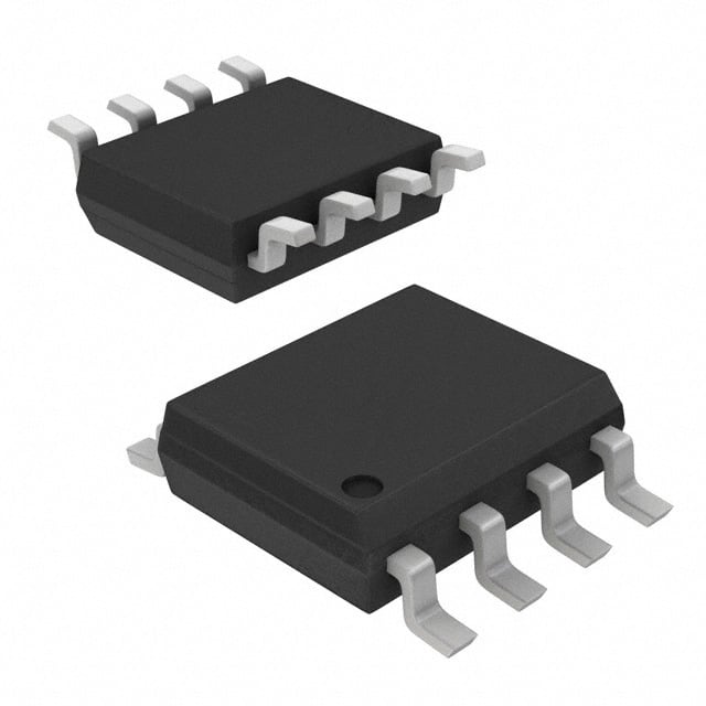
| 描述 | IC POT DGTL PB 32TP LN LP 8-SOIC |
| 产品分类 | |
| 品牌 | Intersil |
| 数据手册 | |
| 产品图片 |
|
| 产品型号 | ISL23511UFB8Z |
| PCN组件/产地 | |
| rohs | 无铅 / 符合限制有害物质指令(RoHS)规范要求 |
| 产品系列 | XDCP™ |
| 供应商器件封装 | 8-SOIC |
| 包装 | 管件 |
| 存储器类型 | 易失 |
| 安装类型 | 表面贴装 |
| 封装/外壳 | 8-SOIC(0.154",3.90mm 宽) |
| 工作温度 | -40°C ~ 125°C |
| 抽头 | 32 |
| 接口 | 2 线按钮 |
| 标准包装 | 980 |
| 温度系数 | 标准值 ±125 ppm/°C |
| 电压-电源 | 2.7 V ~ 5.5 V |
| 电路数 | 1 |
| 电阻(Ω) | 50k |



- 商务部:美国ITC正式对集成电路等产品启动337调查
- 曝三星4nm工艺存在良率问题 高通将骁龙8 Gen1或转产台积电
- 太阳诱电将投资9.5亿元在常州建新厂生产MLCC 预计2023年完工
- 英特尔发布欧洲新工厂建设计划 深化IDM 2.0 战略
- 台积电先进制程称霸业界 有大客户加持明年业绩稳了
- 达到5530亿美元!SIA预计今年全球半导体销售额将创下新高
- 英特尔拟将自动驾驶子公司Mobileye上市 估值或超500亿美元
- 三星加码芯片和SET,合并消费电子和移动部门,撤换高东真等 CEO
- 三星电子宣布重大人事变动 还合并消费电子和移动部门
- 海关总署:前11个月进口集成电路产品价值2.52万亿元 增长14.8%



PDF Datasheet 数据手册内容提取
DATASHEET ISL23511 FN6588 Single Push Button Controlled Potentiometer (XDCP™) Low Noise, Low Power, Rev 2.00 32 Taps, Push Button Controlled Potentiometer September 9, 2015 The Intersil ISL23511 is a three-terminal digitally-controlled Features potentiometer (XDCP) implemented by a resistor array • Solid-state volatile potentiometer composed of 31 resistive elements and a wiper switching network. The ISL23511 features a push button control, a • Push button controlled shutdown mode, as well as an industry-leading µTQFN • Single or Auto increment/decrement package. - Fast Mode after 1s button press The push button control has individual PU and PD inputs for • Shutdown Mode adjusting the wiper. To eliminate redundancy, the wiper position will automatically increment or decrement if one of • 32 wiper tap points these inputs is held longer than 1s. - Zero scale wiper position on power-up Forcing both PU and PD low for more than 2s activates • Low power CMOS shutdown mode. Shutdown mode disconnects the top of the - V = 2.7V to 5.5V CC resistor chain and moves the wiper to the lowest position, - Terminal voltage, 0 to VCC minimizing power consumption. - Standby current, 3µA max The three terminals accessing the resistor chain naturally • R value = 10k50k TOTAL configure the ISL23511 as a voltage divider. A rheostat is • Packages easily formed by floating an end terminal or connecting it to - 8 Ld SOIC and 10 Ld µTQFN (2.1mmx1.6mm) the wiper. VCPCU (SUPPLYCO VNOTRLTOALGE) RH NO VLPPROSUDHNSGER 1234AOV(AITµLOATBPFL10N5E QVOCIRFE SWNUP)P9876ORTENRVRD CWCLC •A•• pPVLEobplD-uflr/mieLceeCa D(CtR ioBoonHrtnigrSosh lctnoemsps liCaonnt)trol PD BLOCK RW NC • Contrast Control O PU 1 8 VCC • Programming Bias Voltages RL PD 2 SOIC 7 NC RH 3(TOP VIEW)6 RL • Ladder Networks VSS 4 5 RW VSS (GROUND) Ordering Information PART PART R TEMP. PACKAGE PKG. TOTAL NUMBER MARKING (k) RANGE (°C) (Pb-free) DWG. # ISL23511WFB8Z* (Note 1) 23511 WFBZ 10 -40 to +125 8 Ld SOIC M8.15 ISL23511WFRU10Z-TK (Note 2) GA 10 -40 to +125 10 Ld µTQFN L10.2.1x1.6A (No longer available or supported) *Add “-TK” suffix for tape and reel. Please refer to TB347 for details on reel specifications. NOTES: 1. These Intersil Pb-free plastic packaged products employ special Pb-free material sets; molding compounds/die attach materials and 100% matte tin plate PLUS ANNEAL - e3 termination finish, which is RoHS compliant and compatible with both SnPb and Pb-free soldering operations. Intersil Pb-free products are MSL classified at Pb-free peak reflow temperatures that meet or exceed the Pb-free requirements of IPC/JEDEC J STD-020. 2. These Intersil Pb-free plastic packaged products employ special Pb-free material sets; molding compounds/die attach materials and NiPdAu plate - e4 termination finish, which is RoHS compliant and compatible with both SnPb and Pb-free soldering operations. Intersil Pb-free products are MSL classified at Pb-free peak reflow temperatures that meet or exceed the Pb-free requirements of IPC/JEDEC J STD-020. FN6588 Rev 2.00 Page 1 of 11 September 9, 2015
ISL23511 Pinouts ISL23511 ISL23511 (8 LD SOIC) (10 LD ΜTQFN) TOP VIEW TOP VIEW NC D O RTE PPUD 12 87 VNCCC PU 1O 10 O R SUP9P O VCC PD 2 BLE 8 NC RH 3 6 RL RH 3 AVAILA 7 RL VSS 4 5 RW VSSN G4ER 6 RW O O L 5 N NC Pin Descriptions SOIC µTQFN PIN PIN SYMBOL BRIEF DESCRIPTION 1 1 PU The PU is a negative-edge triggered input with internal pull-up. Toggling PU will move the wiper close to R H terminal. 2 2 PD The PD is a negative-edge triggered input with internal pull-up. Toggling PD will move the wiper close to R L terminal. 3 3 RH The RH and RL pins of the ISL23511 are equivalent to the fixed terminals of a mechanical potentiometer. The minimum voltage is VSS and the maximum is VCC. The terminology of RH and RL references the relative position of the terminal in relation to wiper movement direction selected by the PU/PD input. 4 4 V Ground SS 5 6 R The R pin is the wiper terminal of the potentiometer, which is equivalent to the movable terminal of a mechanical W W potentiometer. 6 7 RL The RH and RL pins of the ISL23511 are equivalent to the fixed terminals of a mechanical potentiometer. The minimum voltage is VSS and the maximum is VCC. The terminology of RH and RL references the relative position of the terminal in relation to wiper movement direction selected by the PU/PD input. 7 5, 8, 10 NC No connection 8 9 V Supply Voltage CC Block Diagrams 5-BIT 31 RH PU UP/DOWN VCC (SUPPLY VOLTAGE) PD COUNTER 30 29 ONE 28 PU RH OF THIRTY RW CONTROL TWO TRANSFER RESISTOR PD BLOCK RW DECODER GATES ARRAY 2 RL 1 0 VSS (GROUND) RL GENERAL DETAILED FN6588 Rev 2.00 Page 2 of 11 September 9, 2015
ISL23511 Absolute Maximum Ratings Thermal Information Storage Temperature. . . . . . . . . . . . . . . . . . . . . . . .-65°C to +150°C Thermal Resistance (Typical, Note 3, 4) (°C/W) (°C/W) JA JC Voltage at PU and PD Pin with Respect to GND. -0.3V to VCC + 0.3 8 Lead SOIC . . . . . . . . . . . . . . . . . . . . 120 VCC . . . . . . . . . . . . . . . . . . . . . . . . . . . . . . . . . . . . . . . .-0.3V to +6V 10 Lead µTQFN . . . . . . . . . . . . . . . . . 150 48.3 Voltage at any DCP Pin with Respect to GND. . . . . . . .-0.3V to VCC Maximum Junction Temperature (Plastic Package). . . . . . . .+150°C IW (10s) . . . . . . . . . . . . . . . . . . . . . . . . . . . . . . . . . . . . . . . . . . ±6mA Pb-free Reflow Profile . . . . . . . . . . . . . . . . . . . . . . . . .see link below Latchup . . . . . . . . . . . . . . . . . . . . . . . . .Class II, Level A @ +125°C http://www.intersil.com/pbfree/Pb-FreeReflow.asp ESD Rating Human Body Model . . . . . . . . . . . . . . . . . . . . . . . . . . . . . . . . .3kV Recommended Operating Conditions Machine Model. . . . . . . . . . . . . . . . . . . . . . . . . . . . . . . . . . . .250V Temperature Range (Extended Industrial). . . . . . . .-40°C to +125°C V . . . . . . . . . . . . . . . . . . . . . . . . . . . . . . . . . . . . . . . .2.7V to 5.5V CC Power Rating. . . . . . . . . . . . . . . . . . . . . . . . . . . . . . . . . . . . . .15mW Wiper Current . . . . . . . . . . . . . . . . . . . . . . . . . . . . . . . . . . . .±3.0mA CAUTION: Do not operate at or near the maximum ratings listed for extended periods of time. Exposure to such conditions may adversely impact product reliability and result in failures not covered by warranty. NOTES: 3. is measured with the component mounted on a high effective thermal conductivity test board in free air. See Tech Brief TB379 for details. JA 4. For , the “case temp” location is the center of the exposed metal pad on the package underside. JC Potentiometer Specifications Over recommended operating conditions, unless otherwise specified. MIN TYP MAX SYMBOL PARAMETER TEST CONDITIONS (Note 18) (Note5) (Note 18) UNIT R R to R Resistance W option 10 k TOTAL H L U option 50 k R to R Resistance Tolerance -20 +20 % H L End-to-End Temperature Coefficient W option ±80 ppm/°C (Note 16) U option ±125 ppm/°C (Note 16) R Wiper Resistance V = 3.3V, wiper current I = V /R 130 400 W CC RW CC TOTAL V , V V and V Terminal Voltages V and V to GND 0 V V RH RL RH RL RH RL CC Noise on Wiper Terminal From 0Hz to 10MHz -80 dBV C /C /C Potentiometer Capacitance 10/10/25 pF H L W (Note 17) I Leakage on DCP Pins Voltage at pin from GND to V 0.05 0.4 µA LkgDCP CC VOLTAGE DIVIDER MODE (0V @ R ; V @ R ; measured at R unloaded) L CC H W INL Integral Non-linearity -1 1 LSB (Note 10) (Note 6) DNL Differential Non-linearity Monotonic over all tap positions -0.5 0.5 LSB (Note 9) (Note 6) ZSerror Zero-scale Error W option 0 0.3 3 LSB (Note 7) (Note 6) U option 0 0.3 1 FSerror Full-scale Error W option -3 -0.3 0 LSB (Note 8) (Note 6) U option -1 -0.3 0 TC Ratiometric Temperature Coefficient Wiper from 5 hex to 1F hex for W and U ±25 ppm/°C V (Note11) option f 3dB Cut-Off Frequency Wiper at the middle scale, W option 500 kHz CUTOFF Wiper at the middle scale, U option 75 kHz RESISTOR MODE (Measurements between R and R with R not connected, or between R and R with R not connected) W L H W H L RINL Integral Non-linearity DCP register set between 1 hex and 1F hex; -1.5 1.5 MI (Note15) monotonic over all tap positions; W option (Note12) DCP register set between 1 hex and 1F hex; -1 1 MI monotonic over all tap positions; U option (Note12) FN6588 Rev 2.00 Page 3 of 11 September 9, 2015
ISL23511 Potentiometer Specifications Over recommended operating conditions, unless otherwise specified. (Continued) MIN TYP MAX SYMBOL PARAMETER TEST CONDITIONS (Note 18) (Note5) (Note 18) UNIT RDNL Differential Non-linearity W and U option -0.5 0.5 MI (Note14) (Note12) Roffset Offset W option 0 1 3 MI (Note13) (Note12) U option 0 0.5 1 MI (Note12) DC Electrical Specifications Over recommended operating conditions unless otherwise specified. MIN TYP MAX SYMBOL PARAMETER TEST CONDITIONS (Note 18) (Note5) (Note 18) UNIT I V Active Current V = 5.5V, perform wiper move 150 µA CC CC CC operation I Standby Current 0.6 3 µA SB I PU, PD Input Leakage Current V = V to V -2 +2 µA Lkg IN SS CC V PU, PD Input HIGH Voltage V x 0.7 V IH CC V PU, PD input LOW Voltage V x 0.1 V IL CC C PU, PD Input Capacitance V = 3.3V, T =+25°C, f = 1MHz 10 pF IN CC A (Note17) Rpull_up Pull-up Resistor for PU and PD 1 M (Note 17) AC Electrical Specifications Over recommended operating conditions unless otherwise specified. MIN TYP MAX SYMBOL PARAMETER (Note 18) (Note 5) (Note 18) UNIT t Time Between Two Separate Push Button Events 2 ms GAP t Debounce Time 15 30 ms DB t Wiper Change on a Slow Mode 100 250 375 ms S SLOW t Wiper Change on a Fast Mode 25 50 75 ms S FAST t Time to Enter Shutdown Mode (keep PU and PD LOW) 2 s stdn (Note 17) t VCC V Power-up Rate 0.2 50 V/ms R CC NOTES: 5. Typical values are for T = +25°C and 3.3V supply voltage. A 6. LSB: [V(RW) – V(RW) ]/31. V(RW) and V(RW) are voltage on RW pin for the DCP register set to 1F hex and 00 hex respectively. LSB is 31 0 31 0 the incremental voltage when changing from one tap to an adjacent tap. 7. ZS error = V(RW) /LSB. 0 8. FS error = [V(RW) – V ]/LSB. 31 CC 9. DNL = [V(RW) – V(RW) ]/LSB -1, for i = 1 to 31; i is the DCP register setting. i i-1 10. INL = [V(RW) – i • LSB – V(RW)]/LSB for i = 1 to 31 i 11. TC = -------M-----a----x------V-------R-----W--------i-----–-----M-----i--n------V-------R-----W--------i---------------1---0----6-------- for i = 5 to 31 decimal, T = -40°C to +125°C. Max( ) is the maximum value of the wiper V MaxVRW+MinVRW2 +165°Cvoltage and Min ( ) is the minimum value of the wiper voltage over the temperature range. i i 12. MI = |RW – RW |/31. MI is a minimum increment. RW and RW are the measured resistances for the DCP register set to 1F hex and 00 31 0 31 0 hex respectively. 13. Roffset = RW /MI, when measuring between RW and RL. 0 Roffset = RW /MI, when measuring between RW and RH. 31 14. RDNL = (RW – RW )/MI, for i = 1 to 31. i i-1 15. RINL = [RW – (MI • i) – RW ]/MI, for i = 1 to 31. i 0 16. MaxRi–MinRi 106 for i = 5 to 31, T = -40°C to +125°C. Max( ) is the maximum value of the resistance and Min ( ) is TC = ------------------------------------------------------------------------------------- R MaxRi+MinRi2 +165°Cthe minimum value of the resistance over the temperature range. 17. Limits should be considered typical and are not production tested. 18. Parts are 100% tested at +25°C. Over-temperature limits established by characterization and are not production tested. FN6588 Rev 2.00 Page 4 of 11 September 9, 2015
ISL23511 Slow Mode Timing tDB tGAP PU MI* VW * MI in the AC timing diagram refers to the minimum incremental change in the wiper voltage. Fast Mode Timing tDB PU tS FAST tS SLOW MI* VW 1s * MI in the AC timing diagram refers to the minimum incremental change in the wiper voltage. Shutdown Mode Timing tDB 2s SHUTDOWN MODE PU PD VW FN6588 Rev 2.00 Page 5 of 11 September 9, 2015
ISL23511 Typical Performance Curves 160 3.0 VCC = 5.5V 140 +125ºC 2.5 E ()120 C +25ºC 2.0 N100 A A) SIST 80 (µC 1.5 VCC = 5.5V VCC = 2.7V RE 60 IC R 1.0 PE 40 -40ºC WI 0.5 20 0 0 0 5 10 15 20 25 30 -40 -15 10 35 60 85 110 TAP POSITION (DECIMAL) TEMPERATURE (°C) FIGURE 1. WIPER RESISTANCE vs TAP POSITION FIGURE 2. STANDBY I vs TEMPERATURE CC [ I(RW) = V /R ] FOR 10k (W) CC TOTAL 0.010 0.03 VCC = 2.7V 0.02 VCC = 2.7V 0.005 0.01 DNL (LSB) 0.000 INL (LSB)-00..0010 -0.005 -0.02 VCC = 5.5V VCC = 5.5V -0.010 -0.03 0 5 10 15 20 25 30 0 5 10 15 20 25 30 TAP POSITION (DECIMAL) TAP POSITION (DECIMAL) FIGURE 3. DNL vs TAP POSITION IN VOLTAGE DIVIDER FIGURE 4. INL vs TAP POSITION IN VOLTAGE DIVIDER MODE FOR 10k (W) MODE FOR 10k (W) 0 0.006 B) 0.005 SB) -0.1 VCC = 5.5V S L R (L 0.004 OR ( O R -0.2 RR VCC = 5.5V ER LE E 0.003 ALE -0.3 A C RO SC 0.002 VCC = 2.7V ULL S -0.4 ZE 0.001 F VCC = 2.7V -0.5 0 -40 -15 10 35 60 85 110 -40 -15 10 35 60 85 110 TEMPERATURE (°C) TEMPERATURE (°C) FIGURE 5. ZS ERROR vs TEMPERATURE FIGURE 6. FS ERROR vs TEMPERATURE FN6588 Rev 2.00 Page 6 of 11 September 9, 2015
ISL23511 Typical Performance Curves (Continued) 0.2 0.8 VCC = 2.7V VCC = 2.7V 0.1 0.6 RDNL (LSB) 0.0 RINL (LSB) 0.4 VCC = 5.5V -0.1 VCC = 5.5V 0.2 -0.2 0.0 0 5 10 15 20 25 30 0 5 10 15 20 25 30 TAP POSITION (DECIMAL) TAP POSITION (DECIMAL) FIGURE 7. DNL vs TAP POSITION IN RHEOSTAT MODE FOR FIGURE 8. INL vs TAP POSITION IN RHEOSTAT MODE FOR 10k (W) 10k (W) 1.2 40 10k 35 VCC = 5.5V %) 0.6 30 E ( C) 25 NG 10k m/° VCC = 2.7V VCC = 5.5V HA 0.0 pp 20 CTAL TCv ( 15 50k RTO -0.6 VCC = 2.7V 10 50k 5 -1.2 0 -40 -15 10 35 60 85 110 5 10 15 20 25 30 TEMPERATURE (°C) TAP POSITION (DECIMAL) FIGURE 9. END-TO-END R % CHANGE vs FIGURE 10. TC FOR VOLTAGE DIVIDER MODE IN ppm TOTAL TEMPERATURE INPUT SINEWAVE 300 250 50k C)200 pm/°150 VCC = 5.5V 10k p Cr ( MIDSCALE T100 OUTPUT 3dB CUTOFF = 500kHz 50 VCC = 2.7V 0 5 10 15 20 25 30 TAP POSITION (DECIMAL) FIGURE 11. TC FOR RHEOSTAT MODE IN ppm FIGURE 12. FREQUENCY RESPONSE (500kHz) FN6588 Rev 2.00 Page 7 of 11 September 9, 2015
ISL23511 Power-up and Power-down Requirements Internal debounce circuitry prevents inadvertent switching of the wiper position if PU or PD remain LOW for less than 15ms, There are no restrictions on the power-up or power-down typical. Each of the buttons can be pushed either once for a conditions of V and the voltages applied to the CC single increment/decrement or continuously for a multiple potentiometer pins provided that V is always more positive CC increments/decrements. The number of than or equal to V and V , i.e., V V V . The V RH RL CC RH, RL CC increments/decrements of the wiper position depend on how ramp rate specification is always in effect. long the button is being pushed. When making a continuous push, after the first second, the increment/decrement speed Pin Descriptions increases. For the first second, the device will be in the slow R and R scan mode. Then, if the button is held for longer than 1s, the H L device will go into the fast scan mode. As soon as the button is The R and R pins of the ISL23511 are equivalent to the fixed H L released, the ISL23511 will return to a stand-by condition. terminals of a mechanical potentiometer. The minimum voltage is VSS and the maximum is VCC. The terminology of RH and RL If both PU and PD buttons are pulled low more than 15ms from references the relative position of the terminal in relation to each other, all commands are ignored upon release of ALL wiper movement direction. buttons. R W The wiper, when at either fixed terminal, acts like its The R pin is the wiper terminal of the potentiometer which is mechanical equivalent and does not move beyond the last W equivalent to the movable terminal of a mechanical position. That is, the counter does not wrap around when potentiometer. The default wiper position at power-up is at clocked to either extreme. 0tap. Shutdown Mode PU The ISL23511 enters into Shutdown Mode if both PU and PD The debounced PU input is used to increment the wiper inputs are kept LOW for 2s. In this mode, the resistors array is position. An on-chip pull-up holds the PU input HIGH. A switch totally disconnected from its RH pin and the wiper is moved to closure to ground or a LOW logic level will, after a debounce the position closest to the RL pin, as shown in Figure 13. time, move the wiper to the next adjacent higher tap position. RH PD The debounced PD input is used to decrement the wiper position. An on-chip pull-up holds the PD input HIGH. A switch RW closure to ground or a LOW logic level will, after a debounce time, move the wiper to the next adjacent lower tap position. RL Device Operation FIGURE 13. DCP CONNECTION IN SHUTDOWN MODE There are three sections of the ISL23511: the input control, the Note that PU and PD inputs must be brought LOW within t counter and decode section and the resistor array. The input DB time window of 15ms (see “Shutdown Mode Timing” on control section operates just like an up/down counter. The page5) otherwise all commands will be ignored until both output of this counter is decoded to turn on a single electronic inputs are released. switch, connecting a point on the resistor array to the wiper output. The resistor array is comprised of 31 individual Holding either PU or PD input LOW for more than 15ms will resistors connected in series. At either end of the array and exit shutdown mode and return wiper to prior shutdown between each resistor is an electronic switch that transfers the position. If PU or PD will be held LOW for more than 250ms, potential at that point to the wiper. the ISL23511 will start auto-increment or auto-decrement of wiper position. The ISL23511 is designed to interface directly to two push button switches for effectively moving the wiper up or down. R with V Removed TOTAL CC The PU and PD inputs increment or decrement a 5-bit counter The end-to-end resistance of the array will fluctuate once V CC respectively. The output of this counter is decoded to select is removed. one of the thirty-two wiper positions along the resistive array. The wiper increment input, PU and the wiper decrement input, PD are both connected to an internal pull-up so that they normally remain HIGH. When pulled LOW by an external push button switch or a logic LOW level input, the wiper will be switched to the next adjacent tap position. FN6588 Rev 2.00 Page 8 of 11 September 9, 2015
ISL23511 Revision History The revision history provided is for informational purposes only and is believed to be accurate, but not warranted. Please go to the web to make sure that you have the latest revision. DATE REVISION CHANGE September 9, 2015 FN6588.2 - Ordering Information Table on page1. - Added Revision History. - Added About Intersil Verbiage. -Updated POD M8.15 to most current revision with changes as follows: -Revision 1 to Revision 2 Changes: Updated to new POD format by removing table and moving dimensions onto drawing and adding land pattern -Revision 2 to Revision 3 Changes: Changed in Typical Recommended Land Pattern the following: 2.41(0.095) to 2.20(0.087) 0.76 (0.030) to 0.60(0.023) 0.200 to 5.20(0.205) -Revision 3 to Revision 4 Changes: Changed Note 1 "1982" to "1994" About Intersil Intersil Corporation is a leading provider of innovative power management and precision analog solutions. The company's products address some of the largest markets within the industrial and infrastructure, mobile computing and high-end consumer markets. For the most updated datasheet, application notes, related documentation and related parts, please see the respective product information page found at www.intersil.com. You may report errors or suggestions for improving this datasheet by visiting www.intersil.com/ask. Reliability reports are also available from our website at www.intersil.com/support. © Copyright Intersil Americas LLC 2007-2015. All Rights Reserved. All trademarks and registered trademarks are the property of their respective owners. For additional products, see www.intersil.com/en/products.html Intersil products are manufactured, assembled and tested utilizing ISO9001 quality systems as noted in the quality certifications found at www.intersil.com/en/support/qualandreliability.html Intersil products are sold by description only. Intersil may modify the circuit design and/or specifications of products at any time without notice, provided that such modification does not, in Intersil's sole judgment, affect the form, fit or function of the product. Accordingly, the reader is cautioned to verify that datasheets are current before placing orders. Information furnished by Intersil is believed to be accurate and reliable. However, no responsibility is assumed by Intersil or its subsidiaries for its use; nor for any infringements of patents or other rights of third parties which may result from its use. No license is granted by implication or otherwise under any patent or patent rights of Intersil or its subsidiaries. For information regarding Intersil Corporation and its products, see www.intersil.com FN6588 Rev 2.00 Page 9 of 11 September 9, 2015
ISL23511 Ultra Thin Quad Flat No-Lead Plastic Package (UTQFN) L10.2.1x1.6A D A B 10 LEAD ULTRA THIN QUAD FLAT NO-LEAD PLASTIC PACKAGE 6 MILLIMETERS INDEX AREA N E SYMBOL MIN NOMINAL MAX NOTES 2X 0.10 C A 0.45 0.50 0.55 - 1 2 2X 0.10 C A1 - - 0.05 - TOP VIEW A3 0.127 REF - b 0.15 0.20 0.25 5 0.10 C D 2.05 2.10 2.15 - C A 0.05C E 1.55 1.60 1.65 - SEATING PLANE A1 e 0.50 BSC - SIDE VIEW k 0.20 - - - L 0.35 0.40 0.45 - (DATUM A) N 10 2 PIN #1 ID 1 2 4xk Nd 4 3 NX L Ne 1 3 N 0 - 12 4 (DATUM B) Rev. 3 6/06 N-1 NOTES: NX b 5 e 0.10 M CAB 1. Dimensioning and tolerancing conform to ASME Y14.5-1994. 0.05 M C 2. N is the number of terminals. 3 3. Nd and Ne refer to the number of terminals on D and E side, (ND-1) X e respectively. 4. All dimensions are in millimeters. Angles are in degrees. BOTTOM VIEW 5. Dimension b applies to the metallized terminal and is measured between 0.15mm and 0.30mm from the terminal tip. CL 6. The configuration of the pin #1 identifier is optional, but must be NX (b) (A1) located within the zone indicated. The pin #1 identifier may be L either a mold or mark feature. 5 7. Maximum package warpage is 0.05mm. e 8. Maximum allowable burrs is 0.076mm in all directions. SECTION "C-C" 9. Same as JEDEC MO-255UABD except: C C TERMINAL TIP No lead-pull-back, "A" MIN dimension = 0.45 not 0.50mm FOR ODD TERMINAL/SIDE "L" MAX dimension =0.45 not 0.42mm. 10. For additional information, to assist with the PCB Land Pattern Design effort, see Intersil Technical Brief TB389. b 2.50 1.75 0.05 MIN L 2.00 0.80 0.275 0.10 MIN DETAIL “A” PIN 1 ID 0.25 0.50 LAND PATTERN 10 FN6588 Rev 2.00 Page 10 of 11 September 9, 2015
ISL23511 Package Outline Drawing M8.15 8 LEAD NARROW BODY SMALL OUTLINE PLASTIC PACKAGE Rev 4, 1/12 DETAIL "A" 1.27 (0.050) 0.40 (0.016) INDEX 6.20 (0.244) AREA 5.80 (0.228) 0.50 (0.20) x 45° 4.00 (0.157) 0.25 (0.01) 3.80 (0.150) 8° 1 2 3 0° 0.25 (0.010) 0.19 (0.008) TOP VIEW SIDE VIEW “B” 2.20 (0.087) 1 8 SEATING PLANE 0.60 (0.023) 5.00 (0.197) 1.75 (0.069) 2 7 4.80 (0.189) 1.35 (0.053) 1.27 (0.050) 3 6 -C- 4 5 1.27 (0.050) 0.25(0.010) 0.10(0.004) 0.51(0.020) 5.20(0.205) 0.33(0.013) SIDE VIEW “A TYPICAL RECOMMENDED LAND PATTERN NOTES: 1. Dimensioning and tolerancing per ANSI Y14.5M-1994. 2. Package length does not include mold flash, protrusions or gate burrs. Mold flash, protrusion and gate burrs shall not exceed 0.15mm (0.006 inch) per side. 3. Package width does not include interlead flash or protrusions. Interlead flash and protrusions shall not exceed 0.25mm (0.010 inch) per side. 4. The chamfer on the body is optional. If it is not present, a visual index feature must be located within the crosshatched area. 5. Terminal numbers are shown for reference only. 6. The lead width as measured 0.36mm (0.014 inch) or greater above the seating plane, shall not exceed a maximum value of 0.61mm (0.024 inch). 7. Controlling dimension: MILLIMETER. Converted inch dimensions are not necessarily exact. 8. This outline conforms to JEDEC publication MS-012-AA ISSUE C. FN6588 Rev 2.00 Page 11 of 11 September 9, 2015

 Datasheet下载