ICGOO在线商城 > 集成电路(IC) > 时钟/计时 - 实时时钟 > ISL1208IB8Z-T7A

 Datasheet下载
- 型号: ISL1208IB8Z-T7A
- 制造商: Intersil
- 库位|库存: xxxx|xxxx
- 要求:
| 数量阶梯 | 香港交货 | 国内含税 |
| +xxxx | $xxxx | ¥xxxx |
查看当月历史价格
查看今年历史价格
ISL1208IB8Z-T7A产品简介:
ICGOO电子元器件商城为您提供ISL1208IB8Z-T7A由Intersil设计生产,在icgoo商城现货销售,并且可以通过原厂、代理商等渠道进行代购。 ISL1208IB8Z-T7A价格参考。IntersilISL1208IB8Z-T7A封装/规格:时钟/计时 - 实时时钟, Real Time Clock (RTC) IC Clock/Calendar 2B I²C, 2-Wire Serial 8-SOIC (0.154", 3.90mm Width)。您可以下载ISL1208IB8Z-T7A参考资料、Datasheet数据手册功能说明书,资料中有ISL1208IB8Z-T7A 详细功能的应用电路图电压和使用方法及教程。
ISL1208IB8Z-T7A 是由 Renesas Electronics America Inc. 生产的一款实时时钟(RTC)芯片,属于时钟/计时类别。这款器件具有多种应用场景,尤其是在需要精确时间管理的系统中。

 主要应用场景:

1. 消费电子产品:
   - 智能手表和可穿戴设备:ISL1208IB8Z-T7A 提供高精度的时间基准,确保这些设备能够准确显示时间和日期,支持长时间运行而不会显著影响电池寿命。
   - 智能家居设备:如智能音箱、温控器等,需要一个可靠的时钟来同步操作、定时任务和数据记录。

2. 工业自动化:
   - PLC(可编程逻辑控制器):在工业控制系统中,RTC 芯片用于记录事件发生的时间戳,确保系统日志和报警信息的时间准确性。
   - 数据采集系统:用于记录传感器数据的时间戳,便于后续分析和诊断。

3. 医疗设备:
   - 便携式医疗设备:如血糖仪、心率监测仪等,需要精确的时间记录以确保数据的可靠性和合规性。
   - 患者监护系统:RTC 可以帮助记录生命体征数据的时间,确保医生能够准确评估患者的健康状况。

4. 汽车电子:
   - 车载信息系统:如导航系统、娱乐系统等,需要精确的时间管理来提供实时服务和功能。
   - 行车记录仪:记录驾驶过程中发生的事件及其时间,有助于事故分析和责任认定。

5. 通信设备:
   - 路由器和交换机:RTC 用于同步网络设备的时间,确保网络管理和安全功能的正常运作。
   - 基站和无线模块:提供稳定的时间基准,确保通信系统的同步和协调。

6. 嵌入式系统:
   - 物联网(IoT)设备:RTC 芯片为这些设备提供时间基准,支持定时任务、数据同步和远程管理。
   - 低功耗微控制器:在休眠模式下保持时间,唤醒后能立即恢复正确的时间状态。

总之,ISL1208IB8Z-T7A 以其低功耗、高精度和可靠性,在各种需要精确时间管理的应用场景中发挥着重要作用。
| 参数 | 数值 |
| 产品目录 | 集成电路 (IC) |
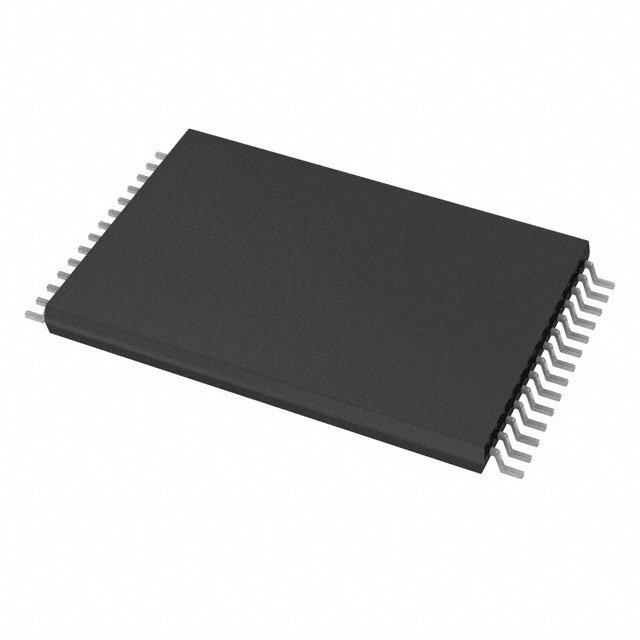
| 描述 | IC RTC CLK/CALENDAR I2C 8-SOIC |
| 产品分类 | |
| 品牌 | Intersil |
| 数据手册 | |
| 产品图片 |
|
| 产品型号 | ISL1208IB8Z-T7A |
| PCN组件/产地 | |
| rohs | 无铅 / 符合限制有害物质指令(RoHS)规范要求 |
| 产品系列 | - |
| 供应商器件封装 | 8-SOIC |
| 其它名称 | ISL1208IB8Z-T7ADKR |
| 包装 | Digi-Reel® |
| 存储容量 | 2B |
| 安装类型 | 表面贴装 |
| 封装/外壳 | 8-SOIC(0.154",3.90mm 宽) |
| 工作温度 | -40°C ~ 85°C |
| 接口 | I²C,2 线串口 |
| 日期格式 | YY-MM-DD-dd |
| 时间格式 | HH:MM:SS(12/24 小时) |
| 标准包装 | 1 |
| 特性 | 警报器,闰年,SRAM |
| 电压-电源 | 2.7 V ~ 5.5 V |
| 电压-电源,电池 | 1.8 V ~ 5.5 V |
| 电流-计时(最大) | 4µA ~ 6µA @ 3V ~ 5V |
| 类型 | 时钟/日历 |


- 商务部:美国ITC正式对集成电路等产品启动337调查
- 曝三星4nm工艺存在良率问题 高通将骁龙8 Gen1或转产台积电
- 太阳诱电将投资9.5亿元在常州建新厂生产MLCC 预计2023年完工
- 英特尔发布欧洲新工厂建设计划 深化IDM 2.0 战略
- 台积电先进制程称霸业界 有大客户加持明年业绩稳了
- 达到5530亿美元!SIA预计今年全球半导体销售额将创下新高
- 英特尔拟将自动驾驶子公司Mobileye上市 估值或超500亿美元
- 三星加码芯片和SET,合并消费电子和移动部门,撤换高东真等 CEO
- 三星电子宣布重大人事变动 还合并消费电子和移动部门
- 海关总署:前11个月进口集成电路产品价值2.52万亿元 增长14.8%


PDF Datasheet 数据手册内容提取
DATASHEET ISL1208 FN8085 2 Rev 8.00 I C Real Time Clock/Calendar, Low Power RTC with Battery Backed SRAM September 12, 2008 The ISL1208 device is a low power real time clock with Features timing and crystal compensation, clock/calendar, power fail • Real Time Clock/Calendar indicator, periodic or polled alarm, intelligent battery backup - Tracks Time in Hours, Minutes, and Seconds switching and battery-backed user SRAM. - Day of the Week, Day, Month, and Year The oscillator uses an external, low-cost 32.768kHz crystal. • 15 Selectable Frequency Outputs The real time clock tracks time with separate registers for hours, minutes, and seconds. The device has calendar • Single Alarm registers for date, month, year and day of the week. The - Settable to the Second, Minute, Hour, Day of the Week, calendar is accurate through 2099, with automatic leap year Day, or Month correction. - Single Event or Pulse Interrupt Mode • Automatic Backup to Battery or Super Capacitor Pinout ISL1208 • Power Failure Detection (8 LD MSOP, SOIC) • On-Chip Oscillator Compensation TOP VIEW • 2 Bytes Battery-Backed User SRAM X1 1 8 VDD • I2C Interface X2 2 7 IRQ/FOUT - 400kHz Data Transfer Rate VBAT 3 6 SCL GND 4 5 SDA • 400nA Battery Supply Current • Same Pin Out as ST M41Txx and Maxim DS13xx Devices ISL1208 • Small Package Options (8 LD TDFN) TOP VIEW - 8 Ld MSOP and SOIC Packages - 8 Ld TDFN Package X1 1 8 VDD • Pb-Free Available (RoHS Compliant) X2 2 7 IRQ/FOUT Applications VBAT 3 6 SCL GND 4 5 SDA • Utility Meters • HVAC Equipment • Audio/Video Components • Set-Top Box/Television • Modems • Network Routers, Hubs, Switches, Bridges • Cellular Infrastructure Equipment • Fixed Broadband Wireless Equipment • Pagers/PDA • POS Equipment • Test Meters/Fixtures • Office Automation (Copiers, Fax) • Home Appliances • Computer Products • Other Industrial/Medical/Automotive FN8085 Rev 8.00 Page 1 of 24 September 12, 2008
ISL1208 .Ordering Information VDD RANGE TEMP. RANGE PART NUMBER PART MARKING (V) (°C) PACKAGE PKG. DWG. # ISL1208IU8 AGS 2.7 to 5.5 -40 to +85 8 Ld MSOP M8.118 ISL1208IU8-TK* AGS 2.7 to 5.5 -40 to +85 8 Ld MSOP Tape and M8.118 Reel ISL1208IU8Z (Note) ANW 2.7 to 5.5 -40 to +85 8 Ld MSOP (Pb-free) M8.118 ISL1208IU8Z-TK* ANW 2.7 to 5.5 -40 to +85 8 Ld MSOP M8.118 (Note) Tape and Reel (Pb-free) ISL1208IB8 1208 I 2.7 to 5.5 -40 to +85 8 Ld SOIC MDP0027 ISL1208IB8-TK* 1208 I 2.7 to 5.5 -40 to +85 8 Ld SOIC Tape and Reel MDP0027 ISL1208IB8Z 1208 ZI 2.7 to 5.5 -40 to +85 8 Ld SOIC (Pb-free) MDP0027 (Note) ISL1208IB8Z-TK* 1208 ZI 2.7 to 5.5 -40 to +85 8 Ld SOIC MDP0027 (Note) Tape andReel (Pb-free) ISL1208IRT8Z 08TZ 2.7 to 5.5 -40 to +85 8 Ld TDFN L8.3x3A (Note) (Pb-free) ISL1208IRT8Z-TK* 08TZ 2.7 to 5.5 -40 to +85 8 Ld TDFN L8.3x3A (Note) Tape and Reel (Pb-free) *Please refer to TB347 for details on reel specifications. NOTE: These Intersil Pb-free plastic packaged products employ special Pb-free material sets, molding compounds/die attach materials, and 100% matte tin plate plus anneal (e3 termination finish, which is RoHS compliant and compatible with both SnPb and Pb-free soldering operations). Intersil Pb-free products are MSL classified at Pb-free peak reflow temperatures that meet or exceed the Pb-free requirements of IPC/JEDEC J STD-020. Block Diagram SDA BUSFDFAER I2C SECONDS SCL SCL INTERFACE CORNTTCROL MINUTES BUFFER LOGIC HOURS DAY OF WEEK X1 CRYSTAL RTC DATE OSCILLATOR DIVIDER X2 MONTH VDD POR FREQUENCY YEAR OUT ALARM CONTROL VTRIP REGISTERS SWITCH USER SRAM IRQ/ VBAT INSTUEPRPNLAYL FOUT FN8085 Rev 8.00 Page 2 of 24 September 12, 2008
ISL1208 Pin Descriptions PIN NUMBER SYMBOL DESCRIPTION 1 X1 The X1 pin is the input of an inverting amplifier and is intended to be connected to one pin of an external 32.768kHz quartz crystal. X1 can also be driven directly from a 32.768kHz source. 2 X2 The X2 pin is the output of an inverting amplifier and is intended to be connected to one pin of an external 32.768kHz quartz crystal. 3 VBAT This input provides a backup supply voltage to the device. VBAT supplies power to the device in the event that the VDD supply fails. This pin should be tied to ground if not used. 4 GND Ground 5 SDA Serial Data (SDA) is a bidirectional pin used to transfer serial data into and out of the device. It has an open drain output and may be wire OR’ed with other open drain or open collector outputs. 6 SCL The Serial Clock (SCL) input is used to clock all serial data into and out of the device. 7 IRQ/FOUT Interrupt Output/Frequency Output is a multi-functional pin that can be used as interrupt or frequency output pin. The function is set via the configuration register. 8 VDD Power supply FN8085 Rev 8.00 Page 3 of 24 September 12, 2008
ISL1208 Absolute Maximum Ratings Thermal Information Voltage on VDD, VBAT, SCL, SDA, and IRQ Pins (Note 3) Thermal Resistance (Typical, Note 1) JA (°C/W) JC (°C/W) (respect to GND) . . . . . . . . . . . . . . . . . . . . . . . . . . . -0.5V to 7.0V SOIC Package. . . . . . . . . . . . . . . . . . . 95 N/A Voltage on X1 and X2 Pins MSOP Package . . . . . . . . . . . . . . . . . . 128 N/A (respect to GND) . . . . . . . . . . . . .-0.5V to VDD + 0.5 (VDD Mode) TDFN Package (Note 2). . . . . . . . . . . . 53.7 2.8 -0.5V to VBAT + 0.5 (VBAT Mode) Storage Temperature. . . . . . . . . . . . . . . . . . . . . . . .-65°C to +150°C Latchup (Note 4) ................Class II, Level B @ +85°C Pb-free Reflow Profile . . . . . . . . . . . . . . . . . . . . . . . . .see link below http://www.intersil.com/pbfree/Pb-FreeReflow.asp CAUTION: Do not operate at or near the maximum ratings listed for extended periods of time. Exposure to such conditions may adversely impact product reliability and result in failures not covered by warranty. NOTES: 1. JA is measured in free air with the component mounted on a high effective thermal conductivity test board with “direct attach” features. See Tech Brief TB379. 2. For JC, the “case temp” location is the center of the exposed metal pad on the package underside. 3. The VDD and SDA pins should not be subjected to negative voltage while the VBAT pin is biased, otherwise latchup can result. See the Applications section. 4. Jedec Class II pulse conditions and failure criterion used. Level B exceptions are using a negative pulse limited to -0.5V. DC Operating Characteristics – RTC Temperature = -40°C to +85°C, unless otherwise stated. MIN TYP MAX SYMBOL PARAMETER CONDITIONS NOTES (Note 9) (Note 8) (Note 9) UNITS VDD Main Power Supply 2.7 5.5 V VBAT Battery Supply Voltage 1.8 5.5 V IDD1 Supply Current VDD = 5V 5, 6 2 6 µA VDD = 3V 1.2 4 µA IDD2 Supply Current With I2C Active VDD = 5V 5, 6 40 120 µA IDD3 Supply Current (Low Power Mode) VDD = 5V, LPMODE = 1 5 1.4 5 µA IBAT Battery Supply Current VBAT = 3V 5 400 950 nA ILI Input Leakage Current on SCL 100 nA ILO I/O Leakage Current on SDA 100 nA VTRIP VBAT Mode Threshold 1.6 2.2 2.6 V VTRIPHYS VTRIP Hysteresis 10 30 75 mV VBATHYS VBAT Hysteresis 15 50 100 mV IRQ/FOUT VOL Output Low Voltage VDD = 5V 0.4 V IOL = 3mA VDD = 2.7V 0.4 V IOL = 1mA Power-Down Timing Temperature = -40°C to +85°C, unless otherwise stated. MIN TYP MAX SYMBOL PARAMETER CONDITIONS NOTES (Note 9) (Note 8) (Note 9) UNITS VDD SR- VDD Negative Slewrate 7 10 V/ms Serial Interface Specifications Over the recommended operating conditions unless otherwise specified. MIN TYP MAX SYMBOL PARAMETER TEST CONDITIONS NOTES (Note 9) (Note 8) (Note 9) UNITS SERIAL INTERFACE SPECS VIL SDA and SCL Input Buffer LOW -0.3 0.3 x V Voltage VDD FN8085 Rev 8.00 Page 4 of 24 September 12, 2008
ISL1208 Serial Interface Specifications Over the recommended operating conditions unless otherwise specified. (Continued) MIN TYP MAX SYMBOL PARAMETER TEST CONDITIONS NOTES (Note 9) (Note 8) (Note 9) UNITS VIH SDA and SCL Input Buffer HIGH 0.7 x VDD + V Voltage VDD 0.3 Hysteresis SDA and SCL Input Buffer 0.05 x V Hysteresis VDD VOL SDA Output Buffer LOW Voltage, 0 0.4 V Sinking 3mA CPIN SDA and SCL Pin Capacitance TA = +25°C, f = 1MHz, VDD = 5V, VIN=0V, 10, 11 10 pF VOUT = 0V fSCL SCL Frequency 400 kHz tIN Pulse width Suppression Time at Any pulse narrower than the max spec is 50 ns SDA and SCL Inputs suppressed. tAA SCL Falling Edge to SDA Output SCL falling edge crossing 30% of VDD, until 900 ns Data Valid SDA exits the 30% to 70% of VDD window. tBUF Time the Bus Must Be Free Before SDA crossing 70% of VDD during a STOP 1300 ns the Start of a New Transmission condition, to SDA crossing 70% of VDD during the following START condition. tLOW Clock LOW Time Measured at the 30% of VDD crossing. 1300 ns tHIGH Clock HIGH Time Measured at the 70% of VDD crossing. 600 ns tSU:STA START Condition Setup Time SCL rising edge to SDA falling edge. Both 600 ns crossing 70% of VDD. tHD:STA START Condition Hold Time From SDA falling edge crossing 30% of VDD 600 ns to SCL falling edge crossing 70% of VDD. tSU:DAT Input Data Setup Time From SDA exiting the 30% to 70% of VDD 100 ns window, to SCL rising edge crossing 30% of VDD tHD:DAT Input Data Hold Time From SCL falling edge crossing 30% of VDD 20 900 ns to SDA entering the 30% to 70% of VDD window. tSU:STO STOP Condition Setup Time From SCL rising edge crossing 70% of VDD, 600 ns to SDA rising edge crossing 30% of VDD. tHD:STO STOP Condition Hold Time From SDA rising edge to SCL falling edge. 600 ns Both crossing 70% of VDD. tDH Output Data Hold Time From SCL falling edge crossing 30% of VDD, 0 ns until SDA enters the 30% to 70% of VDD window. tR SDA and SCL Rise Time From 30% to 70% of VDD 10, 11 20 + 300 ns 0.1xCb tF SDA and SCL Fall Time From 70% to 30% of VDD 10, 11 20 + 300 ns 0.1 x Cb Cb Capacitive Loading of SDA or SCL Total on-chip and off-chip 10, 11 10 400 pF Rpu SDA and SCL Bus Pull-Up Maximum is determined by tR and tF. 10, 11 1 k Resistor Off-Chip For Cb = 400pF, max is about 2kto~2.5k. For Cb = 40pF, max is about 15kto ~20k NOTES: 5. IRQ and FOUT Inactive. 6. LPMODE = 0 (default). 7. In order to ensure proper timekeeping, the VDD SR- specification must be followed. 8. Typical values are for T = +25°C and 3.3V supply voltage. 9. Parameters with MIN and/or MAX limits are 100% tested at +25°C, unless otherwise specified. Temperature limits established by characterization and are not production tested. 10. Parameter is not 100% tested. 11. These are I2C specific parameters and are not tested, however, they are used to set conditions for testing devices to validate specification. FN8085 Rev 8.00 Page 5 of 24 September 12, 2008
ISL1208 SDA vs SCL Timing tF tHIGH tLOW tR SCL tSU:DAT tSU:STA tHD:DAT tSU:STO tHD:STA SDA (INPUT TIMING) tAA tDH tBUF SDA (OUTPUT TIMING) Symbol Table WAVEFORM INPUTS OUTPUTS Must be steady Will be steady May change Will change from LOW from LOW to HIGH to HIGH May change Will change from HIGH from HIGH to LOW to LOW Don’t Care: Changing: Changes Allowed State Not Known N/A Center Line is High Impedance FN8085 Rev 8.00 Page 6 of 24 September 12, 2008
ISL1208 Typical Performance Curves Temperature is +25°C unless otherwise specified 1E-6 1E-6 900E-9 800E-9 800E-9 700E-9 I (A)BAT 456000000EEE---999 I (A)BAT 460000EE--99 300E-9 200E-9 200E-9 100E-9 000E+0 000E+0 1.5 2.0 2.5 3.0 3.5 4.0 4.5 5.0 5.5 -40 -20 0 20 40 60 80 VBAT (V) TEMPERATURE (°C) FIGURE 1. IBAT vs VBAT FIGURE 2. IBAT vs TEMPERATURE AT VBAT = 3V 2.4E-06 2.4E-6 2.2E-6 2.2E-06 VCC= 5V 2.0E-6 2.0E-06 1.8E-6 LPMODE = 0 (A)1 1.8E-06 (A)D1 11..46EE--66 LPMODE = 1 DD 1.6E-06 ID 1.2E-6 I VCC= 3.3V 1.0E-6 1.4E-06 800.0E-9 1.2E-06 600.0E-9 1.0E-06 400.0E-9 -40 -20 0 20 40 60 80 2.5 3.0 3.5 4.0 4.5 5.0 5.5 TEMPERATURE (°C) VCC (V) FIGURE 3. IDD1 vs TEMPERATURE FIGURE 4. IDD1 vs VCC WITH LPMODE ON AND OFF 2.1E-6 3.0E-6 2.9E-6 2.0E-6 2.8E-6 1.9E-6 2.7E-6 1.8E-6 2.6E-6 (A)D1 1.7E-6 (A)1 22..45EE--66 D 1.6E-6 D I D 2.3E-6 I 1.5E-6 2.2E-6 2.1E-6 1.4E-6 2.0E-6 1.3E-6 1.9E-6 1.2E-6 1.8E-6 2 6 8 4 2 1 2 4 8 6 2 4 4 6 8 2 6 8 4 2 1 2 4 8 6 2 4 4 6 8 1/3 1/1 1/ 1/ 1/FOUT (Hz) 1 3 6 102 409 276 1/3 1/1 1/ 1/ 1/ FOUT (Hz) 1 3 6 102 409 276 3 3 FIGURE 5. IDD1 vs FOUT AT VDD = 3.3V FIGURE 6. IDD1 vs FOUT AT VDD = 5V FN8085 Rev 8.00 Page 7 of 24 September 12, 2008
ISL1208 EQUIVALENT AC OUTPUT LOAD CIRCUIT FOR VDD = 5V 5.0V X1 FOR VOL= 0.4V X2 1533 SDA AND IOL = 3mA AND IRQ/fOUT FIGURE 8. RECOMMENDED CRYSTAL CONNECTION 100pF V BAT This input provides a backup supply voltage to the device. FIGURE 7. STANDARD OUTPUT LOAD FOR TESTING THE DEVICE WITH VDD = 5.0V VBAT supplies power to the device in the event that the VDD supply fails. This pin can be connected to a battery, a Super General Description Cap or tied to ground if not used. The ISL1208 device is a low power real time clock with timing IRQ/fOUT (Interrupt Output/Frequency Output) and crystal compensation, clock/calendar, power fail indicator, This dual function pin can be used as an interrupt or frequency periodic or polled alarm, intelligent battery backup switching, output pin. The IRQ/FOUT mode is selected via the frequency and battery-backed user SRAM. out control bits of the control/status register. The oscillator uses an external, low-cost 32.768kHz crystal. • Interrupt Mode. The pin provides an interrupt signal output. The real time clock tracks time with separate registers for This signal notifies a host processor that an alarm has hours, minutes, and seconds. The device has calendar occurred and requests action. It is an open drain active low registers for date, month, year and day of the week. The output. calendar is accurate through 2099, with automatic leap year • Frequency Output Mode. The pin outputs a clock signal correction. which is related to the crystal frequency. The frequency The ISL1208's powerful alarm can be set to any clock/calendar output is user selectable and enabled via the I2C bus. It is an value for a match. For example, every minute, every Tuesday open drain active low output. or at 5:23 AM on March 21. The alarm status is available by Serial Clock (SCL) checking the Status Register, or the device can be configured The SCL input is used to clock all serial data into and out of the to provide a hardware interrupt via the IRQ pin. There is a device. The input buffer on this pin is always active (not gated). repeat mode for the alarm allowing a periodic interrupt every minute, every hour, every day, etc. It is disabled when the backup power supply on the VBAT pin is activated to minimize power consumption. The device also offers a backup power input pin. This VBAT pin Serial Data (SDA) allows the device to be backed up by battery or Super Capacitor with automatic switchover from VDD to VBAT. The SDA is a bidirectional pin used to transfer data into and out of entire ISL1208 device is fully operational from 2.0V to 5.5V and the device. It has an open drain output and may be ORed with the clock/calendar portion of the device remains fully other open drain or open collector outputs. The input buffer is operational down to 1.8V (Standby Mode). always active (not gated) in normal mode. An open drain output requires the use of a pull-up resistor. The Pin Description output circuitry controls the fall time of the output signal with X1, X2 the use of a slope controlled pull-down. The circuit is designed for 400kHz I2C interface speeds. It is disabled when the The X1 and X2 pins are the input and output, respectively, of backup power supply on the VBAT pin is activated. an inverting amplifier. An external 32.768kHz quartz crystal is used with the ISL1208 to supply a timebase for the real time V , GND DD clock. Internal compensation circuitry provides high accuracy Chip power supply and ground pins. The device will operate over the operating temperature range from -40°Cto +85°C. with a power supply from 2.0V to 5.5VDC. A 0.1µF capacitor is This oscillator compensation network can be used to calibrate recommended on the VDD pin to ground. the crystal timing accuracy over temperature either during manufacturing or with an external temperature sensor and Functional Description microcontroller for active compensation. The device can also be driven directly from a 32.768kHz source at pin X1. Power Control Operation The power control circuit accepts a VDD and a VBAT input. Many types of batteries can be used with Intersil RTC products. For example, 3.0V or 3.6V Lithium batteries are appropriate, and battery sizes are available that can power the FN8085 Rev 8.00 Page 8 of 24 September 12, 2008
ISL1208 ISL1208 for up to 10 years. Another option is to use a Super The I2C bus is deactivated in battery backup mode to provide Cap for applications where VDD is interrupted for up to a lower power. Aside from this, all RTC functions are operational month. See the “Application Section” on page18 for more during battery backup mode. Except for SCL and SDA, all the information. inputs and outputs of the ISL1208 are active during battery backup mode unless disabled via the control register. The User Normal Mode (V ) to Battery Backup Mode (V ) DD BAT SRAM is operational in battery backup mode down to 2V. To transition from the VDD to VBAT mode, both of the following Power Failure Detection conditions must be met: The ISL1208 provides a Real Time Clock Failure Bit (RTCF) to Condition 1: detect total power failure. It allows users to determine if the VDD < VBAT - VBATHYS device has powered up after having lost all power to the device where VBATHYS 50mV (both VDD and VBAT). Condition 2: Low Power Mode VDD < VTRIP where VTRIP 2.2V The normal power switching of the ISL1208 is designed to Battery Backup Mode (V ) to Normal Mode (V ) switch into battery backup mode only if the VDD power is lost. BAT DD This will ensure that the device can accept a wide range of The ISL1208 device will switch from the VBAT to VDD mode backup voltages from many types of sources while reliably when one of the following conditions occurs: switching into backup mode. Another mode, called Low Power Condition 1: Mode, is available to allow direct switching from VDD to VBAT VDD > VBAT + VBATHYS without requiring VDD to drop below VTRIP. Since the where VBATHYS 50mV additional monitoring of VDD vs VTRIP is no longer needed, that circuitry is shut down and less power is used while Condition 2: operating from VDD. Power savings are typically 600nA at VDD VDD > VTRIP + VTRIPHYS = 5V. Low Power Mode is activated via the LPMODE bit in the where VTRIPHYS 30mV control and status registers. These power control situations are illustrated in Figures 9 and Low Power Mode is useful in systems where VDD is normally 10. higher than VBAT at all times. The device will switch from VDD to VBAT when VDD drops below VBAT, with about 50mV of hysteresis to prevent any switchback of VDD after switchover. BATTERY BACKUP In a system with a VDD = 5V and backup lithium battery of MODE VDD VBAT = 3V, Low Power Mode can be used. However, it is not recommended to use Low Power Mode in a system with VDD = VTRIP 2.2V 3.3V ±10%, VBAT 3.0V, and when there is a finite I-R voltage VBAT 1.8V drop in the VDD line. VBAT - VBATHYS VBAT + VBATHYS InterSeal™ Battery Saver The ISL1208 has the InterSeal™ Battery Saver which prevents initial battery current drain before it is first used. For example, FIGURE 9. BATTERY SWITCHOVER WHEN VBAT < VTRIP battery-backed RTCs are commonly packaged on a board with a battery connected. In order to preserve battery life, the ISL1208 will not draw any power from the battery source until after the device is first powered up from the VDD source. Thereafter, the device will switchover to battery backup mode BATTERY BACKUP whenever VDD power is lost. MODE VDD Real Time Clock Operation VBAT 3.0V The Real Time Clock (RTC) uses an external 32.768kHz quartz crystal to maintain an accurate internal representation of second, VTRIP 2.2V minute, hour, day of week, date, month, and year. The RTC also has leap-year correction. The clock also corrects for months VTRIP VTRIP + VTRIPHYS having fewer than 31 days and has a bit that controls 24-hour or AM/PM format. When the ISL1208 powers up after the loss of FIGURE 10. BATTERY SWITCHOVER WHEN VBAT > VTRIP both VDD and VBAT, the clock will not begin incrementing until at least one byte is written to the clock register. FN8085 Rev 8.00 Page 9 of 24 September 12, 2008
ISL1208 2 Accuracy of the Real Time Clock I C Serial Interface The accuracy of the Real Time Clock depends on the The ISL1208 has an I2C serial bus interface that provides frequency of the quartz crystal that is used as the time base for access to the control and status registers and the user SRAM. the RTC. Since the resonant frequency of a crystal is The I2C serial interface is compatible with other industry I2C temperature dependent, the RTC performance will also be serial bus protocols using a bidirectional data signal (SDA) and dependent upon temperature. The frequency deviation of the a clock signal (SCL). crystal is a function of the turnover temperature of the crystal Oscillator Compensation from the crystal’s nominal frequency. For example, a ~20ppm frequency deviation translates into an accuracy of ~1 minute The ISL1208 provides the option of timing correction due to per month. These parameters are available from the crystal temperature variation of the crystal oscillator for either manufacturer. The ISL1208 provides on-chip crystal manufacturing calibration or active calibration. The total compensation networks to adjust load capacitance to tune possible compensation is typically -94ppm to +140ppm. Two oscillator frequency from -94ppm to +140ppm. For more compensation mechanisms that are available are as follows: detailed information. See “Application Section” on page18. 1. An analog trimming (ATR) register that can be used to adjust individual on-chip digital capacitors for oscillator Single Event and Interrupt capacitance trimming. The individual digital capacitor is The alarm mode is enabled via the ALME bit. Choosing single selectable from a range of 9pF to 40.5pF (based upon event or interrupt alarm mode is selected via the IM bit. Note 32.758kHz). This translates to a calculated compensation that when the frequency output function is enabled, the alarm of approximately -34ppm to +80ppm. (See ATR description function is disabled. on page18). 2. A digital trimming register (DTR) that can be used to adjust The standard alarm allows for alarms of time, date, day of the the timing counter by ±60ppm. (See DTR description on week, month, and year. When a time alarm occurs in single page18). event mode, an IRQ pin will be pulled low and the alarm status bit (ALM) will be set to “1”. Also provided is the ability to adjust the crystal capacitance when the ISL1208 switches from VDD to battery backup mode. The pulsed interrupt mode allows for repetitive or recurring See “Battery Backup Mode (VBAT) to Normal Mode (VDD)” on alarm functionality. Hence, once the alarm is set, the device page9. will continue to alarm for each occurring match of the alarm and present time. Thus, it will alarm as often as every minute (if Register Descriptions only the nth second is set) or as infrequently as once a year (if The battery-backed registers are accessible following a slave at least the nth month is set). During pulsed interrupt mode, the byte of “1101111x” and reads or writes to addresses [00h:13h]. IRQ pin will be pulled low for 250ms and the alarm status bit The defined addresses and default values are described in (ALM) will be set to “1”. Table 1. Address 09h is not used. Reads or writes to 09h will NOTE: The ALM bit can be reset by the user or cleared automatically not affect operation of the device but should be avoided. using the auto reset mode (see ARST bit). REGISTER ACCESS The alarm function can be enabled/disabled during battery backup mode using the FOBATB bit. For more information on The contents of the registers can be modified by performing a the alarm, See “Alarm Registers” on page14. byte or a page write operation directly to any register address. Frequency Output Mode The registers are divided into 4 sections. These are: The ISL1208 has the option to provide a frequency output 1. Real Time Clock (7 bytes): Address 00h to 06h. signal using the IRQ/FOUT pin. The frequency output mode is 2. Control and Status (5 bytes): Address 07h to 0Bh. set by using the FO bits to select 15 possible output frequency 3. Alarm (6 bytes): Address 0Ch to 11h. values from 0kHz to 32kHz. The frequency output can be 4. User SRAM (2 bytes): Address 12h to 13h. enabled/disabled during battery backup mode using the FOBATB bit. There are no addresses above 13h. General Purpose User SRAM The ISL1208 provides 2 bytes of user SRAM. The SRAM will continue to operate in battery backup mode. However, it should be noted that the I2C bus is disabled in battery backup mode. FN8085 Rev 8.00 Page 10 of 24 September 12, 2008
ISL1208 Write capability is allowable into the RTC registers (00h to 06h) instruction latches all clock registers into a buffer, so an update only when the WRTC bit (bit 4 of address 07h) is set to “1”. A of the clock does not change the time being read. A sequential multi-byte read or write operation is limited to one section read will not result in the output of data from the memory array. per operation. Access to another section requires a new At the end of a read, the master supplies a stop condition to operation. A read or write can begin at any address within the end the operation and free the bus. After a read, the address section. remains at the previous address +1 so the user can execute a current address read and continue reading the next register. A register can be read by performing a random read at any address at any time. This returns the contents of that register It is not necessary to set the WRTC bit prior to writing into the location. Additional registers are read by performing a control and status, alarm, and user SRAM registers. sequential read. For the RTC and Alarm registers, the read TABLE 1. REGISTER MEMORY MAP BIT REG ADDR. SECTION NAME 7 6 5 4 3 2 1 0 RANGE DEFAULT 00h SC 0 SC22 SC21 SC20 SC13 SC12 SC11 SC10 0 to 59 00h 01h MN 0 MN22 MN21 MN20 MN13 MN12 MN11 MN10 0 to 59 00h 02h HR MIL 0 HR21 HR20 HR13 HR12 HR11 HR10 0 to 23 00h 03h RTC DT 0 0 DT21 DT20 DT13 DT12 DT11 DT10 1 to 31 00h 04h MO 0 0 0 MO20 MO13 MO12 MO11 MO10 1 to 12 00h 05h YR YR23 YR22 YR21 YR20 YR13 YR12 YR11 YR10 0 to 99 00h 06h DW 0 0 0 0 0 DW2 DW1 DW0 0 to 6 00h 07h SR ARST XTOSCB Reserved WRTC Reserved ALM BAT RTCF N/A 01h 08h INT IM ALME LPMODE FOBATB FO3 FO2 FO1 FO0 N/A 00h Control 09h and Reserved N/A 00h Status 0Ah ATR BMATR1 BMATR0 ATR5 ATR4 ATR3 ATR2 ATR1 ATR0 N/A 00h 0Bh DTR Reserved DTR2 DTR1 DTR0 N/A 00h 0Ch SCA ESCA ASC22 ASC21 ASC20 ASC13 ASC12 ASC11 ASC10 00 to 59 00h 0Dh MNA EMNA AMN22 AMN21 AMN20 AMN13 AMN12 AMN11 AMN10 00 to 59 00h 0Eh HRA EHRA 0 AHR21 AHR20 AHR13 AHR12 AHR11 AHR10 0 to 23 00h Alarm 0Fh DTA EDTA 0 ADT21 ADT20 ADT13 ADT12 ADT11 ADT10 1 to 31 00h 10h MOA EMOA 0 0 AMO20 AMO13 AMO12 AMO11 AMO10 1 to 12 00h 11h DWA EDWA 0 0 0 0 ADW12 ADW11 ADW10 0 to 6 00h 12h USR1 USR17 USR16 USR15 USR14 USR13 USR12 USR11 USR10 N/A 00h User 13h USR2 USR27 USR26 USR25 USR24 USR23 USR22 USR21 USR20 N/A 00h FN8085 Rev 8.00 Page 11 of 24 September 12, 2008
ISL1208 Real Time Clock Registers REAL TIME CLOCK FAIL BIT (RTCF) This bit is set to a “1” after a total power failure. This is a read Addresses [00h to 06h] only bit that is set by hardware (ISL1208 internally) when the RTC REGISTERS (SC, MN, HR, DT, MO, YR, DW) device powers up after having lost all power to the device (both These registers depict BCD representations of the time. As VDD and VBAT go to 0V). The bit is set regardless of whether such, SC (Seconds) and MN (Minutes) range from 0 to 59, HR VDD or VBAT is applied first. The loss of only one of the (Hour) can either be a 12-hour or 24-hour mode, DT (Date) is 1 supplies does not set the RTCF bit to “1”. On power-up after a to 31, MO (Month) is 1 to 12, YR (Year) is 0 to 99, and DW total power failure, all registers are set to their default states (Day of the Week) is 0 to 6. and the clock will not increment until at least one byte is written to the clock register. The first valid write to the RTC section The DW register provides a Day of the Week status and uses after a complete power failure resets the RTCF bit to “0” three bits DW2 to DW0 to represent the seven days of the week. (writing one byte is sufficient). The counter advances in the cycle 0-1-2-3-4-5-6-0-1-2-… Theassignment of a numerical value to a specific day of the BATTERY BIT (BAT) week is arbitrary and may be decided by the system software This bit is set to a “1” when the device enters battery backup designer. The default value is defined as “0”. mode. This bit can be reset either manually by the user or automatically reset by enabling the auto-reset bit (see ARST 24 HOUR TIME bit). A write to this bit in the SR can only set it to “0”, not “1”. If the MIL bit of the HR register is “1”, the RTC uses a 24-hour format. If the MIL bit is “0”, the RTC uses a 12-hour format and ALARM BIT (ALM) HR21 bit functions as an AM/PM indicator with a “1” These bits announce if the alarm matches the real time clock. If representing PM. The clock defaults to 12-hour format time there is a match, the respective bit is set to “1”. This bit can be with HR21 = “0”. manually reset to “0” by the user or automatically reset by enabling the auto-reset bit (see ARST bit). A write to this bit in LEAP YEARS the SR can only set it to “0”, not “1”. Leap years add the day February 29 and are defined as those years that are divisible by 4. Years divisible by 100 are not leap NOTE: An alarm bit that is set by an alarm occurring during an SR read operation will remain set after the read operation is complete. years, unless they are also divisible by 400. This means that the year 2000 is a leap year, the year 2100 is not. The ISL1208 does WRITE RTC ENABLE BIT (WRTC) not correct for the leap year in the year 2100. The WRTC bit enables or disables write capability into the RTC Timing Registers. The factory default setting of this bit is “0”. Control and Status Registers Upon initialization or power-up, the WRTC must be set to “1” to Addresses [07h to 0Bh] enable the RTC. Upon the completion of a valid write (STOP), the RTC starts counting. The RTC internal 1Hz signal is The Control and Status Registers consist of the Status synchronized to the STOP condition during a valid write cycle. Register, Interrupt and Alarm Register, Analog Trimming and Digital Trimming Registers. CRYSTAL OSCILLATOR ENABLE BIT (XTOSCB) Status Register (SR) This bit enables/disables the internal crystal oscillator. When the XTOSCB is set to “1”, the oscillator is disabled, and the X1 The Status Register is located in the memory map at address pin allows for an external 32kHz signal to drive the RTC. The 07h. This is a volatile register that provides either control or XTOSCB bit is set to “0” on power-up. status of RTC failure, battery mode, alarm trigger, write protection of clock counter, crystal oscillator enable and auto AUTO RESET ENABLE BIT (ARST) reset of status bits. This bit enables/disables the automatic reset of the BAT and TABLE 2. STATUS REGISTER (SR) ALM status bits only. When ARST bit is set to “1”, these status bits are reset to “0” after a valid read of the respective status ADDR 7 6 5 4 3 2 1 0 register (with a valid STOP condition). When the ARST is 07h ARST XTOSCB reserved WRTC reservedALM BAT RTCF cleared to “0”, the user must manually reset the BAT and ALM Default 0 0 0 0 0 0 0 0 bits. Interrupt Control Register (INT) TABLE 3. INTERRUPT CONTROL REGISTER (INT) ADDR 7 6 5 4 3 2 1 0 08h IM ALME LPMODE FOBATB FO3 FO2 FO1 FO0 Default 0 0 0 0 0 0 0 0 FN8085 Rev 8.00 Page 12 of 24 September 12, 2008
ISL1208 FREQUENCY OUT CONTROL BITS (FO <3:0>) ALARM ENABLE BIT (ALME) These bits enable/disable the frequency output function and This bit enables/disables the alarm function. When the ALME bit select the output frequency at the IRQ/fOUT pin. See Table4 is set to “1”, the alarm function is enabled. When the ALME is for frequency selection. When the frequency mode is enabled, cleared to “0”, the alarm function is disabled. The alarm function it will override the alarm mode at the IRQ/fOUT pin. can operate in either a single event alarm or a periodic interrupt alarm (see IM bit). TABLE 4. FREQUENCY SELECTION OF fOUT PIN NOTE: When the frequency output mode is enabled, the alarm function is FREQUENCY, disabled. fOUT UNITS FO3 FO2 FO1 FO0 INTERRUPT/ALARM MODE BIT (IM) 0 Hz 0 0 0 0 This bit enables/disables the interrupt mode of the alarm 32768 Hz 0 0 0 1 function. When the IM bit is set to “1”, the alarm will operate in 4096 Hz 0 0 1 0 the interrupt mode, where an active low pulse width of 250ms will appear at the IRQ/fOUT pin when the RTC is triggered by 1024 Hz 0 0 1 1 the alarm as defined by the alarm registers (0Ch to 11h). When 64 Hz 0 1 0 0 the IM bit is cleared to “0”, the alarm will operate in standard mode, where the IRQ/fOUT pin will be tied low until the ALM 32 Hz 0 1 0 1 status bit is cleared to “0”. 16 Hz 0 1 1 0 IM BIT INTERRUPT/ALARM FREQUENCY 8 Hz 0 1 1 1 0 Single Time Event Set By Alarm 4 Hz 1 0 0 0 1 Repetitive/Recurring Time Event Set By Alarm 2 Hz 1 0 0 1 1 Hz 1 0 1 0 Analog Trimming Register 1/2 Hz 1 0 1 1 ANALOG TRIMMING REGISTER (ATR<5:0>) 1/4 Hz 1 1 0 0 1/8 Hz 1 1 0 1 X1 1/16 Hz 1 1 1 0 CX1 CRYSTAL 1/32 Hz 1 1 1 1 OSCILLATOR X2 FREQUENCY OUTPUT AND INTERRUPT BIT (FOBATB) This bit enables/disables the fOUT/IRQ pin during battery CX2 backup mode (i.e. VBAT power source active). When the FOBATB is set to “1” the fOUT/IRQ pin is disabled during battery backup mode. This means that both the frequency FIGURE 11. DIAGRAM OF ATR output and alarm output functions are disabled. When the Six analog trimming bits, ATR0 to ATR5, are provided in order FOBATB is cleared to “0”, the fOUT/IRQ pin is enabled during to adjust the on-chip load capacitance value for frequency battery backup mode. compensation of the RTC. Each bit has a different weight for LOW POWER MODE BIT (LPMODE) capacitance adjustment. For example, using a Citizen CFS- 206 crystal with different ATR bit combinations provides an This bit enables/disables low power mode. With estimated ppm adjustment range from -34ppm to +80ppm to LPMODE=“0”, the device will be in normal mode and the the nominal frequency compensation. The combination of VBAT supply will be used when VDD < VBAT - VBATHYS and analog and digital trimming can give up to -94ppm to +140ppm VDD < VTRIP. With LPMODE = “1”, the device will be in low of total adjustment. power mode and the VBAT supply will be used when VDD< VBAT-VBATHYS. There is a supply current saving of The effective on-chip series load capacitance, CLOAD, ranges about 600nA when using LPMODE = “1” with VDD = 5V. (See from 4.5pF to 20.25pF with a mid-scale value of 12.5pF Typical Performance Curves on page7: IDD vs VCC with (default). CLOAD is changed via two digitally controlled LPMODE ON and OFF.) Avoid setting the device into low capacitors, CX1 and CX2, connected from the X1 and X2 pins power mode with VDD < VBAT, the I2C communications will to ground (see Figure 11). The value of CX1 and CX2 are given stop permanently. The VBAT input must be lowered below VDD in Equation 1: to resume communications. C = 16b5+8b4+4b3+2b2+1b1+0.5b0+9pF (EQ. 1) X FN8085 Rev 8.00 Page 13 of 24 September 12, 2008
ISL1208 The effective series load capacitance is the combination of CX1 TABLE 5. DIGITAL TRIMMING REGISTERS and CX2 in Equation 2.: DTR REGISTER ESTIMATED 1 FREQUENCY C = ----------------------------------- LOAD -----1------+-----1------ DTR2 DTR1 DTR0 PPM C C X1 X2 (EQ. 2) 0 0 0 0 (default) C = 1---6--------b---5----+-----8-------b---4-----+----4-------b----3----+----2--------b---2----+----1--------b---1----+-----0---.-5-------b----0----+----9--pF 0 0 1 +20 LOAD 2 0 1 0 +40 For example, CLOAD (ATR = 00000) = 12.5pF, CLOAD(ATR= 0 1 1 +60 100000) = 4.5pF, and CLOAD(ATR=011111)=20.25pF. The 1 0 0 0 entire range for the series combination of load capacitance goes from 4.5pF to 20.25pF in 0.25pF steps. Note that these are typical 1 0 1 -20 values. 1 1 0 -40 BATTERY MODE ATR SELECTION (BMATR <1:0>) 1 1 1 -60 Since the accuracy of the crystal oscillator is dependent on the Alarm Registers VDD/VBAT operation, the ISL1208 provides the capability to adjust the capacitance between VDD and VBAT when the Addresses [0Ch to 11h] device switches between power sources. The alarm register bytes are set up identical to the RTC register bytes, except that the MSB of each byte functions as DELTA an enable bit (enable = “1”). These enable bits specify which CAPACITANCE alarm registers (seconds, minutes, etc.) are used to make the BMATR1 BMATR0 (CBAT TO CVDD) comparison. Note that there is no alarm byte for year. 0 0 0pF The alarm function works as a comparison between the alarm 0 1 -0.5pF ( +2ppm) registers and the RTC registers. As the RTC advances, the 1 0 +0.5pF ( -2ppm) alarm will be triggered once a match occurs between the alarm 1 1 +1pF ( -4ppm) registers and the RTC registers. Any one alarm register, multiple registers, or all registers can be enabled for a match. DIGITAL TRIMMING REGISTER (DTR <2:0>) There are two alarm operation modes: Single Event and The digital trimming bits DTR0, DTR1, and DTR2 adjust the periodic Interrupt Mode: average number of counts per second and average the ppm • Single Event Mode is enabled by setting the ALME bit to error to achieve better accuracy. “1”, the IM bit to “0”, and disabling the frequency output. This mode permits a one-time match between the alarm registers • DTR2 is a sign bit. DTR2 = “0” means frequency and the RTC registers. Once this match occurs, the ALM bit compensation is >0. DTR2 = “1” means frequency is set to “1” and the IRQ output will be pulled low and will compensation is <0. remain low until the ALM bit is reset. This can be done • DTR1 and DTR0 are both scale bits. DTR1 gives 40ppm manually or by using the auto-reset feature. adjustment and DTR0 gives 20ppm adjustment. • Interrupt Mode is enabled by setting the ALME bit to “1”, the A range from -60ppm to +60ppm can be represented by using IM bit to “1”, and disabling the frequency output. The IRQ these three bits (see Table 5). output will now be pulsed each time an alarm occurs. This means that once the interrupt mode alarm is set, it will continue to alarm for each occurring match of the alarm and present time. This mode is convenient for hourly or daily hardware interrupts in microcontroller applications such as security cameras or utility meter reading. To clear an alarm, the ALM bit in the status register must be set to “0” with a write. Note that if the ARST bit is set to 1 (address 07h, bit 7), the ALM bit will automatically be cleared when the status register is read. FN8085 Rev 8.00 Page 14 of 24 September 12, 2008
ISL1208 Below are examples of both Single Event and periodic Once the registers are set, the following waveform will be seen Interrupt Mode alarms. at IRQ-: Example 1 – Alarm set with single interrupt (IM=”0”) RTC AND ALARM REGISTERS ARE BOTH “30”s A single alarm will occur on January 1 at 11:30am. A. Set Alarm registers as follows: BIT ALARM REGISTER 7 6 5 4 3 2 1 0 HEX DESCRIPTION 60s SCA 0 0 0 0 0 0 0 0 00h Seconds disabled MNA 1 0 1 1 0 0 0 0 B0h Minutes set to 30, Note that the status register ALM bit will be set each time the enabled alarm is triggered, but does not need to be read or cleared. HRA 1 0 0 1 0 0 0 1 91h Hours set to 11, enabled User Registers DTA 1 0 0 0 0 0 0 1 81h Date set to 1, Addresses [12h to 13h] enabled These registers are 2 bytes of battery-backed user memory MOA 1 0 0 0 0 0 0 1 81h Month set to 1, storage. enabled DWA 0 0 0 0 0 0 0 0 00h Day of week I2C Serial Interface disabled The ISL1208 supports a bidirectional bus oriented protocol. B. Also the ALME bit must be set as follows: The protocol defines any device that sends data onto the bus as a transmitter and the receiving device as the receiver. The BIT CONTROL device controlling the transfer is the master and the device REGISTER 7 6 5 4 3 2 1 0 HEX DESCRIPTION being controlled is the slave. The master always initiates data INT 0 1 x x 0 0 0 0 x0h Enable Alarm transfers and provides the clock for both transmit and receive operations. Therefore, the ISL1208 operates as a slave device xx indicate other control bits in all applications. After these registers are set, an alarm will be generated when the RTC advances to exactly 11:30am on January 1 (after All communication over the I2C interface is conducted by seconds changes from 59 to 00) by setting the ALM bit in the sending the MSB of each byte of data first. status register to “1” and also bringing the IRQ output low. Protocol Conventions Example 2 – Pulsed interrupt once per minute (IM=”1”) Data states on the SDA line can change only during SCL LOW Interrupts at one minute intervals when the seconds register is periods. SDA state changes during SCL HIGH are reserved for at 30 seconds. indicating START and STOP conditions (See Figure 12). On power-up of the ISL1208, the SDA pin is in the input mode. A. Set Alarm registers as follows: All I2C interface operations must begin with a START BIT ALARM condition, which is a HIGH to LOW transition of SDA while SCL REGISTER 7 6 5 4 3 2 1 0 HEX DESCRIPTION is HIGH. The ISL1208 continuously monitors the SDA and SCL SCA 1 0 1 1 0 0 0 0 B0h Seconds set to 30, lines for the START condition and does not respond to any enabled command until this condition is met (See Figure 12). A START MNA 0 0 0 0 0 0 0 0 00h Minutes disabled condition is ignored during the power-up sequence. HRA 0 0 0 0 0 0 0 0 00h Hours disabled All I2C interface operations must be terminated by a STOP DTA 0 0 0 0 0 0 0 0 00h Date disabled condition, which is a LOW to HIGH transition of SDA while SCL MOA 0 0 0 0 0 0 0 0 00h Month disabled is HIGH (See Figure 12). A STOP condition at the end of a read operation or at the end of a write operation to memory DWA 0 0 0 0 0 0 0 0 00h Day of week disabled only places the device in its standby mode. B. Set the Interrupt register as follows: An acknowledge (ACK) is a software convention used to indicate a successful data transfer. The transmitting device, BIT CONTROL either master or slave, releases the SDA bus after transmitting REGISTER 7 6 5 4 3 2 1 0 HEX DESCRIPTION eight bits. During the ninth clock cycle, the receiver pulls the INT 1 1 x x 0 0 0 0 x0h Enable Alarm and Int SDA line LOW to acknowledge the reception of the eight bits of Mode data (See Figure 13). xx indicate other control bits FN8085 Rev 8.00 Page 15 of 24 September 12, 2008
ISL1208 The ISL1208 responds with an ACK after recognition of a START condition followed by a valid Identification Byte, and once again after successful receipt of an Address Byte. The ISL1208 also responds with an ACK after receiving a Data Byte of a write operation. The master must respond with an ACK after receiving a Data Byte of a read operation. SCL SDA DATA DATA DATA START STOP STABLE CHANGE STABLE FIGURE 12. VALID DATA CHANGES, START, AND STOP CONDITIONS SCL FROM MASTER 1 8 9 SDA OUTPUT FROM HIGH IMPEDANCE TRANSMITTER SDA OUTPUT FROM HIGH IMPEDANCE RECEIVER START ACK FIGURE 13. ACKNOWLEDGE RESPONSE FROM RECEIVER WRITE SIGNALS FROM S THE MASTER T S A IDENTIFICATION ADDRESS DATA T R BYTE BYTE BYTE O T P SIGNAL AT SDA 1 1 0 1 1 1 1 0 0 0 0 0 SIGNALS FROM A A A THE ISL1208 C C C K K K FIGURE 14. BYTE WRITE SEQUENCE FN8085 Rev 8.00 Page 16 of 24 September 12, 2008
ISL1208 Device Addressing Write Operation Following a start condition, the master must output a Slave A Write operation requires a START condition, followed by a Address Byte. The 7 MSBs are the device identifier. These bits valid Identification Byte, a valid Address Byte, a Data Byte, and are “1101111”. Slave bits “1101” access the register. Slave bits a STOP condition. After each of the three bytes, the ISL1208 “111” specify the device select bits. responds with an ACK. At this time, the I2C interface enters a standby state. The last bit of the Slave Address Byte defines a read or write operation to be performed. When this R/W bit is a “1”, then a Read Operation read operation is selected. A “0” selects a write operation A Read operation consists of a three byte instruction followed (Refer to Figure 15). by one or more Data Bytes (See Figure 16). The master After loading the entire Slave Address Byte from the SDA bus, initiates the operation issuing the following sequence: a the ISL1208 compares the device identifier and device select START, the Identification byte with the R/W bit set to “0”, an bits with “1101111”. Upon a correct compare, the device Address Byte, a second START, and a second Identification outputs an acknowledge on the SDA line. byte with the R/W bit set to “1”. After each of the three bytes, the ISL1208 responds with an ACK. Then the ISL1208 Following the Slave Byte is a one byte word address. The word transmits Data Bytes as long as the master responds with an address is either supplied by the master device or obtained ACK during the SCL cycle following the eighth bit of each byte. from an internal counter. On power-up the internal address The master terminates the read operation (issuing a STOP counter is set to address 0h, so a current address read of the condition) following the last bit of the last Data Byte (See CCR array starts at address 0h. When required, as part of a Figure 16). random read, the master must supply the 1 Word Address Bytes as shown in Figure 16. The Data Bytes are from the memory location indicated by an internal pointer. This pointer initial value is determined by the In a random read operation, the slave byte in the “dummy Address Byte in the Read operation instruction, and write” portion must match the slave byte in the “read” section. increments by one during transmission of each Data Byte. For a random read of the Clock/Control Registers, the slave After reaching the memory location 13h the pointer “rolls over” byte must be “1101111x” in both places. to 00h, and the device continues to output data for each ACK received. SLAVE 1 1 0 1 1 1 1 R/W ADDRESS BYTE A7 A6 A5 A4 A3 A2 A1 A0 WORD ADDRESS D7 D6 D5 D4 D3 D2 D1 D0 DATA BYTE FIGURE 15. SLAVE ADDRESS, WORD ADDRESS, AND DATA BYTES SIGNALS S S FROM THE T IDENTIFICATION T IDENTIFICATION S MASTER A BYTE WITH ADDRESS A BYTE WITH A A T R R/W = 0 BYTE R R/W = 1 C C O T T K K P SIGNAL AT 1 1 0 1 1 1 1 0 1 1 0 1 1 1 1 1 SDA A A A SIGNALS FROM C C C FIRST READ LAST READ THE SLAVE K K K DATA BYTE DATA BYTE FIGURE 16. READ SEQUENCE FN8085 Rev 8.00 Page 17 of 24 September 12, 2008
ISL1208 Application Section available for the ISL1208. There are 3 bits known as the Digital Trimming Register (DTR). The range provided is ±60ppm in Oscillator Crystal Requirements increments of 20ppm. DTR operates by adding or skipping The ISL1208 uses a standard 32.768kHz crystal. Either pulses in the clock counter. It is very useful for coarse through hole or surface mount crystals can be used. Table 6 adjustments of frequency drift over temperature or extending lists some recommended surface mount crystals and the the adjustment range available with the ATR register. parameters of each. This list is not exhaustive and other Initial accuracy is best adjusted by enabling the frequency surface mount devices can be used with the ISL1208 if their output (using the INT register, address 08h), and monitoring specifications are very similar to the devices listed. The the ~IRQ/fOUT pin with a calibrated frequency counter. The crystal should have a required parallel load capacitance of frequency used is unimportant, although 1Hz is the easiest to 12.5pF and an equivalent series resistance of less than 50k. monitor. The gating time should be set long enough to ensure The crystal’s temperature range specification should match the accuracy to at least 1ppm. The ATR should be set to the center application. Many crystals are rated for -10°C to +60°C position, or 100000Bh, to begin with. Once the initial (especially through hole and tuning fork types), so an measurement is made, then the ATR register can be changed appropriate crystal should be selected if extended temperature to adjust the frequency. Note that increasing the ATR register range is required. for increased capacitance will lower the frequency, and vice- TABLE 6. SUGGESTED SURFACE MOUNT CRYSTALS versa. If the initial measurement shows the frequency is far off, it will be necessary to use the DTR register to do a coarse MANUFACTURER PART NUMBER adjustment. Note that most all crystals will have tight enough Citizen CM200S initial accuracy at room temperature so that a small ATR Epson MC-405, MC-406 register adjustment should be all that is needed. Raltron RSM-200S Temperature Compensation SaRonix 32S12 The ATR and DTR controls can be combined to provide crystal Ecliptek ECPSM29T-32.768K drift temperature compensation. The typical 32.768kHz crystal has a drift characteristic that is similar to that shown in Figure ECS ECX-306 17. There is a turnover temperature (T0) where the drift is very Fox FSM-327 near zero. The shape is parabolic as it varies with the square of the difference between the actual temperature and the Crystal Oscillator Frequency Adjustment turnover temperature. The ISL1208 device contains circuitry for adjusting the frequency of the crystal oscillator. This circuitry can be used to 0 trim oscillator initial accuracy as well as adjust the frequency to -20 compensate for temperature changes. -40 The Analog Trimming Register (ATR) is used to adjust the load -60 capacitance seen by the crystal. There are six bits of ATR M P -80 control, with linear capacitance increments available for P -100 adjustment. Since the ATR adjustment is essentially “pulling” the frequency of the oscillator, the resulting frequency changes -120 will not be linear with incremental capacitance changes. The -140 equations which govern pulling show that lower capacitor -160 values of ATR adjustment will provide larger increments. Also, -40-30-20-10 0 10 20 30 40 50 60 70 80 the higher values of ATR adjustment will produce smaller TEMPERATURE (°C) incremental frequency changes. These values typically vary FIGURE 17. RTC CRYSTAL TEMPERATURE DRIFT from 6ppm to 10 ppm/bit at the low end to <1ppm/bit at the highest capacitance settings. The range afforded by the ATR If full industrial temperature compensation is desired in an adjustment with a typical surface mount crystal is typically - ISL1208 circuit, then both the DTR and ATR registers will need 34ppm to +80ppm around the ATR=0 default setting because to be utilized (total correction range = -94ppm to +140ppm). of this property. The user should note this when using the ATR A system to implement temperature compensation would for calibration. The temperature drift of the capacitance used in consist of the ISL1208, a temperature sensor, and a the ATR control is extremely low, so this feature can be used microcontroller. These devices may already be in the system for temperature compensation with good accuracy. so the function will just be a matter of implementing software In addition to the analog compensation afforded by the and performing some calculations. Fairly accurate temperature adjustable load capacitance, a digital compensation feature is compensation can be implemented just by using the crystal FN8085 Rev 8.00 Page 18 of 24 September 12, 2008
ISL1208 manufacturer’s specifications for the turnover temperature T0 2. Add a ground trace around the crystal with one end and the drift coefficient (). The formula for calculating the terminated at the chip ground. This will provide termination oscillator adjustment necessary is Equation 3: for emitted noise in the vicinity of the RTC device. Adjustment(ppm)=T–T 2 (EQ. 3) 0 Once the temperature curve for a crystal is established, then the designer should decide at what discrete temperatures the compensation will change. Since drift is higher at extreme temperatures, the compensation may not be needed until the temperature is greater than +20°C from T0. A sample curve of the ATR setting vs Frequency Adjustment FIGURE 19. SUGGESTED LAYOUT FOR ISL1208 AND for the ISL1208 and a typical RTC crystal is given in Figure18. CRYSTAL This curve may vary with different crystals, so it is good In addition, it is a good idea to avoid a ground plane under the practice to evaluate a given crystal in an ISL1208 circuit before X1 and X2 pins and the crystal, as this will affect the load establishing the adjustment values. capacitance and therefore the oscillator accuracy of the circuit. If the IRQ/FOUT pin is used as a clock, it should be routed 90 80 away from the RTC device as well. The traces for the VBAT 70 and VCC pins can be treated as a ground, and should be ENT 5600 routed around the crystal. M 40 T Battery Backup Considerations S 30 U DJ 20 The ISL1208 device provides a VBAT pin which is used for a A 10 M 0 battery backup input. The battery voltage can vary from 1.8V P P -10 up to 5.5V, independent of the VDD supply voltage. An internal -20 switch automatically connects the VBAT supply to the to the -30 -40 internal power node when VDD power goes away, and 0 5 10 15 20 25 30 35 40 45 50 55 60 switches back to VDD when power returns. ATR SETTING Since this battery switch draws power from the battery, it is FIGURE 18. ATR SETTING vs OSCILLATOR FREQUENCY very low power and not very fast. If the VDD drops too quickly ADJUSTMENT to 0V, there is not enough time for the switch to connect the VBAT source to the internal power node, and the SRAM This curve is then used to figure what ATR and DTR settings contents can be lost or corrupted. It is a good idea to keep are used for compensation. The results would be placed in a power-down ramps longer than 50us to insure data retention. lookup table for the microcontroller to access. Battery drain can be minimized by using the LPMODE option. Note that the ATR register affects the FOUT frequency directly. Since normally the VBAT and VDD need to be monitored in Also, the DTR setting will affect the FOUT frequency for all but order to switch at the lower voltage, two comparator function the 32.768Khz setting, due to the clock correction in the divider are needed during battery backup. LPMODE shuts off one of chain. the comparators and just compares VDD to VBAT to activate Layout Considerations switchover. This saves about 500nA of VBAT current at 3.0V. The crystal input at X1 has a very high impedance, and Do not use LPMODE when VBAT VDD - 0.2V, to avoid permanently placing the device in battery backup mode. oscillator circuits operating at low frequencies such as 32.768kHz are known to pick up noise very easily if layout Another consideration is systems with either ground bounce or precautions are not followed. Most instances of erratic clocking power supply transients that cause the VDD pin to drop below or large accuracy errors can be traced to the susceptibility of ground for more than a few nanoseconds. This type of power the oscillator circuit to interference from adjacent high speed glitch can override the VBAT backup and reset or corrupt the clock or data lines. Careful layout of the RTC circuit will avoid SRAM. If these transient glitches are present in a system with noise pickup and insure accurate clocking. the ISL1208, or the device is experiencing unexplained loss of Figure 19 shows a suggested layout for the ISL1208 device data when returning from VBAT mode, a protection circuit should be added. Figure 20 shows a circuit which effectively using a surface mount crystal. Two main precautions should be followed: isolates the VDD input from negative glitches. The Schottky diode is needed to for low voltage drop and effective protection 1. Do not run the serial bus lines or any high speed logic lines from the negative transient. Note that this circuit will also help if in the vicinity of the crystal. These logic level lines can induce noise in the oscillator circuit to cause misclocking. FN8085 Rev 8.00 Page 19 of 24 September 12, 2008
ISL1208 the VDD fall time is less than 50us as CIN holds up the VDD pin Example 1. Calculating Backup Time Given Voltages during the transient. and Capacitor Value There is also a shunt shown between the battery and the VBAT 1N4148 pin. This is for quick disconnect if there is a situation where a transient has latched the device and it will not communicate on the I2C bus. If ground bounce is a problem, then a second 2.7V TO 5.5V VDD VBAT Schottky diode should be added between the battery and the CBAT VBAT pin. GND 2.7V TO 5.5V DIN BAT54 SHUNT FIGURE 21. SUPERCAPACITOR CHARGING CIRCUIT VDD VBAT +BT1 0C.I1NµF ISL1208 C0.B1AµTF 3T.0OV IVnC FCig=ur5e.0 2V1,, tuhsee v oClBtaAgTe = a 0t .V4B7AFT a wnidll VapCpCr o=a 5c.h0 V4.. 7WVi tahs the 3.6V diode turns off completely. The ISL1208 is specified to operate GND down to VBAT = 1.8V. The capacitance charge/discharge equation (Equation 4) is used to estimate the total backup time: FIGURE 20. POWER GLITCH PROTECTION CIRCUIT I = CBAT * dV/dT (EQ. 4) Super Capacitor Backup Rearranging gives: A Super Capacitor can be used as an alternative to a battery in cases where shorter backup times are required. Since the dT = CBAT * dV/ITOT to solve for backup time. (EQ. 5) battery backup supply current required by the ISL1208 is extremely low, it is possible to get months of backup operation CBAT is the backup capacitance and dV is the change in using a Super Capacitor. Typical capacitor values are a few µF voltage from fully charged to loss of operation. Note that ITOT to 1F or more depending on the application. is the total of the supply current of the ISL1208 (IBAT) plus the leakage current of the capacitor and the diode, ILKG. In these If backup is only needed for a few minutes, then a small calculations, ILKG is assumed to be extremely small and will be inexpensive electrolytic capacitor can be used. For extended ignored. If an application requires extended operation at periods, a low leakage, high capacity Super Capacitor is the temperatures over +50°C, these leakages will increase and best choice. These devices are available from such vendors as hence reduce backup time. Panasonic and Murata. The main specifications include working voltage and leakage current. If the application is for Note that IBAT changes with VBAT almost linearly (see Typical Performance Curves on page7). This allows us to make an charging the capacitor from a +5V ±5% supply with a signal diode, then the voltage on the capacitor can vary from ~4.5V to approximation of IBAT, using a value midway between the two slightly over 5.0V. A capacitor with a rated WV of 5.0V may endpoints. The typical linear equation for IBAT vs VBAT is in Equation 6: have a reduced lifetime if the supply voltage is slightly high. The leakage current should be as small as possible. For IBAT = 1.031E-7*(VBAT) + 1.036E-7 Amps (EQ. 6) example, a Super Capacitor should be specified with leakage of well below 1µA. A standard electrolytic capacitor with DC Using this equation to solve for the average current given 2 leakage current in the microamps will have a severely voltage points gives Equation 7: shortened backup time. IBATAVG = 5.155E-8*(VBAT2 + VBAT1) + 1.036E-7 Amps Below are some examples with equations to assist with (EQ. 7) calculating backup times and required capacitance for the ISL1208 device. The backup supply current plays a major part Combining with Equation 5 gives the equation for backup time in these equations, and a typical value was chosen for in Equation 8: example purposes. For a robust design, a margin of 30% should be included to cover supply current and capacitance TBACKUP = CBAT * (VBAT2 - VBAT1) / (IBATAVG + ILKG) tolerances over the results of the calculations. Even more seconds (EQ. 8) margin should be included if periods of very warm temperature operation are expected. FN8085 Rev 8.00 Page 20 of 24 September 12, 2008
ISL1208 where: CBAT = 0.47F VBAT2 = 4.7V VBAT1 = 1.8V ILKG = 0 (assumed minimal) Solving Equation 7 for this example, IBATAVG = 4.387E-7 A TBACKUP = 0.47 * (2.9) / 4.38E-7 = 3.107E6 sec Since there are 86,400 seconds in a day, this corresponds to 35.96 days. If the 30% tolerance is included for capacitor and supply current tolerances, then worst case backup time would be: CBAT = 0.70 * 35.96 = 25.2 days Example 2. Calculating a Capacitor Value for a Given Backup Time Referring to Figure 21 again, the capacitor value needs to be calculated to give 2 months (60 days) of backup time, given VCC = 5.0V. As in Example 1, the VBAT voltage will vary from 4.7V down to 1.8V. We will need to rearrange Equation 5 to solve for capacitance in Equation 9: CBAT = dT*I/dV (EQ. 9) Using the terms described above, this equation becomes Equation 10: CBAT = TBACKUP * (IBATAVG + ILKG)/(VBAT2 – VBAT1) (EQ. 10) where: TBACKUP = 60 days * 86,400 sec/day = 5.18 E6 seconds IBATAVG = 4.387 E-7 A (same as Example 1) ILKG = 0 (assumed) VBAT2 = 4.7V VBAT1 = 1.8VSolving gives CBAT = 5.18 E6 * (4.387 E-7)/(2.9) = 0.784F If the 30% tolerance is included for tolerances, then worst case capacitor value would be: CBAT = 1.30.784=1.02F (EQ. 11) FN8085 Rev 8.00 Page 21 of 24 September 12, 2008
ISL1208 Thin Dual Flat No-Lead Plastic Package (TDFN) 2X L8.3x3A 0.15 C A 8 LEAD THIN DUAL FLAT NO-LEAD PLASTIC PACKAGE A D 2X MILLIMETERS 0.15 C B SYMBOL MIN NOMINAL MAX NOTES A 0.70 0.75 0.80 - A1 - 0.02 0.05 - E A3 0.20 REF - 6 INDEX b 0.25 0.30 0.35 5, 8 AREA D 3.00 BSC - TOP VIEW B D2 2.20 2.30 2.40 7, 8, 9 E 3.00 BSC - // 0.10 C E2 1.40 1.50 1.60 7, 8, 9 e 0.65 BSC - A 0.08 C k 0.25 - - - C SIDE VIEW A3 L 0.20 0.30 0.40 8 SEATING N 8 2 PLANE Nd 4 3 D2 7 8 Rev. 3 11/04 (DATUM B) D2/2 NOTES: 1. Dimensioning and tolerancing conform to ASME Y14.5-1994. 1 2 6 2. N is the number of terminals. INDEX AREA NX k 3. Nd refers to the number of terminals on D. 4. All dimensions are in millimeters. Angles are in degrees. (DATUM A) E2 5. Dimension b applies to the metallized terminal and is measured E2/2 between 0.15mm and 0.30mm from the terminal tip. 6. The configuration of the pin #1 identifier is optional, but must be NX L located within the zone indicated. The pin #1 identifier may be N N-1 NX b either a mold or mark feature. 8 e 7. Dimensions D2 and E2 are for the exposed pads which provide 5 improved electrical and thermal performance. (Nd-1)Xe 0.10 M C AB REF. 8. Nominal dimensions are provided to assist with PCB Land Pattern Design efforts, see Intersil Technical Brief TB389. BOTTOM VIEW 9. Compliant to JEDEC MO-WEEC-2 except for the “L” min CL dimension. (A1) NX (b) L1 5 10 L SECTION "C-C" e TERMINAL TIP FOR EVEN TERMINAL/SIDE © Copyright Intersil Americas LLC 2004-2008. All Rights Reserved. All trademarks and registered trademarks are the property of their respective owners. For additional products, see www.intersil.com/en/products.html Intersil products are manufactured, assembled and tested utilizing ISO9001 quality systems as noted in the quality certifications found at www.intersil.com/en/support/qualandreliability.html Intersil products are sold by description only. Intersil may modify the circuit design and/or specifications of products at any time without notice, provided that such modification does not, in Intersil's sole judgment, affect the form, fit or function of the product. Accordingly, the reader is cautioned to verify that datasheets are current before placing orders. Information furnished by Intersil is believed to be accurate and reliable. However, no responsibility is assumed by Intersil or its subsidiaries for its use; nor for any infringements of patents or other rights of third parties which may result from its use. No license is granted by implication or otherwise under any patent or patent rights of Intersil or its subsidiaries. For information regarding Intersil Corporation and its products, see www.intersil.com FN8085 Rev 8.00 Page 22 of 24 September 12, 2008
ISL1208 Small Outline Package Family (SO) A D h X 45° NN (N/2)+1 A PIN #1 I.D. MARK E E1 c SEE DETAIL “X” 1 (N/2) B L1 0.010M C A B e H C A2 GAUGE SEATING PLANE 0.010 PLANE A1 L 4° ±4° 0.004 C 0.010M C A B b DETAIL X MDP0027 SMALL OUTLINE PACKAGE FAMILY (SO) INCHES SO16 SO16 (0.300”) SO20 SO24 SO28 SYMBOL SO-8 SO-14 (0.150”) (SOL-16) (SOL-20) (SOL-24) (SOL-28) TOLERANCE NOTES A 0.068 0.068 0.068 0.104 0.104 0.104 0.104 MAX - A1 0.006 0.006 0.006 0.007 0.007 0.007 0.007 0.003 - A2 0.057 0.057 0.057 0.092 0.092 0.092 0.092 0.002 - b 0.017 0.017 0.017 0.017 0.017 0.017 0.017 0.003 - c 0.009 0.009 0.009 0.011 0.011 0.011 0.011 0.001 - D 0.193 0.341 0.390 0.406 0.504 0.606 0.704 0.004 1, 3 E 0.236 0.236 0.236 0.406 0.406 0.406 0.406 0.008 - E1 0.154 0.154 0.154 0.295 0.295 0.295 0.295 0.004 2, 3 e 0.050 0.050 0.050 0.050 0.050 0.050 0.050 Basic - L 0.025 0.025 0.025 0.030 0.030 0.030 0.030 0.009 - L1 0.041 0.041 0.041 0.056 0.056 0.056 0.056 Basic - h 0.013 0.013 0.013 0.020 0.020 0.020 0.020 Reference - N 8 14 16 16 20 24 28 Reference - Rev. M 2/07 NOTES: 1. Plastic or metal protrusions of 0.006” maximum per side are not included. 2. Plastic interlead protrusions of 0.010” maximum per side are not included. 3. Dimensions “D” and “E1” are measured at Datum Plane “H”. 4. Dimensioning and tolerancing per ASME Y14.5M-1994 FN8085 Rev 8.00 Page 23 of 24 September 12, 2008
ISL1208 Mini Small Outline Plastic Packages (MSOP) N M8.118 (JEDEC MO-187AA) 8 LEAD MINI SMALL OUTLINE PLASTIC PACKAGE INCHES MILLIMETERS E1 E SYMBOL MIN MAX MIN MAX NOTES A 0.037 0.043 0.94 1.10 - -B- INDEX AREA 1 2 0.20 (0.008) A B C A1 0.002 0.006 0.05 0.15 - TOP VIEW A2 0.030 0.037 0.75 0.95 - 4X b 0.010 0.014 0.25 0.36 9 0.25 R1 (0.010) R c 0.004 0.008 0.09 0.20 - GAUGE D 0.116 0.120 2.95 3.05 3 PLANE E1 0.116 0.120 2.95 3.05 4 SEATING L e 0.026 BSC 0.65 BSC - PLANE -C- 4X A A2 L1 E 0.187 0.199 4.75 5.05 - L 0.016 0.028 0.40 0.70 6 SEATING L1 0.037 REF 0.95 REF - 0.10 (0.004) C PLANE -H- b N 8 8 7 A1 -A- e R 0.003 - 0.07 - - D 0.20 (0.008) C C R1 0.003 - 0.07 - - SIDE VIEW a 0 5o 15o 5o 15o - CL 0o 6o 0o 6o - E1 -B- Rev. 2 01/03 0.20 (0.008) C D END VIEW NOTES: 1. These package dimensions are within allowable dimensions of JEDEC MO-187BA. 2. Dimensioning and tolerancing per ANSI Y14.5M-1994. 3. Dimension “D” does not include mold flash, protrusions or gate burrs and are measured at Datum Plane. Mold flash, protrusion and gate burrs shall not exceed 0.15mm (0.006 inch) per side. 4. Dimension “E1” does not include interlead flash or protrusions and are measured at Datum Plane. - H - Interlead flash and protrusions shall not exceed 0.15mm (0.006 inch) per side. 5. Formed leads shall be planar with respect to one another within 0.10mm (0.004) at seating Plane. 6. “L” is the length of terminal for soldering to a substrate. 7. “N” is the number of terminal positions. 8. Terminal numbers are shown for reference only. 9. Dimension “b” does not include dambar protrusion. Allowable dambar protrusion shall be 0.08mm (0.003 inch) total in excess of “b” dimension at maximum material condition. Minimum space between protrusion and adjacent lead is 0.07mm (0.0027 inch). 10. Datums -A - and - B - to be determined at Datum plane - H - . 11. Controlling dimension: MILLIMETER. Converted inch dimen- sions are for reference only. FN8085 Rev 8.00 Page 24 of 24 September 12, 2008