 Datasheet下载
- 型号: IS62C256AL-45ULI
- 制造商: ISSI
- 库位|库存: xxxx|xxxx
- 要求:
| 数量阶梯 | 香港交货 | 国内含税 |
| +xxxx | $xxxx | ¥xxxx |
查看当月历史价格
查看今年历史价格
IS62C256AL-45ULI产品简介:
ICGOO电子元器件商城为您提供IS62C256AL-45ULI由ISSI设计生产,在icgoo商城现货销售,并且可以通过原厂、代理商等渠道进行代购。 IS62C256AL-45ULI价格参考¥5.00-¥6.25。ISSIIS62C256AL-45ULI封装/规格:存储器, SRAM - 异步 存储器 IC 256Kb (32K x 8) 并联 45ns 28-SOP。您可以下载IS62C256AL-45ULI参考资料、Datasheet数据手册功能说明书,资料中有IS62C256AL-45ULI 详细功能的应用电路图电压和使用方法及教程。
IS62C256AL-45ULI 是由 ISSI(Integrated Silicon Solution Inc.)制造的一款静态随机存取存储器(SRAM),属于存储器类别。这款器件的主要应用场景包括但不限于以下几个方面:

1. 工业控制系统:IS62C256AL-45ULI 的高可靠性和低功耗特性使其非常适合用于工业自动化和控制系统的数据缓存和暂存。例如,在PLC(可编程逻辑控制器)、DCS(分布式控制系统)中,它可以用于存储临时数据或配置信息,确保系统在断电或其他异常情况下能够快速恢复。

2. 通信设备:在网络路由器、交换机等通信设备中,该芯片可以作为缓冲区来存储传输中的数据包,提高数据处理速度和效率。其快速读写性能有助于减少数据传输延迟,提升网络性能。

3. 消费电子产品:如数码相机、打印机等消费类电子产品中,IS62C256AL-45ULI 可以用作图像处理的临时存储或打印机的页面缓冲。它能够提供稳定的数据读写服务,保证设备运行流畅。

4. 汽车电子:在现代汽车中,越来越多的电子模块需要高效的数据管理。IS62C256AL-45ULI 适用于车载娱乐系统、驾驶辅助系统等,帮助实现更快速的数据交换与处理,增强用户体验。

5. 嵌入式系统开发板:对于开发者来说,IS62C256AL-45ULI 是一个理想的实验和原型设计组件。它可以集成到各种微控制器或FPGA平台上,便于进行算法测试和功能验证。

总之,IS62C256AL-45ULI 凭借其卓越的性能和广泛的适用性,在多个领域都有广泛的应用前景。
| 参数 | 数值 |
| 产品目录 | 集成电路 (IC)半导体 |
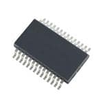
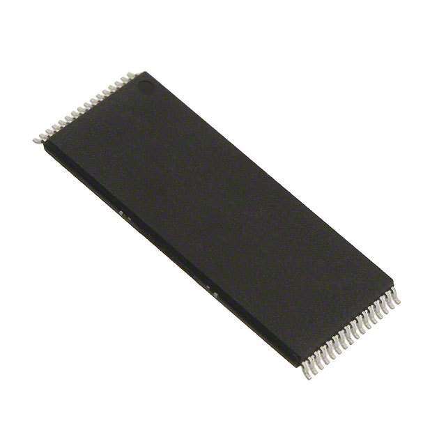
| 描述 | IC SRAM 256KBIT 45NS 28SOP静态随机存取存储器 256K 32K x 8 45ns 5v Async 静态随机存取存储器 5v |
| 产品分类 | |
| 品牌 | ISSI |
| 产品手册 | |
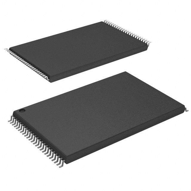
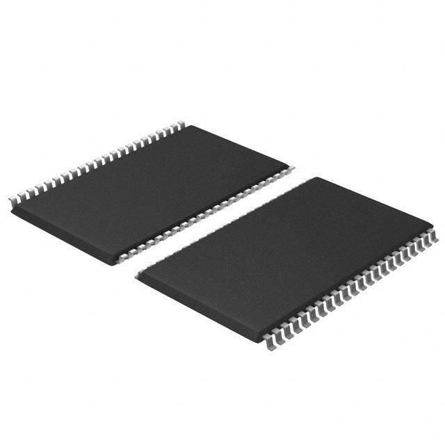
| 产品图片 |
|
| rohs | 符合RoHS无铅 / 符合限制有害物质指令(RoHS)规范要求 |
| 产品系列 | 内存,静态随机存取存储器,ISSI IS62C256AL-45ULI- |
| 数据手册 | |
| 产品型号 | IS62C256AL-45ULI |
| 产品种类 | 静态随机存取存储器 |
| 供应商器件封装 | 28-SOP |
| 其它名称 | 706-1043 |
| 包装 | 托盘 |
| 商标 | ISSI |
| 存储器类型 | SRAM - 异步 |
| 存储容量 | 256 kbit |
| 安装风格 | SMD/SMT |
| 封装 | Tube |
| 封装/外壳 | 28-SOIC(0.330",8.38mm 宽) |
| 封装/箱体 | SOP-28 |
| 工作温度 | -40°C ~ 85°C |
| 工厂包装数量 | 120 |
| 接口 | Parallel |
| 最大工作温度 | + 85 C |
| 最大工作电流 | 20 uA |
| 最大时钟频率 | 22 MHz |
| 最小工作温度 | - 40 C |
| 标准包装 | 120 |
| 格式-存储器 | RAM |
| 电压-电源 | 4.5 V ~ 5.5 V |
| 电源电压-最大 | 5.5 V |
| 电源电压-最小 | 4.5 V |
| 类型 | Asynchronous |
| 系列 | IS62C256AL |
| 组织 | 32 k x 8 |
| 访问时间 | 45 ns |
| 速度 | 45ns |


_renders/IS66WVE4M16EBLL-70BLI.jpg)


- 商务部:美国ITC正式对集成电路等产品启动337调查
- 曝三星4nm工艺存在良率问题 高通将骁龙8 Gen1或转产台积电
- 太阳诱电将投资9.5亿元在常州建新厂生产MLCC 预计2023年完工
- 英特尔发布欧洲新工厂建设计划 深化IDM 2.0 战略
- 台积电先进制程称霸业界 有大客户加持明年业绩稳了
- 达到5530亿美元!SIA预计今年全球半导体销售额将创下新高
- 英特尔拟将自动驾驶子公司Mobileye上市 估值或超500亿美元
- 三星加码芯片和SET,合并消费电子和移动部门,撤换高东真等 CEO
- 三星电子宣布重大人事变动 还合并消费电子和移动部门
- 海关总署:前11个月进口集成电路产品价值2.52万亿元 增长14.8%

_renders/IS61LPS102418B-200TQLI.jpg)
PDF Datasheet 数据手册内容提取
IS65C256AL IS62C256AL 32K x 8 LOW POWER CMOS STATIC RAM JULY 2015 FEATURES DESCRIPTION • Access time: 25 ns, 45 ns The ISSI IS62C256AL/IS65C256AL is a low power, 32,768 word by 8-bit CMOS static RAM. It is fabricated using • Low active power: 200 mW (typical) ISSI's high-performance, low power CMOS technology. • Low standby power — 150 µW (typical) CMOS standby When CE is HIGH (deselected), the device assumes a standby mode at which the power dissipation can be — 15 mW (typical) operating reduced down to 150 µW (typical) at CMOS input levels. • Fully static operation: no clock or refresh required Easy memory expansion is provided by using an active • TTL compatible inputs and outputs LOW Chip Select (CE) input and an active LOW Output Enable (OE) input. The active LOW Write Enable (WE) • Single 5V power supply controls both writing and reading of the memory. • Lead-free available • Industrial and Automotive temperatures available The IS62C256AL/IS65C256AL is pin compatible with other 32Kx8 SRAMs in plastic SOP or TSOP (Type I) package. FUNCTIONAL BLOCK DIAGRAM 32K X 8 A0-A14 DECODER MEMORY ARRAY VDD GND I/O I/O0-I/O7 DATA COLUMN I/O CIRCUIT CE CONTROL OE CIRCUIT WE Copyright © 2015 Integrated Silicon Solution, Inc. All rights reserved. ISSI reserves the right to make changes to this specification and its products at any time without notice. ISSI assumes no liability arising out of the application or use of any information, products or services described herein. Customers are advised to obtain the latest version of this device specification before relying on any published information and before placing orders for products. Integrated Silicon Solution, Inc. does not recommend the use of any of its products in life support applications where the failure or malfunction of the product can reasonably be expected to cause failure of the life support system or to significantly affect its safety or effectiveness. Products are not authorized for use in such applications unless Integrated Silicon Solution, Inc. receives written assurance to its satisfaction, that: a.) the risk of injury or damage has been minimized; b.) the user assume all such risks; and c.) potential liability of Integrated Silicon Solution, Inc is adequately protected under the circumstances Integrated Silicon Solution, Inc. — www.issi.com 1 Rev. E 07/20/2015
IS65C256AL IS62C256AL PIN CONFIGURATION PIN CONFIGURATION 28-Pin SOP 28-Pin TSOP A14 1 28 VDD OE 22 21 A10 A11 23 20 CE A12 2 27 WE A9 24 19 I/O7 A7 3 26 A13 A8 25 18 I/O6 A6 4 25 A8 A13 26 17 I/O5 A5 5 24 A9 WE 27 16 I/O4 A4 6 23 A11 VDD 28 15 I/O3 A14 1 14 GND A3 7 22 OE A12 2 13 I/O2 A2 8 21 A10 A7 3 12 I/O1 A1 9 20 CE A6 4 11 I/O0 A0 10 19 I/O7 A5 5 10 A0 A4 6 9 A1 I/O0 11 18 I/O6 A3 7 8 A2 I/O1 12 17 I/O5 I/O2 13 16 I/O4 GND 14 15 I/O3 PIN DESCRIPTIONS TRUTH TABLE A0-A14 Address Inputs Mode WE CE OE I/O Operation VDD Current CE Chip Select Input Not Selected X H X High-Z Isb1, Isb2 (Power-down) OE Output Enable Input Output Disabled H L H High-Z Icc1, Icc2 WE Write Enable Input Read H L L dout Icc1, Icc2 I/O0-I/O7 Input/Output Write L L X dIn Icc1, Icc2 Vdd Power GND Ground ABSOLUTE MAXIMUM RATINGS(1) Symbol Parameter Value Unit Vterm Terminal Voltage with Respect to GND –0.5 to +7.0 V tstg Storage Temperature –65 to +150 °C Pt Power Dissipation 0.5 W Iout DC Output Current (LOW) 20 mA Note: 1. Stress greater than those listed under ABSOLUTE MAXIMUM RATINGS may cause perma- nent damage to the device. This is a stress rating only and functional operation of the device at these or any other conditions above those indicated in the operational sections of this specification is not implied. Exposure to absolute maximum rating conditions for extended periods may affect reliability. 2 Integrated Silicon Solution, Inc. Rev. E 07/20/2015
IS65C256AL IS62C256AL OPERATING RANGE Part No. Range Ambient Temperature VDD IS62C256AL Commercial 0°C to +70°C 5V ± 10% IS62C256AL Industrial –40°C to +85°C 5V ± 10% IS65C256AL Automotive –40°C to +125°C 5V ± 10% DC ELECTRICAL CHARACTERISTICS Symbol Parameter Test Conditions Min. Max. Unit Voh Output HIGH Voltage Vdd = Min., Ioh = –1.0 mA 2.4 — V Vol Output LOW Voltage Vdd = Min., Iol = 2.1 mA — 0.4 V VIh Input HIGH Voltage 2.2 Vdd + 0.5 V VIl Input LOW Voltage(1) –0.3 0.8 V IlI Input Leakage GND ≤ VIn ≤ Vdd Com. –1 1 µA Ind. –2 2 Auto. –10 10 Ilo Output Leakage GND ≤ Vout ≤ Vdd, Com. –1 1 µA Outputs Disabled Ind. –2 2 Auto. –10 10 Note: 1. VIl = –3.0V for pulse width less than 10 ns. Integrated Silicon Solution, Inc. 3 Rev. E 07/20/2015
IS65C256AL IS62C256AL POWER SUPPLY CHARACTERISTICS(1) (Over Operating Range) -25 ns -45 ns Symbol Parameter Test Conditions Min. Max. Min. Max. Unit Icc1 Vdd Operating Vdd = Max., CE = VIl Com. — 15 — 15 mA Supply Current Iout = 0 mA, f = 0 Ind. — 20 — 20 Auto. — 25 — 25 Icc2 Vdd Dynamic Operating Vdd = Max., CE = VIl Com. — 25 — 20 mA Supply Current Iout = 0 mA, f = fmax Ind. — 30 — 25 Auto. — 35 — 30 typ. (2) 15 12 Isb1 TTL Standby Current Vdd = Max., Com. — 100 — 100 µA (TTL Inputs) VIn = VIh or VIl Ind. — 120 — 120 CE ≥ VIh, f = 0 Auto. — 150 — 150 Isb2 CMOS Standby Vdd = Max., Com. — 15 — 15 µA Current (CMOS Inputs) CE ≥ Vdd – 0.2V, Ind. — 20 — 20 VIn ≥ Vdd – 0.2V, or Auto. — 50 — 50 VIn ≤ 0.2V, f = 0 typ. (2) 5 5 Note: 1. At f = fmax, address and data inputs are cycling at the maximum frequency, f = 0 means no input lines change. 2. Typical values are measured at Vdd = 5.0V, Ta = 25oC and not 100% tested. CAPACITANCE(1,2) Symbol Parameter Conditions Max. Unit cIn Input Capacitance VIn = 0V 8 pF cout Output Capacitance Vout = 0V 10 pF Notes: 1. Tested initially and after any design or process changes that may affect these parameters. 2. Test conditions: Ta = 25°c, f = 1 MHz, Vdd = 5.0V. 4 Integrated Silicon Solution, Inc. Rev. E 07/20/2015
IS65C256AL IS62C256AL READ CYCLE SWITCHING CHARACTERISTICS(1) (Over Operating Range) -25 ns -45 ns Symbol Parameter Min. Max. Min. Max. Unit trc Read Cycle Time 25 — 45 — ns taa Address Access Time — 25 — 45 ns toha Output Hold Time 2 — 2 — ns tacs CE Access Time — 25 — 45 ns tdoe OE Access Time — 13 — 25 ns tlzoe(2) OE to Low-Z Output 0 — 0 — ns thzoe(2) OE to High-Z Output 0 12 0 20 ns tlzcs(2) CE to Low-Z Output 3 — 3 — ns thzcs(2) CE to High-Z Output 0 12 0 20 ns tPu(3) CE to Power-Up 0 — 0 — ns tPd(3) CE to Power-Down — 20 — 30 ns Notes: 1. Test conditions assume signal transition times of 5 ns or less, timing reference levels of 1.5V, input pulse levels of 0 to 3.0V and output loading specified in Figure 1. 2. Tested with the load in Figure 2. Transition is measured ±500 mV from steady-state voltage. Not 100% tested. 3. Not 100% tested. AC TEST CONDITIONS Parameter Unit Input Pulse Level 0V to 3.0V Input Rise and Fall Times 3 ns Input and Output Timing 1.5V and Reference Levels Output Load See Figures 1 and 2 AC TEST LOADS 1838 Ω 480 Ω 5V 5V OUTPUT OUTPUT 100 pF 993 Ω 5 pF 255 Ω Including Including jig and jig and scope scope Figure 1. Figure 2. Integrated Silicon Solution, Inc. 5 Rev. E 07/20/2015
IS65C256AL IS62C256AL AC WAVEFORMS READ CYCLE NO. 1(1,2) t RC ADDRESS t AA t t OHA OHA DOUT PREVIOUS DATA VALID DATA VALID READ1.eps READ CYCLE NO. 2(1,3) t RC ADDRESS t AA t OHA OE t DOE t HZOE CE t LZOE t ACS t t LZCS HZCS DOUT HIGH-Z DATA VALID CS_RD2.eps Notes: 1. WE is HIGH for a Read Cycle. 2. The device is continuously selected. OE, CE = VIl. 3. Address is valid prior to or coincident with CE LOW transitions. 6 Integrated Silicon Solution, Inc. Rev. E 07/20/2015
IS65C256AL IS62C256AL WRITE CYCLE SWITCHING CHARACTERISTICS(1,3) (Over Operating Range) -25 ns -45 ns Symbol Parameter Min. Max. Min. Max. Unit twc Write Cycle Time 25 — 45 — ns tscs CE to Write End 15 — 35 — ns taw Address Setup Time to Write End 15 — 25 — ns tha Address Hold from Write End 0 — 0 — ns tsa Address Setup Time 0 — 0 — ns tPwe(4) WE Pulse Width 15 — 25 — ns tsd Data Setup to Write End 12 — 20 — ns thd Data Hold from Write End 0 — 0 — ns thzwe(2) WE LOW to High-Z Output — 8 — 20 ns tlzwe(2) WE HIGH to Low-Z Output 0 — 0 — ns Notes: 1. Test conditions assume signal transition times of 5 ns or less, timing reference levels of 1.5V, input pulse levels of 0 to 3.0V and output loading specified in Figure 1. 2. Tested with the load in Figure 2. Transition is measured ±500 mV from steady-state voltage. Not 100% tested. 3. The internal write time is defined by the overlap of CE LOW and WE LOW. All signals must be in valid states to initiate a Write, but any one can go inactive to terminate the Write. The Data Input Setup and Hold timing are referenced to the rising or falling edge of the signal that terminates the write. 4. Tested with OE HIGH. AC WAVEFORMS WRITE CYCLE NO. 1 (CE Controlled, OE is HIGH or LOW) (1 ) t WC VALID ADDRESS ADDRESS t SA t SCS t HA CE t AW t PWE WE t t HZWE LZWE HIGH-Z DOUT DATA UNDEFINED t t SD HD DIN DATAIN VALID CS_WR1.eps Integrated Silicon Solution, Inc. 7 Rev. E 07/20/2015
IS65C256AL IS62C256AL AC WAVEFORMS WRITE CYCLE NO. 2 (OE is HIGH During Write Cycle) (1,2) t WC ADDRESS VALID ADDRESS t HA OE CE LOW t AW t PWE1 WE t SA t HZWE t LZWE HIGH-Z DOUT DATA UNDEFINED t t SD HD DIN DATAIN VALID CS_WR2.eps WRITE CYCLE NO. 3 (OE is LOW During Write Cycle) (1) t WC ADDRESS VALID ADDRESS t HA OE LOW CE LOW t AW t PWE2 WE t SA t HZWE t LZWE HIGH-Z DOUT DATA UNDEFINED t t SD HD DIN DATAIN VALID CS_WR3.eps Notes: 1. The internal write time is defined by the overlap of CE LOW and WE LOW. All signals must be in valid states to initiate a Write, but any one can go inactive to terminate the Write. The Data Input Setup and Hold timing are referenced to the rising or falling edge of the signal that terminates the write. 2. I/O will assume the High-Z state if OE = VIh. 8 Integrated Silicon Solution, Inc. Rev. E 07/20/2015
IS65C256AL IS62C256AL DATA RETENTION SWITCHING CHARACTERISTICS Symbol Parameter Test Condition Min. Typ. Max. Unit Vdr Vdd for Data Retention See Data Retention Waveform 2.0 5.5 V Idr Data Retention Current Vdd = 2.0V, CE ≥ Vdd – 0.2V Com. — — 15 µA VIn ≥ Vdd – 0.2V, or VIn ≤ Vss + 0.2V Ind. — — 20 Auto. — — 50 tsdr Data Retention Setup Time See Data Retention Waveform 0 — ns trdr Recovery Time See Data Retention Waveform trc — ns Note: 1. Typical Values are measured at Vdd = 5V, Ta = 25oC and not 100% tested. DATA RETENTION WAVEFORM (CE Controlled) tSDR Data Retention Mode tRDR VDD 4.5V 2.2V VDR CE1 ≥ VDD - 0.2V CE1 GND Integrated Silicon Solution, Inc. 9 Rev. E 07/20/2015
IS65C256AL IS62C256AL ORDERING INFORMATION Commercial Range: 0°C to +70°C Speed (ns) Order Part No. Package 45 IS62C256AL-45T TSOP IS62C256AL-45TL TSOP, Lead-free IS62C256AL-45UL Plastic SOP, Lead-free ORDERING INFORMATION Industrial Range: –40°C to +85°C Speed (ns) Order Part No. Package 25 IS62C256AL-25TI TSOP IS62C256AL-25ULI Plastic SOP, Lead-free 45 IS62C256AL-45TI TSOP IS62C256AL-45TLI TSOP, Lead-free IS62C256AL-45ULI Plastic SOP, Lead-free ORDERING INFORMATION Automotive Range: –40°C to +125°C Speed (ns) Order Part No. Package 25 IS65C256AL-25TA3 TSOP IS65C256AL-25TLA3 TSOP, Lead-free IS65C256AL-25ULA3 Plastic SOP, Lead-free 45 IS65C256AL-45TA3 TSOP IS65C256AL-45TLA3 TSOP, Lead-free IS65C256AL-45ULA3 Plastic SOP, Lead-free 10 Integrated Silicon Solution, Inc. Rev. E 07/20/2015
IS65C256AL IS62C256AL Integrated Silicon Solution, Inc. 11 Rev. E 07/20/2015
IS65C256AL IS62C256AL 12 Integrated Silicon Solution, Inc. Rev. E 07/20/2015
Mouser Electronics Authorized Distributor Click to View Pricing, Inventory, Delivery & Lifecycle Information: I SSI: IS62C256AL-45TLI IS62C256AL-45TLI-TR IS62C256AL-45ULI IS62C256AL-45ULI-TR IS65C256AL-25ULA3 IS65C256AL-25ULA3-TR IS65C256AL-25TLA3 IS65C256AL-25TLA3-TR IS62C256AL-25ULI IS62C256AL-25ULI-TR