ICGOO在线商城 > 集成电路(IC) > 线性 - 音頻放大器 > IS31AP4066D-QFLS2-TR
 Datasheet下载
- 型号: IS31AP4066D-QFLS2-TR
- 制造商: ISSI
- 库位|库存: xxxx|xxxx
- 要求:
| 数量阶梯 | 香港交货 | 国内含税 |
| +xxxx | $xxxx | ¥xxxx |
查看当月历史价格
查看今年历史价格
IS31AP4066D-QFLS2-TR产品简介:
ICGOO电子元器件商城为您提供IS31AP4066D-QFLS2-TR由ISSI设计生产,在icgoo商城现货销售,并且可以通过原厂、代理商等渠道进行代购。 IS31AP4066D-QFLS2-TR价格参考。ISSIIS31AP4066D-QFLS2-TR封装/规格:线性 - 音頻放大器, Amplifier IC 2-Channel (Stereo) Class AB 16-QFN (3x3)。您可以下载IS31AP4066D-QFLS2-TR参考资料、Datasheet数据手册功能说明书,资料中有IS31AP4066D-QFLS2-TR 详细功能的应用电路图电压和使用方法及教程。
| 参数 | 数值 |
| 产品目录 | 集成电路 (IC) |
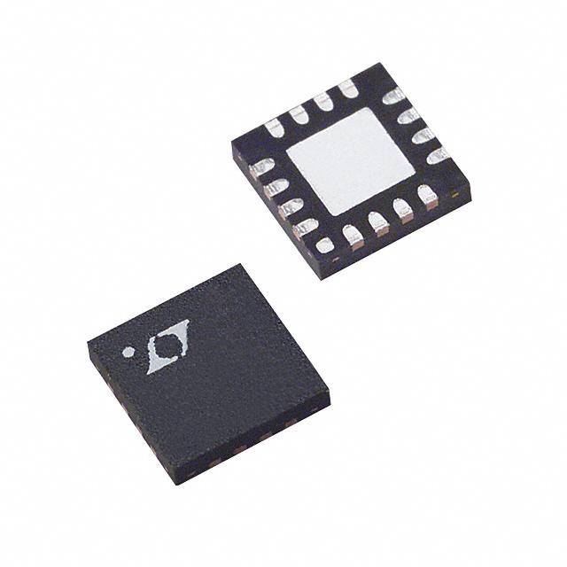
| 描述 | IC AUDIO AMP MONO 1.3W 16QFN |
| 产品分类 | |
| 品牌 | ISSI, Integrated Silicon Solution Inc |
| 数据手册 | |
| 产品图片 |
|
| 产品型号 | IS31AP4066D-QFLS2-TR |
| rohs | 无铅 / 符合限制有害物质指令(RoHS)规范要求 |
| 产品系列 | - |
| 不同负载时的最大输出功率x通道数 | 1.3W x 2 @ 8 欧姆 |
| 供应商器件封装 | 16-QFN(3x3) |
| 其它名称 | 706-1209-1 |
| 包装 | 剪切带 (CT) |
| 参考设计库 | http://www.digikey.com/rdl/4294959876/4294959895/1203 |
| 安装类型 | 表面贴装 |
| 封装/外壳 | 16-WFQFN 裸露焊盘 |
| 工作温度 | -40°C ~ 85°C (TA) |
| 标准包装 | 1 |
| 特性 | 消除爆音,热保护 |
| 电压-电源 | 2.7 V ~ 5.5 V |
| 类型 | AB 类 |
| 输出类型 | 2 通道(立体声) |


- 商务部:美国ITC正式对集成电路等产品启动337调查
- 曝三星4nm工艺存在良率问题 高通将骁龙8 Gen1或转产台积电
- 太阳诱电将投资9.5亿元在常州建新厂生产MLCC 预计2023年完工
- 英特尔发布欧洲新工厂建设计划 深化IDM 2.0 战略
- 台积电先进制程称霸业界 有大客户加持明年业绩稳了
- 达到5530亿美元!SIA预计今年全球半导体销售额将创下新高
- 英特尔拟将自动驾驶子公司Mobileye上市 估值或超500亿美元
- 三星加码芯片和SET,合并消费电子和移动部门,撤换高东真等 CEO
- 三星电子宣布重大人事变动 还合并消费电子和移动部门
- 海关总署:前11个月进口集成电路产品价值2.52万亿元 增长14.8%


PDF Datasheet 数据手册内容提取
IS31AP4066D DUAL 1.3W STEREO AUDIO AMPLIFIER January 2014 GENERAL DESCRIPTION KEY SPECIFICATIONS The IS31AP4066D is a dual bridge-connected audio P at R = 8Ω, V = 5V O L CC power amplifier which, when connected to a 5V supply, THD+N = 1% ---------------------- 1.3W (Typ.) will deliver 1.3W to an 8Ω load. THD+N = 10% --------------------- 1.6W (Typ.) The IS31AP4066D features a low-power consumption P at R = 8Ω, V = 4V O L CC shutdown mode and thermal shutdown protection. It THD+N = 1% ----------------------- 0.81W (Typ.) also utilizes circuitry to reduce “click-and-pop” during Shutdown current ------------------- 0.3μA (Typ.) device turn-on. Supply voltage range --------------- 2.7V ~ 5.5V QFN-16 (3mm × 3mm) package APPLICATIONS FEATURES Cell phones, PDA, MP4,PMP Portable and desktop computers Suppress “click-and-pop” Desktops audio system Thermal shutdown protection circuitry Multimedia monitors Micro power shutdown mode TYPICAL APPLICATION CIRCUIT Figure 1 Typical Application Circuit Integrated Silicon Solution, Inc. – www.issi.com 1 Rev. B, 01/03/2014
IS31AP4066D PIN CONFIGURATION Package Pin Configuration (Top View) D B D D N D N N G S G G 6 5 4 3 1 1 1 1 QFN-16 5 6 7 8 D D D S N N N S A G G G P Y B PIN DESCRIPTION No. Pin Description 1 OUTA+ Left channel positive output. 2,11 VCC Supply voltage. 3 OUTA- Left channel negative output. 4 INA Left channel input. 5~7,13,14,16 GND Ground. Bypass capacitor which provides the 8 BYPASS common mode voltage. 9 INB Right channel input. 10 OUTB- Right channel negative output. 12 OUTB+ Right channel positive output. Shutdown control, hold low for shutdown 15 SDB mode. Thermal Pad Connect to GND. Integrated Silicon Solution, Inc. – www.issi.com 2 Rev. B, 01/03/2014
IS31AP4066D ORDERING INFORMATION Industrial Range: -40°C to +85°C Order Part No. Package QTY/Reel IS31AP4066D-QFLS2-TR QFN-16, Lead-free 2500 Copyright © 2014 Integrated Silicon Solution, Inc. All rights reserved. ISSI reserves the right to make changes to this specification and its products at any time without notice. ISSI assumes no liability arising out of the application or use of any information, products or services described herein. Customers are advised to obtain the latest version of this device specification before relying on any published information and before placing orders for products. Integrated Silicon Solution, Inc. does not recommend the use of any of its products in life support applications where the failure or malfunction of the product can reasonably be expected to cause failure of the life support system or to significantly affect its safety or effectiveness. Products are not authorized for use in such applications unless Integrated Silicon Solution, Inc. receives written assurance to its satisfaction, that: a.) the risk of injury or damage has been minimized; b.) the user assume all such risks; and c.) potential liability of Integrated Silicon Solution, Inc is adequately protected under the circumstances Integrated Silicon Solution, Inc. – www.issi.com 3 Rev. B, 01/03/2014
IS31AP4066D ABSOLUTE MAXIMUM RATINGS Supply voltage, V -0.3V ~ +6.0V CC Voltage at any input pin -0.3V ~ V +0.3V CC Maximum junction temperature, T 150°C JMAX Storage temperature range, T -65°C ~ +150°C STG Operating temperature range, T −40°C ~ +85°C A ESD (HBM) 1kV ESD (CDM) 1kV Note: Stresses beyond those listed under “Absolute Maximum Ratings” may cause permanent damage to the device. These are stress ratings only and functional operation of the device at these or any other condition beyond those indicated in the operational sections of the specifications is not implied. Exposure to absolute maximum rating conditions for extended periods may affect device reliability. ELECTRICAL CHARACTERISTICS The following specifications apply for V = 5V, unless otherwise noted. CC Limits apply for T = 25°C. (Note 1 or specified) A Symbol Parameter Condition Min. Typ. Max. Unit V Supply voltage 2.7 5.5 V CC I Quiescent power supply current V = 0V, I = 0A 3.9 10.0 mA CC IN O I Shutdown current GND applied to the shutdown pin 0.3 2.5 μA SD V Shutdown input voltage high 1.4 V IH V Shutdown input voltage low 0.4 V IL t Turn on time C = 1μF (Note 2) 120 ms WU Bypass ELECTRICAL CHARACTERISTICS OPERATION The following specifications apply for V = 5V, unless otherwise noted. CC Limits apply for T = 25°C. (Note 2 or specified) A Symbol Parameter Condition Min. Typ. Max. Unit V Output offset voltage V = 0V 5.0 25.0 mV OS IN THD+N = 1%, f = 1kHz, R = 8Ω 1.3 W L Po Output power THD+N = 10%, f = 1kHz, R = 8Ω 1.6 W L Total harmonic THD+N f = 1kHz, A = 2, R = 8Ω, P = 1W 0.1 % distortion +noise V L O Input floating, 217Hz, V = 200mV Ripple p-p 80.0 dB C = 1μF, R = 8Ω Bypass L Input floating 1kHz, V = 200mV Ripple p-p 70.0 dB Power supply rejection CBypass = 1μF, RL = 8Ω PSRR ratio Input GND 217Hz, V = 200mV Ripple p-p 60.0 dB C = 1μF, R =8Ω Bypass L Input GND 1kHz V = 200mV Ripple p-p 60.0 dB C = 1μF, R = 8Ω Bypass L X Channel separation f = 1kHz, C = 1μF -100 dB Talk Bypass V Output noise voltage 1kHz, A-weighted 7.0 μV NO Integrated Silicon Solution, Inc. – www.issi.com 4 Rev. B, 01/03/2014
IS31AP4066D ELECTRICAL CHARACTERISTICS The following specifications apply for V = 3V, unless otherwise noted. CC Limits apply for T = 25°C. (Note 1 or specified) A Symbol Parameter Condition Min. Typ. Max. Unit I Quiescent power supply current V = 0V, I = 0A 2.6 6.5 mA CC IN O I Shutdown current GND applied to the shutdown pin 0.1 2.2 μA SD V Shutdown input voltage high 1.1 V IH V Shutdown input voltage low 0.4 V IL t Turn on time C = 1μF (Note 2) 110 ms WU Bypass ELECTRICAL CHARACTERISTICS OPERATION The following specifications apply for V = 3V, unless otherwise noted. CC Limits apply for T = 25°C. (Note 2 or specified) A Symbol Parameter Condition Min. Typ. Max. Unit V Output offset voltage V = 0V 2.5 25.0 mV OS IN THD+N = 1%, f = 1kHz, R = 8Ω 0.5 W L Po Output power THD+N = 10%, f = 1kHz, R = 8Ω 0.6 W L Total harmonic THD+N f = 1kHz, A = 2, R = 8Ω, P = 0.3W 0.1 % distortion+noise V L O Input floating, 217Hz, V = 200mV Ripple p-p 75.0 dB C = 1μF, R = 8Ω Bypass L Input floating 1kHz, V = 200mV Ripple p-p 70.0 dB Power supply CBypass = 1μF, RL = 8Ω PSRR rejection ratio Input GND 217Hz, V = 200mV Ripple p-p 62.0 dB C = 1μF, R =8Ω Bypass L Input GND 1kHz V = 200mV Ripple p-p 62.0 dB C = 1μF, R = 8Ω Bypass L X Channel separation f = 1kHz, C = 1μF -100 dB Talk Bypass V Output noise voltage 1kHz, A-weighted 7.0 uV NO Note1: All parameters are production tested at 25°C, functional operation of the device and parameters specified over other temperature range, are guaranteed by design, characterization and process control. Note 2: Guaranteed by design. Integrated Silicon Solution, Inc. – www.issi.com 5 Rev. B, 01/03/2014
IS31AP4066D TYPICAL PERFORMANCE CHARACTERISTICS Vcc = 5V Vcc = 3V RL RL f = 1kHz f = 1kHz Figure 2 THD+N vs. Output Power Figure 3 THD+N vs. Output Power Vcc = 5V Vcc = 3V R R L L Po = 1W Po=300mW Figure 4 THD+N vs. Frequency Figure 5 THD+N vs. Frequency Vcc = 5V Vcc = 3V R R L L Input GND Input GND Figure 6 PSRR vs. Frequency Figure 7 PSRR vs. Frequency Integrated Silicon Solution, Inc. – www.issi.com 6 Rev. B, 01/03/2014
IS31AP4066D Vcc = 5V Vcc = 5V RL RL Input Floating Figure 8 PSRR vs. Frequency Figure 9 Crosstalk vs. Frequency Vcc = 3V Vcc= 5V R L R L Input Floating A-Weighting Figure 10 PSRR vs. Frequency Figure 11 Noise Floor Vcc = 5V Vcc= 3V RL RL Figure 12 Frequency Response Figure 13 Frequency Response Integrated Silicon Solution, Inc. – www.issi.com 7 Rev. B, 01/03/2014
IS31AP4066D Vcc = 3V Vcc= 3V R R L L A-Weighting Figure 14 Crosstalk vs. Frequency Figure 15 Noise Floor R L Top Side Bottom Side Vcc = 5V R L f = 1kHz Output Power (W) Figure 16 Dropout Voltage vs. Supply Voltage Figure 17 Power Dissipation vs. Output Power R L f = 1kHz THD+N = 10% THD+N = 1% Figure18 Output Power vs. Supply Voltage Integrated Silicon Solution, Inc. – www.issi.com 8 Rev. B, 01/03/2014
IS31AP4066D FUNCTIONAL BLOCK DIAGRAM VCC INA OUTA- OUTA+ BYPASS SDB OUTB+ OUTB- INB GND Integrated Silicon Solution, Inc. – www.issi.com 9 Rev. B, 01/03/2014
IS31AP4066D APPLICATION INFORMATION EXPOSED-DAP PACKAGE PCB MOUNTING POWER SUPPLY BYPASSING CONSIDERATIONS As with any power amplifier, proper supply bypassing The IS31AP4066D’s QFN (die attach paddle) package is critical for low noise performance and high power provides a low thermal resistance between the die and supply rejection. Applications that employ a 5V the PCB to which the part is mounted and soldered. regulator typically use a 10μF in parallel with a 0.1μF This allows rapid heat transfer from the die to the filter capacitor to stabilize the regulator’s output, surrounding PCB copper traces, ground plane and, reduce noise on the supply line, and improve the finally, surrounding air. supply’s transient response. However, their presence does not eliminate the need for a local 1.0μF tantalum The QFN package must have it’s DAP soldered to a bypass capacitance connected between the copper pad on the PCB. The DAP’s PCB copper pad is IS31AP4066D’s supply pins and ground. Keep the connected to a large plane of continuous unbroken length of leads and traces that connect capacitors copper. This plane forms a thermal mass and heat sink between the IS31AP4066D’s power supply pin and and radiation area. Place the heat sink area on either ground as short as possible. outside plane in the case of a two-sided PCB, or on an inner layer of a board with more than two layers. MICRO-POWER SHUTDOWN BRIDGE CONFIGURATION EXPLANATION The voltage applied to the SDB pin controls the IS31AP4066D’s shutdown function. Activate As shown in Figure 1, the IS31AP4066D consists of micro-power shutdown by applying GND to the SDB two pairs of operational amplifiers, forming a pin. When active, the IS31AP4066D’s micro-power two-channel (Channel A and Channel B) stereo shutdown feature turns off the amplifier’s bias circuitry, amplifier. External feedback resistors R and input F reducing the supply current. The low 0.3μA typical resistors R set the closed-loop gain of Amp A (OUT-) IN shutdown current is achieved by applying a voltage and Amp B OUT-) whereas two internal 20kΩ resistors that is as near as GND as possible to the SDB pin. set Amp A’s (OUT+) and Amp B’s (OUT+) gain at 1. The IS31AP4066D drives a load, such speaker, There are a few ways to control the micro-power connected between the two amplifier outputs, OUTA− shutdown. These include using a single-pole, and OUTA+. single-throw switch, a microprocessor, or a microcontroller. When use a switch, connect an Figure 1 shows that Amp A’s (OUT-) output serves as external 100kΩ resistor between the SDB pin and Amp A’s (OUT+) input. This results in both amplifiers GND. Select normal amplifier operation by closing the producing signals identical in magnitude, but 180° out switch. Opening the switch sets the SDB pin to ground of phase. Taking advantage of this phase difference, a through the 100kΩ resistor, which activates the load is placed between OUTA− and OUTA+ and driven micropower shutdown. The switch and resistor differentially (commonly referred to as “bridge mode”). guarantee that the SDB pin will not float. This prevents This results in a differential gain of unwanted state changes. In a system with a A = 2×(R /R ) (1) microprocessor or a microcontroller, use a digital V F IN output to apply the control voltage to the SDB pin. Bridge mode amplifiers are different from single-ended Driving the SDB pin with active circuitry eliminates the amplifiers that drive loads connected between a single pull up resistor. amplifier’s output and ground. For a given supply voltage, bridge mode has a distinct advantage over the SELECTING PROPER EXTERNAL COMPONENTS single-ended configuration: its differential output Optimizing the IS31AP4066D’s performance requires doubles the voltage swing across the load. This properly selecting external components. Though the produces four times the output power when compared IS31AP4066D operates well when using external to a single-ended amplifier under the same conditions. components with wide tolerances, best performance is This increase in attainable output power assumes that achieved by optimizing component values. the amplifier is not current limited The IS31AP4066D is unity-gain stable, giving a Another advantage of the differential bridge output is designer maximum design flexibility. The gain should no net DC voltage across the load. This is be set to no more than a given application requires. accomplished by biasing Channel A’s and Channel B’s This allows the amplifier to achieve minimum THD+N outputs at half-supply. This eliminates the coupling and maximum signal-to-noise ratio. These parameters capacitor that single supply, single ended amplifiers are compromised as the closed-loop gain increases. require. Eliminating an output coupling capacitor in a However, low gain demands input signals with greater single-ended configuration forces a single-supply voltage swings to achieve maximum output power. amplifier’s half-supply bias voltage across the load. Fortunately, many signal sources such as audio This increases internal IC power dissipation and may CODECs have outputs of 1VRMS (2.83V ). Please permanently damage loads such as speakers. P-P Integrated Silicon Solution, Inc. – www.issi.com 10 Rev. B, 01/03/2014
IS31AP4066D refer to the Audio Power Amplifier Design section for Choosing C equal to 1.0μF along with a small BYPASS more information on selecting the proper gain. value of C (in the range of 0.1μF to 0.39μF), IN produces a click-less and pop-less shutdown function. INPUT CAPACITOR VALUE SELECTION As discussed above, choosing C no larger than IN Amplifying the lowest audio frequencies requires high necessary for the desired band with helps minimize value input coupling capacitors C in Figure 1. A high click-and-pop. Connecting a 1μF capacitor, C , IN BYPASS value capacitor can be expensive and may between the BYPASS pin and ground improves the compromise space efficiency in portable designs. In internal bias voltage’s stability and improves the many cases, however, the speakers used in portable amplifier’s PSRR. systems, whether internal or external, have little ability OPTIMIZING CLICK-AND-POP REDUCTION to reproduce signals below 150Hz. Applications using PERFORMANCE speakers with this limited frequency response reap little improvement by using large input capacitor. The IS31AP4066D contains circuitry that minimizes turn-on and shutdown transients or “click-and-pop”. Besides effecting system cost and size, C have an IN For this discussion, turn-on refers to either applying effect on the IS31AP4066D’s click and pop the power supply voltage or when the shutdown mode performance. When the supply voltage is first applied, is deactivated. When the part is turned on, an internal a transient (pop) is created as the charge on the input current source changes the voltage of the BYPASS pin capacitor changes from zero to a quiescent state. The in a controlled, linear manner. Ideally, the input and magnitude of the pop is directly proportional to the outputs track the voltage applied to the BYPASS pin. input capacitor’s size. Higher value capacitors need The gain of the internal amplifiers remains unity until more time to reach a quiescent DC voltage (usually the voltage on the bypass pin reaches 1/2V . As soon V /2) when charged with a fixed current. The CC CC as the voltage on the bypass pin is stable, the device amplifier’s output charges the input capacitor through becomes fully operational. Although the BYPASS pin the feedback resistors, R . Thus, pops can be F current cannot be modified, changing the size of minimized by selecting an input capacitor value that is C alters the device’s turn-on time and the no higher than necessary to meet the desired −3dB BYPASS magnitude of “click-and-pop”. Increasing the value of frequency. C reduces the magnitude of turn-on pops. BYPASS A shown in Figure 1, the input resistors R and the However, this presents a tradeoff: as the size of IN input capacitors C produce a −3dB high pass filter C increases, the turn-on time increases. There is IN BYPASS cutoff frequency that is found using Equation (2). a linear relationship between the size of C and BYPASS the turn-on time. Here are some typical turn-on times f = 1/2πR C (2) -3dB IN IN for various values of C (all tested at V = 5V): BYPASS CC As an example when using a speaker with a low frequency limit of 150Hz, C , using Equation (2) is C t INA BYPASS ON 0.053μF. The 0.33μF C allows the IS31AP4066D to INA 0.01μF 13ms drive high efficiency, full range speaker whose response extends below 30Hz. 0.1μF 26ms BYPASS CAPACITOR VALUE SELECTION 0.22μF 44ms Besides minimizing the input capacitor size, careful 0.47μF 68ms consideration should be paid to value of C , the BYPASS 1.0μF 120 ms capacitor connected to the BYPASS pin. Since C BYPASS determines how fast the IS31AP4066D settles to In order eliminate “click-and-pop”; all capacitors must quiescent operation, its value is critical when be discharged before turn-on. Rapidly switching VCC minimizing turn-on pops. The slower the on and off may not allow the capacitors to fully IS31AP4066D’s outputs ramp to their quiescent DC discharge, which may cause “click-and-pop”. voltage (nominally 1/2V ), the smaller the turn-on pop. CC Integrated Silicon Solution, Inc. – www.issi.com 11 Rev. B, 01/03/2014
IS31AP4066D CLASSIFICATION REFLOW PROFILES Profile Feature Pb-Free Assembly Preheat & Soak 150°C Temperature min (Tsmin) 200°C Temperature max (Tsmax) 60-120 seconds Time (Tsmin to Tsmax) (ts) Average ramp-up rate (Tsmax to Tp) 3°C/second max. Liquidous temperature (TL) 217°C Time at liquidous (tL) 60-150 seconds Peak package body temperature (Tp)* Max 260°C Time (tp)** within 5°C of the specified Max 30 seconds classification temperature (Tc) Average ramp-down rate (Tp to Tsmax) 6°C/second max. Time 25°C to peak temperature 8 minutes max. Figure 19 Classification Profile Integrated Silicon Solution, Inc. – www.issi.com 12 Rev. B, 01/03/2014
IS31AP4066D PACKAGE INFORMATION QFN-16 Note: All dimensions in millimeters unless otherwise stated. Integrated Silicon Solution, Inc. – www.issi.com 13 Rev. B, 01/03/2014