ICGOO在线商城 > IRS2500SPBF
- 型号: IRS2500SPBF
- 制造商: International Rectifier
- 库位|库存: xxxx|xxxx
- 要求:
| 数量阶梯 | 香港交货 | 国内含税 |
| +xxxx | $xxxx | ¥xxxx |
查看当月历史价格
查看今年历史价格
IRS2500SPBF产品简介:
ICGOO电子元器件商城为您提供IRS2500SPBF由International Rectifier设计生产,在icgoo商城现货销售,并且可以通过原厂、代理商等渠道进行代购。 提供IRS2500SPBF价格参考¥询价-¥询价以及International RectifierIRS2500SPBF封装/规格参数等产品信息。 你可以下载IRS2500SPBF参考资料、Datasheet数据手册功能说明书, 资料中有IRS2500SPBF详细功能的应用电路图电压和使用方法及教程。
| 参数 | 数值 |
| 产品目录 | 集成电路 (IC)半导体 |
| 描述 | IC PFC功率因数校正 - PFC PFC controller IC |
| 产品分类 | |
| 品牌 | International Rectifier |
| 产品手册 | |
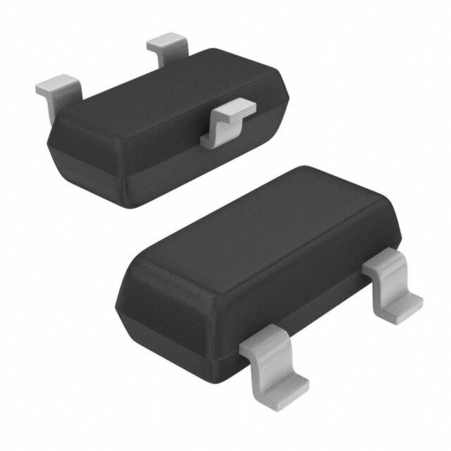
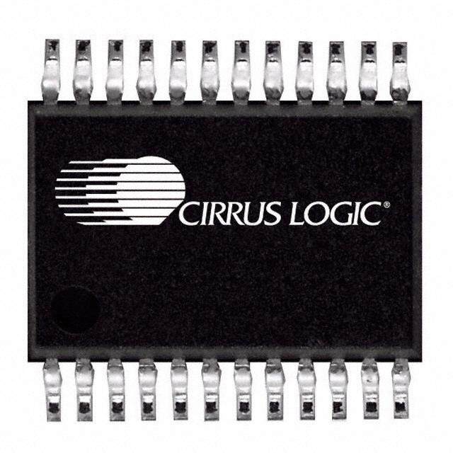
| 产品图片 |
|
| rohs | 符合RoHS无铅 / 符合限制有害物质指令(RoHS)规范要求 |
| 产品系列 | 电源管理 IC,功率因数校正 - PFC,International Rectifier IRS2500SPBF* |
| 数据手册 | |
| 产品型号 | IRS2500SPBF |
| 产品培训模块 | http://www.digikey.cn/PTM/IndividualPTM.page?site=cn&lang=zhs&ptm=25857http://www.digikey.cn/PTM/IndividualPTM.page?site=cn&lang=zhs&ptm=26250 |
| 产品种类 | 功率因数校正 - PFC |
| 商标 | International Rectifier |
| 安装风格 | SMD/SMT |
| 封装 | Tube |
| 封装/箱体 | SOIC-8 |
| 工厂包装数量 | 95 |
| 最大功率耗散 | 0.625 W |
| 标准包装 | 95 |
| 特色产品 | http://www.digikey.cn/product-highlights/cn/zh/international-rectifier-irs2500-upfc-ic/2325 |
| 配用 | /product-detail/zh/IRPLPFC1/IRPLPFC1-ND/4815113 |






- 商务部:美国ITC正式对集成电路等产品启动337调查
- 曝三星4nm工艺存在良率问题 高通将骁龙8 Gen1或转产台积电
- 太阳诱电将投资9.5亿元在常州建新厂生产MLCC 预计2023年完工
- 英特尔发布欧洲新工厂建设计划 深化IDM 2.0 战略
- 台积电先进制程称霸业界 有大客户加持明年业绩稳了
- 达到5530亿美元!SIA预计今年全球半导体销售额将创下新高
- 英特尔拟将自动驾驶子公司Mobileye上市 估值或超500亿美元
- 三星加码芯片和SET,合并消费电子和移动部门,撤换高东真等 CEO
- 三星电子宣布重大人事变动 还合并消费电子和移动部门
- 海关总署:前11个月进口集成电路产品价值2.52万亿元 增长14.8%


PDF Datasheet 数据手册内容提取
IRS2500SPBF TRANSITION MODE PFC CONTROL IC Product Summary Features Boost PFC Control IC Topology Boost Wide input range for universal AC line input I & I (typical) 500 mA / 500 mA Low THD o+ o- Voltage mode control tr & tf (typical) 60 ns / 30 ns Critical-conduction / transition mode operation Static and dynamic DC output over-voltage protection Burst mode operation at very light load Cycle by cycle over-current protection Micro-power startup (<50A) Low quiescent current Latch immunity and ESD protection Package Noise immunity Typical Applications Power supplies Lighting ballasts and drivers 8-Lead SOIC IRS2500SPBF Ordering Information Standard Pack Base Part Number Package Type Complete Part Number Form Quantity Tube/Bulk 95 IRS2500SPBF IRS2500SPBF SO8N Tape and Reel 2500 IRS2500STRPBF 1 www.irf.com © 2015 International Rectifier Submit Datasheet Feedback September 6, 2015
IRS2500SPBF Table of Contents Page Description 3 Qualification Information 4 Absolute Maximum Ratings 5 Recommended Operating Conditions 5 Electrical Characteristics 6 Functional Block Diagram 8 Input / Output Pin Equivalent Circuit Diagram 8 Lead Definitions 9 Lead Assignments 9 Application Information and Additional Details 10 PCB Layout Guidelines 13 PFC Design Equations (for Boost converter) 14 Operating Characteristics over Temperature 15 Package Details 17 Tape and Reel Details 18 Part Marking Information 19 2 www.irf.com © 2015 International Rectifier Submit Datasheet Feedback September 6, 2015
IRS2500SPBF Description The IRS2500 is a fully integrated, fully protected power factor correcting SMPS control IC designed to drive Boost switching regulators providing high power factor. Typical applications are PFC pre-regulators for SMPS and electronic ballasts for fluorescent, HID or LED lighting. The IRS2500 is pin compatible with most industry standard critical conduction mode PFC control ICs, with additional improvements to increase performance. The IRS2500 based converter provides high PF, low THD and stable DC bus regulation over a wide line/load range. Protection features include cycle by cycle over-current protection and output over voltage protection. Typical Connection Diagram D BUS + Rectified AC Line + Regulated DC Bus R R VBUS1 S D VCC CVBUS RVBUS VBUS VCC 1 8 RIN CCOMP COMP2 00 7OUT CVCC CBUS+ RDC VDC 25 COM 3 6 S OC R ZX 4 5 I RZX R GPFC MPFC R OC1 ROC COC - Rectified AC Line - Regulated DC Bus 3 www.irf.com © 2015 International Rectifier Submit Datasheet Feedback September 6, 2015
IRS2500SPBF † Qualification Information Industrial†† Comments: This family of ICs has passed JEDEC’s Industrial Qualification Level qualification. IR’s Consumer qualification level is granted by extension of the higher Industrial level. MSL2††† 260°C Moisture Sensitivity Level SOIC8 (per IPC/JEDEC J-STD-020) Class B Machine Model (per JEDEC standard JESD22-A115) ESD Class 2 Human Body Model (per EIA/JEDEC standard EIA/JESD22-A114) Class I, Level A IC Latch-Up Test (per JESD78) RoHS Compliant Yes † Qualification standards can be found at International Rectifier’s web site http://www.irf.com/ †† Higher qualification ratings may be available should the user have such requirements. Please contact your International Rectifier sales representative for further information. ††† Higher MSL ratings may be available for the specific package types listed here. Please contact your International Rectifier sales representative for further information. 4 www.irf.com © 2015 International Rectifier Submit Datasheet Feedback September 6, 2015
IRS2500SPBF Absolute Maximum Ratings Absolute maximum ratings indicate sustained limits beyond which damage to the device may occur. All voltage parameters are absolute voltages referenced to COM. All currents are defined positive into any lead. The thermal resistance and power dissipation ratings are measured under board mounted and still air conditions. Symbol Definition Min. Max. Units VCC Supply Voltage† -0.3 VCLAMP VOUT Gate Driver Output Voltage -0.3 VCC + 0.3 V Maximum allowable output current (OUT) due to external IOMAX -500 500 mA power transistor miller effect ICC VCC current 0 25 mA VCOMP COMP Pin Voltage -0.3 VCC + 0.3 VOC OC Pin Voltage VVBUS VBUS Pin Voltage V VDC VDC Pin Voltage -0.3 7.0 VZX ZX Pin Voltage ICOMP COMP Pin Current IZX ZX Pin Current -5 5 mA IOC OC Pin Current PD Package Power Dissipation @ TA +25ºC --- 0.625 W RJA Thermal Resistance, Junction to Ambient --- 128 ºC/W TJ Junction Temperature -55 150 TS Storage Temperature -55 150 ºC TL Lead Temperature (soldering, 10 seconds) --- 300 † This IC contains a zener clamp structure between the chip V and COM which has a nominal breakdown voltage of CC 20V. This supply pin should not be driven by a DC, low impedance power source greater than the V specified in CLAMP the Electrical Characteristics section. Recommended Operating Conditions For proper operation the device should be used within recommended conditions. Symbol Definition Min. Max. Units VCC Supply Voltage† VCCUV+ VCLAMP V ICC VCC Supply Current 0 10 IOC OC Pin Current mA -1 1 IZX ZX Pin Current TJ Junction Temperature -25 125 ºC 5 www.irf.com © 2015 International Rectifier Submit Datasheet Feedback September 6, 2015
IRS2500SPBF Electrical Characteristics V = 14 V +/- 0.25 V, C =1000pF, C =0.1μF, T =25 °C unless otherwise specified. CC OUT VCC A Symbol Definition Min Typ Max Units Test Conditions Supply Characteristics VCC Supply Undervoltage Positive Going VCCUV+ 11.5 12.5 13.5 Threshold VCC Supply Undervoltage Negative Going VCCUV- 9.5 10.5 11.5 Threshold VCC Supply Undervoltage Lockout VUVHYS 1.5 2.0 3.0 Hysteresis IQCCUV UVLO Mode VCC Quiescent Current --- 30 50 µA VCC = 8V VBUS=2.5V PFC off time = ICC VCC Supply Current --- 2.3 5.0 mA 5us VCLAMP VCC Zener Clamp Voltage --- 20.0 --- V ICC = 10mA Error Amplifier Characteristics ICOMP COMP Pin Error Amplifier Output Current VVBUS = 2.4V --- 10 --- SOURCE Sourcing VCOMP=4.0V mA ICOMP COMP Pin Error Amplifier Output Current VVBUS = 2.6V --- -23 --- SINK Sinking VCOMP=4.0V Error Amplifier Output Voltage Swing (high VBUS=2.0V VCOMPOH --- 6.0 --- state) ICOMP=-0.5mA Error Amplifier Output Voltage Swing (low VBUS=3.0V VCOMPOL --- 0.25 --- V state) ICOMP=+0.5mA Error Amplifier Output Voltage in Fault VCOMPFLT --- 0 --- VBUS=3.0V Mode IVBUS Input bias current --- --- -1 µA VBUS=0 to 3V Gv Voltage gain 60 80 --- dB Open loop GB Bandwidth --- 1 --- MHz Control Characteristics VVBUS VBUS Internal Reference Voltage 2.46 2.5 2.54 VZX+ ZX Pin Threshold Voltage (Arm) --- 1.6 --- VCOMP = 4.0V VZX- ZX Pin Threshold Voltage (Trigger) --- 0.7 --- V VZXclamp ZX pin Clamp Voltage (high state) --- 5.2 --- IZX = 1mA VDCclamp VDC pin Clamp Voltage --- 5.2 --- IDC = 1mA VBUS=2.5V tBLANK OC pin current-sensing blank time --- 320 --- ns VCOMP=4.0V ZX = 0,VCOMP = tWD PFC Watch-dog Pulse Interval --- 400 --- µs 4.0V ZX = 0,VCOMP = tONMIN PFC Minimum ON time --- 0.3 --- µs 0.25V ZX = 0,VCOMP = tONMAX PFC Maximum ON Time 10 50 --- µs 6.0V, VDC = 2V 6 www.irf.com © 2015 International Rectifier Submit Datasheet Feedback September 6, 2015
IRS2500SPBF Electrical Characteristics (cont’d) VCC = 14V +/- 0.25V, COUT = 1000pF, VCOMP = VOC = VBUS = VZX = 0V, TA=25C unless otherwise specified. Protection Circuitry Characteristics VOCTH OC Pin Over-current Sense Threshold 0.93 1.1 1.22 V VBUS Over-voltage Comparator Guaranteed by VVBUSOV 2.7 Threshold design VVBUSOV VBUS Over-voltage Comparator Guaranteed by 50 100 150 mV HYS Hysteresis design Dynamic Over-voltage detection ICOMPOV+ 30 threshold µA ICOMPOV- Dynamic Over-voltage detection reset 8 Gate Driver Output Characteristics VOL Low-Level Output Voltage --- 0 100 mV IO = 0 VOH High-Level Output Voltage --- 0 11 V IO = 0 tr Turn-On Rise Time --- 60 110 ns tf Turn-Off Fall Time --- 30 70 I0+ Source Current --- 500 --- mA I0- Sink Current --- 500 --- 7 www.irf.com © 2015 International Rectifier Submit Datasheet Feedback September 6, 2015
IRS2500SPBF Functional Block Diagram VCC COM OC 4 LEADING EDGE 8 6 VOCTH BLANKING UVLO VCLAMP VBUS 1 OVP ENN VVBUS VCC VVBUSOV 7 OUT COMP 2 S Q R Q VDC 3 ON TIME MODULATOR VDCCLAMP WATCHDOG S Q TIMER R1 R2 Q VCOMPOL ZX 5 VZX VZXCLAMP Input / Output Pin Equivalent Circuit Diagrams VCC VBUS, ESD VDC, Diode COMP, OC, ZX, VCLAMP OUT ESD Diode COM 8 www.irf.com © 2015 International Rectifier Submit Datasheet Feedback September 6, 2015
IRS2500SPBF Lead Definitions Symbol Description VBUS DC Bus Sensing Input COMP PFC Error Amplifier Compensation VDC Full Wave Voltage Input OC PFC Current Sensing Input ZX PFC Zero-Crossing Detection COM IC Power & Signal Ground OUT Gate Drive Output VCC Logic & Low-Side Gate Driver Supply Lead Assignments Pin # Symbol Description VBUS VCC 1 8 1 VBUS DC Bus Sensing Input 0 COMP 2 0 7 OUT 2 COMP PFC Error Amplifier Compensation 5 3 VDC Full Wave Voltage Input 2 4 OC PFC Current Sensing Input VDC COM 3 S 6 5 ZX PFC Zero-Crossing Detection R I ZX 6 COM IC Power & Signal Ground OC 4 5 7 OUT Gate Drive Output 8 VCC Logic & Low-Side Gate Driver Supply 9 www.irf.com © 2015 International Rectifier Submit Datasheet Feedback September 6, 2015
IRS2500SPBF IRS2500SPBF Application Information and Additional Details When the switch MPFC is turned on, the inductor LPFC is connected between the rectified line input Power factor correction is required for many (+) and (-) causing the current in LPFC to increase electrical appliances in order to minimize reactive linearly. When MPFC is turned off, LPFC is current losses in AC power transmission lines. The connected between the rectified line input (+) and degree to which an electronic system matches an the DC bus capacitor CBUS through diode DPFC. ideal purely resistive load; is measured by the The stored energy in LPFC is transferred to the phase shift (displacement) between the input output supplying current into CBUS. MPFC is voltage and current and the amount of current turned on and off at a high frequency and the waveform distortion. This can also be considered as voltage on CBUS rises to a determined level. The how well the shape of the input current waveform voltage feedback loop of the IRS2500 regulates the matches the shape of the sinusoidal input voltage. output to the desired level by continuously The power factor (PF) is defined as the ratio monitoring the DC output and adjusting the on-time between real power and apparent power with a of MPFC accordingly. If the output voltage is too maximum value of 1.0 representing a totally high, the on-time is decreased and if it is too low, resistive load where the current waveform shape the on-time is increased. This negative feedback matches the voltage waveform shape exactly. The control loop operates with a slow loop speed and a distortion of the input current waveform is quantified low loop gain such that the average inductor current by the total harmonic distortion (THD), which is the smoothly follows the low-frequency line input sum of all individual harmonics present the voltage to obtain high power factor and low THD. waveform expressed as a percentage. The loop speed must be slow with respect to the An ideal power factor of 1.0 corresponds to zero AC line frequency so that there is no appreciable phase-shift and 0% THD. This represents a purely change in the on time during a single line half cycle. sinusoidal input current waveform perfectly in phase This allows the current to follow shape of the with a purely sinusoidal line voltage. The lower the sinusoidal voltage. power factor the more current is needed to supply the same power to the load resulting is higher V, I transmission line conduction losses. High PF and low THD therefore provide optimum efficiency. The IRS2500 forms the basis of an active power factor correction (PFC) pre-converter to convert AC line input to a regulated DC bus. The control method implemented in the IRS2500 is typically used in a Boost converter (Figure 8). The IRS2500 operates in critical-conduction mode t (CrCM), also known as transition or boundary Figure 9: Sinusoidal line input voltage (solid line), mode. This means that during each switching cycle triangular PFC Inductor current and smoothed of the PFC MOSFET, the inductor current sinusoidal line input current (dashed line) over one discharges to zero before turning the PFC MOSFET half-cycle of the AC line input voltage. on again. The PFC MOSFET is turned on and off at a much higher frequency (>10kHz) than the line Corrections to the output voltage therefore require input frequency (50 to 60Hz). several line cycles. During the AC line half cycle the on-time remains effectively constant while the off- time varies. This is determined by the inductor LPFC DPFC current discharging to zero resulting in a system DC Bus (+) where the switching frequency is free-running and constantly changing from a high frequency near the + zero crossing of the AC input line voltage, to a lower frequency at the peaks (Figure 9). CBUS MPFC When the line instantaneous input voltage is low (near the zero crossing), the inductor current will (-) increase only a small amount and the discharge Figure 8: Boost converter circuit. time will be short resulting in a high switching 10 www.irf.com © 2015 International Rectifier Submit Datasheet Feedback September 6, 2015
IRS2500SPBF IRS2500SPBF frequency. When this voltage is high (near the peak), the inductor current will charge up to a much OC 4 LEADING VCC COM higher level and the discharge time will be longer VOCTH BLEADNGKIEN G 8 6 giving a lower switching frequency. VBUS1 OVP UVLO ENNVCLAMP VVBUS VCC The PFC control circuit of the IRS2500 (Figure VVBUSOV 7OUT 10) includes six control pins: VBUS, COMP, ZX, COMP2 S Q ODCU Tb,u Vs DvoCl taagned thOrCou. gThh ea nV eBxUteSrn pailn r emsiesatosru vreoslt atghee VDC 3 MOODNU TLIAMTEOR R Q VDCCLAMP divider. The COMP pin voltage determines the on- WATTICMHEDROG S Q R1 time of MPFC and sets the feedback loop response R2Q ZX 5 VCOMPOL speed with an external RC integrator. The ZX pin VZXCLAMP VZX detects when the inductor current discharges to zero each switching cycle using a secondary Figure 11: IRS2500 detailed PFC control circuit. winding from the PFC inductor. The OUT pin is the low-side gate driver output for the external The off-time of MPFC is determined by the time it MOSFET, MPFC. The VDC pin senses the line takes the LPFC current to discharge to zero. The input cycle providing phase information to control zero current level is detected by a secondary the on time modulation function described in the winding on LPFC that is connected to the ZX pin next section to improve THD. The OC pin senses through an external current limiting resistor RZX. A the current flowing through MPFC and performs positive-going edge exceeding the internal cycle-by-cycle over-current protection. threshold VZX+ signals the beginning of the off- time. A negative-going edge on the ZX pin falling below VZX- occurs when the LPFC current LPFC discharges to zero; this signals the end of the off- (+) DFPC time and MPFC is turned on again (Figure 12). The ZX pin is internally biased to ensure that the voltage RVBUS1 detected from the inductor drops fully to zero before RIN triggering the next PWM cycle. A wide hysteresis RZX RVBUS2 prevents false triggering by ringing oscillations. VBUS ZX The cycle repeats itself indefinitely until the VDC CPonFtCrol OUT RPFC MPFC CBUS IRS2500 is disabled through an over-voltage CCOMP COMP OC condition on the DC bus or if the negative transition COM ROC of ZX pin voltage does not occur. Should the RVBUS RDC negative edge on the ZX pin not occur, MPFC will remain off until the watch-dog timer forces a turn- on. The watch-dog pulses trigger a new switching (-) cycle every 300-400µs (tWD) indefinitely until a correct positive and negative-going signal is Figure 10: IRS2500 simplified PFC control circuit. detected at the ZX pin and normal operation is resumed. The VBUS pin is compared with a fixed internal 2.5V reference voltage to regulate the DC output Cycle by Cycle Over-Current Protection voltage shown in the block diagram Figure 11. The feedback loop error amplifier increases or Should the OC pin voltage exceed the VOCTH decreases the COMP pin voltage. The resulting over-current threshold during the on-time the gate voltage on the COMP pin sets the threshold for the drive output will be turned off after a short leading charging of the internal timing capacitor circled in edge blanking period (tBLANK). The circuit will then red in Figure 11 and therefore determines the on- wait for a negative-going transition on the ZX pin or time of MPFC. The error amplifier operates at a a forced turn-on from the watch-dog timer to turn slow loop speed preventing rapid changes in PWM the output on again. duty cycle during a single input line cycle. This prevents distortion achieving high power factor and low THD. 11 www.irf.com © 2015 International Rectifier Submit Datasheet Feedback September 6, 2015
IRS2500SPBF IRS2500SPBF The on time modulation function is not required in some applications. In such cases the VDC input should be tied to VCC through a 10K resistor. I LPFC . . . OUT . . . ILPFC 0 ZX . . . VOCTH OUT pin 0 OC . . . near peak region of near zero-crossing region rectified AC line of rectified AC line Figure 13: On-time modulation circuit timing Figure 12: Inductor current, OUT pin, ZX pin and diagram. OC pin timing diagram. Output Over-Voltage Protection On-time Modulation Circuit The IRS2500 incorporates both static and dynamic A fixed on-time of MPFC over an entire cycle of the over-voltage protection. Static over voltage line input voltage produces a peak inductor current protection monitors the feedback voltage at the which naturally follows the sinusoidal shape of the VBUS pin and disables the gate drive output if this line input voltage. The smoothed, averaged line voltage exceeds the target voltage by 8%. This is input current is in phase with the line input voltage activated by an internal comparator set to detect a for high power factor. However this does not result threshold of 2.7V (VVBUSOV), which is 8% above in zero total harmonic distortion (THD). This is the regulation threshold of 2.5V (VVBUS). mostly due to cross-over distortion of the line However, under startup condition or when a load is current near the zero-crossings of the line input removed from the output, the error amplifier output voltage. To achieve lowest possible harmonics for voltage at the COMP pin swings low. Since the compliance with international standards and compensation capacitor CCOMP is connected from general market requirements, the IRS2500 includes this output back to the VBUS input a current will an additional on-time modulation circuit. This circuit flow during the COMP voltage transition. This pulls dynamically increases the on-time of MPFC as the down the VBUS voltage, which would allow the line input voltage nears the zero-crossings (Figure output voltage to exceed the desired regulation 13). This causes the peak LPFC current and level during the transition resulting in an overshoot therefore the smoothed line input current to before the voltage at the VBUS input exceeds the increase near the zero-crossings of the line input regulation threshold. In order to compensate for this voltage. The amount of cross-over distortion in the effect, the IRS2500 includes dynamic detection of line input current is therefore reduced, which the error amplifier output current. During a swing in reduces the THD and higher harmonics. The on the negative direction the error amplifier output time modulation function is controlled via the VDC current peaks at a much high level than the level input. The full wave rectified voltage from the bridge during steady state operation. This higher current is rectifier is divided down by RIN and RDC to provide internally detected and triggers the overvoltage an input with a peak voltage of approximately 1V at protection circuitry disabling the PWM output until 90VAC input and 3V at 277VAC. A filtering the error amplifier output has settled to a new level. capacitor is not required at the VDC input. For This prevents the output voltage from overshooting correct operation care should be taken to avoid high the desired level by a significant amount under the voltage surges appearing at the VDC input during transient conditions described. For this reason the startup. A simple network can be added to prevent loop should be designed such that voltage ripple at this if necessary. COMP is minimized during steady state operation. 12 www.irf.com © 2015 International Rectifier Submit Datasheet Feedback September 6, 2015
IRS2500SPBF IRS2500SPBF PCB Layout Guidelines For correct operation of the IRS2500, the PCB should be designed to avoid noise coupling to the control inputs and ground loops. By following the recommendations listed here potential issues will be avoided: 1. The circuit signal and power grounds should be joined together at one point only. The signal ground should be a star point located close to the COM pin of the IRS2500. 2. The point at which the signal ground is connected to the power ground is recommended to be at the current sense resistor (ROC) ground. 3. A 0.1μF noise decoupling capacitor should be located between the VCC and COM pins of the IRS2500 located as close to the IC as possible. Figure 14: Layout Example 4. All traces to the VBUS input should be as short as possible. This means that resistors and capacitors Figure 14 shows a layout where the IRS2500 is that are connected to this input should be located as located on the bottom side of the PCB. The bottom close to the IRS2500 as possible. The voltage side traces are shown in red and the top side traces feedback divider resistor connected to COM should in pale blue. The circuit power ground can be seen be connected to a signal ground close to the COM at the C2 GND node with the signal ground star pin. point is located at the junction between RPFC6 and CPFC4 to the left of the IRS2500 (IC1). (Note that 5. Traces carrying high voltage switching signals the component designators in this example are such as those connected to the MOSFET drain or different from those used in the datasheet gate drive signals should not be located close to schematics) traces connected directly to the VBUS input. The traces from IC1 pin 6, RPFC3 and CPFC1 (the VDC divider low side) all connect directly to the star 6. The divider network resistor (RDC) connected to point without crossing any other grounds. The the VDC input of the IRS2500 should be located as signal ground is connected to the power ground at closely to the IC as possible with the grounded end the current sense resistor. A large trace can be connected to the circuit signal ground. seen running from the star point off the left to where the MOSFET is situated (not shown). This is the 7. The compensation capacitor CCOMP should be single point where the signal and power grounds located close to the IRS2500 with short traces are connected. The VCC supply decoupling leading to the VBUS and COMP pins. capacitor shown in this example is CPFC4, which is located very close to the IRS2500 and grounded 8. The over current detection filter resistor (ROC) directly to the signal ground star point. and capacitor (COC) should be located as close to Traces leading to pin 1 (VBUS) are all short and the IRS2500 as possible with COC connected to the components connected to pin 1 (RPFC5, RPFC6 circuit signal ground. and RPFC7) are all located close to IC1. There are no traces connected to high voltage switching 9. The zero crossing detection resistor should be nodes located anywhere close to pin 1. located close to the IRS2500 if possible to prevent The board layout shown in figure 14 complies with possible noise appearing at this input. all of the guidelines stated enabling optimum operation of the IRS2500. 13 www.irf.com © 2015 International Rectifier Submit Datasheet Feedback September 6, 2015
IRS2500SPBF IRS2500SPBF PFC Design Equations (for Boost Converter) Formula Units Calculate PFC inductor value: (𝑉𝐵𝑈𝑆−√2∙𝑉𝐴𝐶 )∙𝑉𝐴𝐶2 H 𝑀𝐼𝑁 𝑀𝐼𝑁∙𝜂 𝐿 = 𝑃𝐹𝐶 2∙𝑓 ∙𝑃 ∙𝑉𝐵𝑈𝑆 𝑀𝐼𝑁 𝑂𝑈𝑇 VBUS DC bus voltage VAC Minimum RMS AC input voltage MIN 𝜂 PFC efficiency (typically 0.95) f Minimum PFC switching frequency at MIN minimum AC input voltage P Output power OUT Calculate peak PFC inductor current: 2∙√2∙𝑃𝑂𝑈𝑇 A 𝑖 = 𝑃𝐾 𝑉𝐴𝐶 ∙𝜂 𝑀𝐼𝑁 Note: The PFC inductor must not saturate at i over the specified operating temperature range. PK Correct core sizing and air-gapping is essential in the inductor design. Calculate PFC over-current resistor ROC value: 𝑉𝑂𝐶𝑇𝐻 𝑅 = Ω 𝑂𝐶 𝑖 𝑃𝐾 Where, VOCTH = 1.1V Calculate start-up resistor RVCC value: 𝑅𝑉𝐶𝐶 = √2∙𝑉𝐴𝐶𝑀𝐼𝑁 Ω 𝐼𝑄𝐶𝐶𝑈𝑉 Switch On-Time 2∙𝑃 ∙𝐿 𝑂𝑈𝑇 𝑃𝐹𝐶 µs 𝑡 = 𝑂𝑁 𝜂∙𝑉2 𝐴𝐶 Switch Off-Time 𝑡 𝑂𝑁 𝑡 = 𝑂𝐹𝐹 µs 𝑉 ( 𝑂𝑈𝑇 )−1 √2∙𝑉 ∙|𝑠𝑖𝑛(𝜃)| 𝐴𝐶 θ AC line voltage phase angle 14 www.irf.com © 2015 International Rectifier Submit Datasheet Feedback September 6, 2015
IRS2500SPBF IRS2500SPBF Operating Characteristics over Temperature 2.5 14 VCCUV+ 12 2 10 VCCUV- A) 1.5 /-) 8 m V (+ C ( CCU 6 IC 1 V 4 0.5 2 0 0 -25 0 25 50 75 100 125 -25 0 25 50 75 100 125 TEMP C TEMP C Graph 1: VCCUV+ vs. Temperature Graph 2: ICC vs. Temperature 22 120 21.8 21.6 100 21.4 ) A) 80 P (V 21.2 V (u AM 21 U 60 L C C 20.8 C V Q I 40 20.6 20.4 20 20.2 0 20 -25 0 25 50 75 100 125 -25 0 25 50 75 100 125 TEMP C TEMP C Graph 3: IQCCUV vs. Temperature Graph 4: VCLAMP vs. Temperature 15 www.irf.com © 2015 International Rectifier Submit Datasheet Feedback September 6, 2015
IRS2500SPBF IRS2500SPBF 3 500 2.9 450 2.8 us) 400 2.7 AL ( 350 V V) 2.6 ER 300 BUS ( 2.5 G INT 250 V 2.4 O 200 D 2.3 H 150 C T 2.2 A 100 W 2.1 50 2 0 -25 0 25 50 75 100 125 -25 0 25 50 75 100 125 TEMP C TEMP C Graph 5: VBUS reference vs. Temperature Graph 6: Watch dog interval vs. Temperature 50 49 48 S) 47 x (U 46 a m 45 n o C T 44 PF 43 42 41 40 -25 0 25 50 75 100 125 TEMP C Graph 7: PFC Ton max (µs) 16 www.irf.com © 2015 International Rectifier Submit Datasheet Feedback September 6, 2015
IRS2500SPBF IRS2500SPBF Package Details 17 www.irf.com © 2015 International Rectifier Submit Datasheet Feedback September 6, 2015
IRS2500SPBF Tape and Reel Details LOADED TAPE FEED DIRECTION B AA H D F C NOTE : CONTROLLING DIMENSION IN MM E G CARRIER TAPE DIMENSION FOR 8SOICN Metric Imperial Code Min Max Min Max A 7.90 8.10 0.311 0.318 B 3.90 4.10 0.153 0.161 C 11.70 12.30 0.46 0.484 D 5.45 5.55 0.214 0.218 E 6.30 6.50 0.248 0.255 F 5.10 5.30 0.200 0.208 G 1.50 n/a 0.059 n/a H 1.50 1.60 0.059 0.062 F D B C A E G H REEL DIMENSIONS FOR 8SOICN Metric Imperial Code Min Max Min Max A 329.60 330.25 12.976 13.001 B 20.95 21.45 0.824 0.844 C 12.80 13.20 0.503 0.519 D 1.95 2.45 0.767 0.096 E 98.00 102.00 3.858 4.015 F n/a 18.40 n/a 0.724 G 14.50 17.10 0.570 0.673 H 12.40 14.40 0.488 0.566 18 www.irf.com © 2015 International Rectifier Submit Datasheet Feedback September 6, 2015
IRS2500SPBF Part Marking Information Part number Sxxxxx Date code YWW ? IR logo Pin 1 ? XXX X Lot Code Identifier (Prod mode – 4 digit SPN cod e) ? M ARKING CODE P Lead Free Released Assembly site code Non-Lead Free Relea sed Per SCOP 200-002 Revision History Major changes since the last revision Date Description of change February 22, 2012 First Release September 6, 2015 Updated block diagram and functional description. The information provided in this document is believed to be accurate and reliable. However, International Rectifier assumes no responsibility for the consequences of the use of this information. International Rectifier assumes no responsibility for any infringement of patents or of other rights of third parties which may result from the use of this information. No license is granted by implication or otherwise under any patent or patent rights of International Rectifier. The specifications mentioned in this document are subject to change without notice. This document supersedes and replaces all information previously supplied. For technical support, please contact IR’s Technical Assistance Center http://www.irf.com/technical-info/ WORLD HEADQUARTERS: 233 Kansas St., El Segundo, California 90245 Tel: (310) 252-7105 19 www.irf.com © 2015 International Rectifier Submit Datasheet Feedback September 6, 2015

 Datasheet下载

