ICGOO在线商城 > 分立半导体产品 > 晶体管 - FET,MOSFET - 单 > IRFL4315PBF

 Datasheet下载
- 型号: IRFL4315PBF
- 制造商: International Rectifier
- 库位|库存: xxxx|xxxx
- 要求:
| 数量阶梯 | 香港交货 | 国内含税 |
| +xxxx | $xxxx | ¥xxxx |
查看当月历史价格
查看今年历史价格
IRFL4315PBF产品简介:
ICGOO电子元器件商城为您提供IRFL4315PBF由International Rectifier设计生产,在icgoo商城现货销售,并且可以通过原厂、代理商等渠道进行代购。 IRFL4315PBF价格参考。International RectifierIRFL4315PBF封装/规格:晶体管 - FET,MOSFET - 单, 表面贴装 N 沟道 150V 2.6A(Ta) 2.8W(Ta) SOT-223。您可以下载IRFL4315PBF参考资料、Datasheet数据手册功能说明书,资料中有IRFL4315PBF 详细功能的应用电路图电压和使用方法及教程。
| 参数 | 数值 |
| 产品目录 | |
| ChannelMode | Enhancement |
| 描述 | MOSFET N-CH 150V 2.6A SOT223MOSFET 150V 1 N-CH HEXFET 185mOhms 12nC |
| 产品分类 | FET - 单分离式半导体 |
| FET功能 | 标准 |
| FET类型 | MOSFET N 通道,金属氧化物 |
| Id-ContinuousDrainCurrent | 2.6 A |
| Id-连续漏极电流 | 2.6 A |
| 品牌 | International Rectifier |
| 产品手册 | |
| 产品图片 |
|
| rohs | 符合RoHS无铅 / 符合限制有害物质指令(RoHS)规范要求 |
| 产品系列 | 晶体管,MOSFET,International Rectifier IRFL4315PBFHEXFET® |
| 数据手册 | |
| 产品型号 | IRFL4315PBF |
| PCN设计/规格 | |
| Pd-PowerDissipation | 2.8 W |
| Pd-功率耗散 | 2.8 W |
| Qg-GateCharge | 12 nC |
| Qg-栅极电荷 | 12 nC |
| RdsOn-Drain-SourceResistance | 185 mOhms |
| RdsOn-漏源导通电阻 | 185 mOhms |
| Vds-Drain-SourceBreakdownVoltage | 150 V |
| Vds-漏源极击穿电压 | 150 V |
| Vgs-Gate-SourceBreakdownVoltage | 30 V |
| Vgs-栅源极击穿电压 | 30 V |
| 上升时间 | 21 ns |
| 下降时间 | 19 ns |
| 不同Id时的Vgs(th)(最大值) | 5V @ 250µA |
| 不同Vds时的输入电容(Ciss) | 420pF @ 25V |
| 不同Vgs时的栅极电荷(Qg) | 19nC @ 10V |
| 不同 Id、Vgs时的 RdsOn(最大值) | 185 毫欧 @ 1.6A,10V |
| 产品培训模块 | http://www.digikey.cn/PTM/IndividualPTM.page?site=cn&lang=zhs&ptm=26250 |
| 产品种类 | MOSFET |
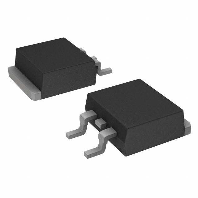
| 供应商器件封装 | SOT-223 |
| 典型关闭延迟时间 | 20 ns |
| 功率-最大值 | 2.8W |
| 功率耗散 | 2.8 W |
| 包装 | 管件 |
| 商标 | International Rectifier |
| 安装类型 | 表面贴装 |
| 安装风格 | SMD/SMT |
| 导通电阻 | 185 mOhms |
| 封装 | Tube |
| 封装/外壳 | TO-261-4,TO-261AA |
| 封装/箱体 | SOT-223-3 |
| 工厂包装数量 | 80 |
| 晶体管极性 | N-Channel |
| 最大工作温度 | + 150 C |
| 最小工作温度 | - 55 C |
| 栅极电荷Qg | 12 nC |
| 标准包装 | 80 |
| 汲极/源极击穿电压 | 150 V |
| 漏极连续电流 | 2.6 A |
| 漏源极电压(Vdss) | 150V |
| 电流-连续漏极(Id)(25°C时) | 2.6A (Ta) |
| 通道模式 | Enhancement |
| 配置 | Single Dual Drain |
| 闸/源击穿电压 | 30 V |


- 商务部:美国ITC正式对集成电路等产品启动337调查
- 曝三星4nm工艺存在良率问题 高通将骁龙8 Gen1或转产台积电
- 太阳诱电将投资9.5亿元在常州建新厂生产MLCC 预计2023年完工
- 英特尔发布欧洲新工厂建设计划 深化IDM 2.0 战略
- 台积电先进制程称霸业界 有大客户加持明年业绩稳了
- 达到5530亿美元!SIA预计今年全球半导体销售额将创下新高
- 英特尔拟将自动驾驶子公司Mobileye上市 估值或超500亿美元
- 三星加码芯片和SET,合并消费电子和移动部门,撤换高东真等 CEO
- 三星电子宣布重大人事变动 还合并消费电子和移动部门
- 海关总署:前11个月进口集成电路产品价值2.52万亿元 增长14.8%


PDF Datasheet 数据手册内容提取
(cid:2)(cid:3)(cid:1)(cid:4)(cid:1)(cid:5)(cid:6)(cid:7)(cid:6)(cid:8)(cid:9) IRFL4315PbF HEXFET(cid:1)(cid:1)Power MOSFET Applications V R max I DSS DS(on) D (cid:1) High frequency DC-DC converters 150V 185m(cid:1)@V = 10V 2.6A GS Benefits (cid:1) Low Gate to Drain Charge to Reduce Switching Losses (cid:1) Fully Characterized Capacitance Including Effective C to Simplify Design, (See OSS App. Note AN1001) SOT-223 (cid:1) Fully Characterized Avalanche Voltage and Current (cid:1) Lead-Free Absolute Maximum Ratings Parameter Max. Units I @ T = 25°C Continuous Drain Current, V @ 10V 2.6 D A GS I @ T = 70°C Continuous Drain Current, V @ 10V 2.1 A D A GS I Pulsed Drain Current (cid:2) 21 DM P @T = 25°C Power Dissipation(cid:3) 2.8 W D A Linear Derating Factor 0.02 W/°C V Gate-to-Source Voltage ± 30 V GS dv/dt Peak Diode Recovery dv/dt (cid:4) 6.3 V/ns T Operating Junction and -55 to + 150 J TSTG Storage Temperature Range °C Soldering Temperature, for 10 seconds 300 (1.6mm from case ) Thermal Resistance Symbol Parameter Typ. Max. Units RθJA Junction-to-Ambient (PCB Mount, steady state)(cid:1) ––– 45 °C/W Notes(cid:1)(cid:1)(cid:2)through (cid:3) are on page 8 www.irf.com 1 09/22/10
IRFL4315PbF Static @ T = 25°C (unless otherwise specified) J Parameter Min. Typ. Max. Units Conditions V(BR)DSS Drain-to-Source Breakdown Voltage 150 ––– ––– V VGS = 0V, ID = 250µA ∆V(BR)DSS/∆TJ Breakdown Voltage Temp. Coefficient ––– 0.19 ––– V/°C Reference to 25°C, ID = 1mA (cid:6) RDS(on) Static Drain-to-Source On-Resistance ––– ––– 185 mΩ VGS = 10V, ID = 1.6A(cid:5)(cid:6) VGS(th) Gate Threshold Voltage 3.0 ––– 5.0 V VDS = VGS, ID = 250µA IDSS Drain-to-Source Leakage Current ––– ––– 25 µA VDS = 150V, VGS = 0V ––– ––– 250 VDS = 120V, VGS = 0V, TJ = 125°C I Gate-to-Source Forward Leakage ––– ––– 100 nA VGS = 30V GSS Gate-to-Source Reverse Leakage ––– ––– -100 VGS = -30V Dynamic @ T = 25°C (unless otherwise specified) J Parameter Min. Typ. Max. Units Conditions gfs Forward Transconductance 3.5 ––– ––– S VDS = 50V, ID = 1.6A Qg Total Gate Charge ––– 12 19 ID = 1.6A Qgs Gate-to-Source Charge ––– 2.1 3.1 nC VDS = 120V Qgd Gate-to-Drain ("Miller") Charge ––– 6.8 10 VGS = 10V td(on) Turn-On Delay Time ––– 8.4 ––– VDD = 75V tr Rise Time ––– 21 ––– ns ID = 1.6A td(off) Turn-Off Delay Time ––– 20 ––– RG = 15Ω tf Fall Time ––– 19 ––– VGS = 10V(cid:5)(cid:6) Ciss Input Capacitance ––– 420 ––– VGS = 0V Coss Output Capacitance ––– 100 ––– VDS = 25V Crss Reverse Transfer Capacitance ––– 25 ––– pF ƒ = 1.0MHz Coss Output Capacitance ––– 720 ––– VGS = 0V, VDS = 1.0V, ƒ = 1.0MHz Coss Output Capacitance ––– 48 ––– VGS = 0V, VDS = 120V, ƒ = 1.0MHz Coss eff. Effective Output Capacitance ––– 98 ––– VGS = 0V, VDS = 0V to 120V (cid:7) Avalanche Characteristics Parameter Typ. Max. Units E Single Pulse Avalanche Energy(cid:8) ––– 38 mJ AS I Avalanche Current(cid:2) ––– 3.1 A AR Diode Characteristics Parameter Min. Typ. Max. Units Conditions IS Continuous Source Current ––– ––– 2.6 MOSFET symbol D (Body Diode) (cid:1) showing the ISM Pulsed Source Current integral reverse G ––– ––– 21 (Body Diode) (cid:2) p-n junction diode. S VSD Diode Forward Voltage ––– ––– 1.5 V TJ = 25°C, IS = 2.1A, VGS = 0V(cid:5)(cid:6) trr Reverse Recovery Time ––– 61 91 ns TJ = 25°C, IF = 1.6A Qrr Reverse RecoveryCharge ––– 160 240 nC di/dt = 100A/µs(cid:1)(cid:6) 2 www.irf.com
IRFL4315PbF 100 100 VGS VGS TOP 15V TOP 15V 12V 12V 10V 10V A) 8.0V A) 8.0V uenr(r t 10 B O T T O M 7665....0505VVVV uenrr(t 10 B O T T O M 7665....0505VVVV C C e e c c ur 1 5.5V ur 5.5V o o S S o- o- n-t n-t 1 ai ai Dr 0.1 Dr ,D , D I I 20µs PULSE WIDTH 20µs PULSE WIDTH Tj = 25°C Tj = 150°C 0.01 0.1 0.1 1 10 100 0.1 1 10 100 VDS, Drain-to-Source Voltage (V) VDS, Drain-to-Source Voltage (V) Fig 1. Typical Output Characteristics Fig 2. Typical Output Characteristics 100.00 2.5 ID= 2.6A ) Α ( 2.0 Cueuencrrr t 10.00 TJ = 150°C On Resistance malized) 1.5 Soo- urce (Nor 1.0 Dnar-, tiD TJ = 25°C Drain-to-So 0.5 I 1.00 V20DµSs =P U50LVSE WIDTH R , DS(on) 0.0 V GS=10V -60 -40 -20 0 20 40 60 80 100 120 140 160 5.0 6.0 7.0 8.0 9.0 10.0 T J , Junction Temperature ( ° C) V , Gate-to-Source Voltage (V) GS Fig 3. Typical Transfer Characteristics Fig 4. Normalized On-Resistance Vs. Temperature www.irf.com 3
IRFL4315PbF 10000 12 VGS = 0V, f = 1 MHZ ID= 1.6A Ciss = Cgs + Cgd, Cds SHORTED CCrossss = = CCgdds + Cgd Vge() 10 VVDDSS== 17250VV Fanepacc()ti1000 Ciss VSaeooucr tl 68 VDS= 30V p o- CCa, 100 Coss ae-tt 4 G , S G 2 C V rss FOR TEST CIRCUIT SEE FIGURE 13 10 0 1 10 100 1000 0 2 4 6 8 10 12 14 VDS, Drain-to-Source Voltage (V) QG Total Gate Charge (nC) Fig 5. Typical Capacitance Vs. Fig 6. Typical Gate Charge Vs. Drain-to-Source Voltage Gate-to-Source Voltage 100 100 OPERATION IN THIS AREA LIMITED BY RDS(on) A) nt (A) 10 T J = 150 ° C Cuenrr(t 10 Reverse Drain Curre 1 T J = 25 ° C DSanoouecr--rt i 1 110m0sµescec I , SD I, D Tc = 25°C 10msec Tj = 150°C Single Pulse V G S = 0 V 0.1 0.1 0.0 0.5 1.0 1.5 2.0 2.5 1 10 100 1000 V S D ,Source-to-Drain Voltage (V) V , Drain-to-Source Voltage (V) DS Fig 7. Typical Source-Drain Diode Fig 8. Maximum Safe Operating Area Forward Voltage 4 www.irf.com
IRFL4315PbF 3.0 (cid:3) (cid:1) (cid:2) (cid:1)(cid:2) 2.5 (cid:2) (cid:21)(cid:2) (cid:4)(cid:5)(cid:6)(cid:5)(cid:7)(cid:5) (cid:3) (cid:21) 2.0 +(cid:2) A) - (cid:1)(cid:1) ent ( (cid:8)(cid:9)(cid:2) urr 1.5 C (cid:3)(cid:4)(cid:5)(cid:6)(cid:7)(cid:8)(cid:9)(cid:10)(cid:11)(cid:12)(cid:13)(cid:8)≤ 1 (cid:14)(cid:6) n (cid:1)(cid:4)(cid:12)(cid:15)(cid:8)(cid:16)(cid:17)(cid:18)(cid:12)(cid:19)(cid:20)(cid:8)≤ 0.1 % ai Dr I , D 1.0 Fig 10a. Switching Time Test Circuit 0.5 VDS 90% 0.0 25 50 75 100 125 150 T , Ambient Tempe°rature (°C) A 10% Fig 9. Maximum Drain Current Vs. VGS Ambient Temperature td(on) tr td(off) tf Fig 10b. Switching Time Waveforms 100 Z )thJA D = 0.50 ( 10 0.20 0.10 e s on 0.05 p es PDM mal R 1 0.02 t1 her 0.01 t2 T SINGLE PULSE Notes: (THERMAL RESPONSE) 1. Duty factor D = t 1 / t 2 2. Peak T J=PDM x Z thJA + TA 0.1 0.00001 0.0001 0.001 0.01 0.1 1 10 100 t 1 , Rectangular Pulse Duration (sec) Fig 11. Maximum Effective Transient Thermal Impedance, Junction-to-Case www.irf.com 5
IRFL4315PbF Ω) 240 Ω) 4000 m m ce ( 220 ec( 3500 n n a a essit 200 essti 3000 R R n n 2500 O O e 180 VGS = 10V e ucr ucr 2000 So 160 So Dano, r--itn) 112400 Danor--t , in)11055000000 ID = 2.6A So( So( RD 100 RD 0 0 5 10 15 20 25 4.5 6.0 7.5 9.0 10.5 12.0 13.5 15.0 ID , Drain Current (A) VGS, Gate -to -Source Voltage (V) Fig 12. On-Resistance Vs. Drain Current Fig 13. On-Resistance Vs. Gate Voltage CurrentRegulator SameTypeasD.U.T. (cid:2) QG 50KΩ (cid:1)(cid:2) 12V .2µF .3µF QGS QGD + D.U.T. -VDS VG 100 VGS ID 3mA Charge TOP 1.4A 2.5A CurrentIGSamplingReIDsistors 80 BOTTOM 3.1A J) m Fig 14a&b. Basic Gate Charge Test Circuit y ( g and Waveform er 60 n E e h c n a al 40 v A 15V e s ul V(BR)DSS P tp VDS L DRIVER gle 20 n Si RG IADS.U.T +-VDDA E , AS 20V 0 tp 0.01Ω 25 50 75 100 125 150 IAS Starting Tj, Junction Temperature ( ° C) Fig 15c. Maximum Avalanche Energy Fig 15a&b. Unclamped Inductive Test circuit Vs. Drain Current and Waveforms 6 www.irf.com
IRFL4315PbF (cid:1)(cid:2)(cid:3)(cid:4)(cid:5)(cid:5)(cid:6)(cid:7)(cid:8)(cid:3)(cid:2)(cid:4)(cid:5)(cid:9)(cid:10)(cid:11)(cid:11)(cid:12)(cid:7)(cid:13)(cid:14)(cid:15)(cid:16)(cid:14)(cid:17)(cid:18)(cid:7)(cid:2)(cid:19)(cid:20)(cid:21)(cid:22)(cid:23)(cid:18) (cid:4)(cid:10)(cid:11)(cid:12)(cid:13)(cid:14)(cid:10)(cid:15)(cid:13)(cid:14)(cid:16)(cid:17)(cid:18)(cid:12)(cid:16)(cid:14)(cid:19)(cid:15)(cid:20)(cid:13)(cid:16)(cid:10)(cid:13)(cid:16)(cid:11)(cid:10)(cid:21)(cid:10)(cid:11)(cid:12)(cid:22)(cid:12)(cid:18)(cid:14)(cid:16)(cid:23)(cid:10)(cid:13)(cid:24)(cid:19)(cid:12)(cid:14)(cid:25) (cid:1)(cid:2)(cid:3)(cid:4)(cid:5)(cid:5)(cid:6)(cid:7)(cid:8)(cid:3)(cid:2)(cid:4)(cid:5)(cid:9)(cid:10)(cid:11)(cid:11)(cid:12)(cid:7)(cid:13)(cid:14)(cid:24)(cid:20)(cid:7)(cid:25)(cid:14)(cid:24)(cid:16)(cid:22)(cid:23)(cid:17)(cid:7)(cid:26)(cid:23)(cid:27)(cid:28)(cid:24)(cid:29)(cid:14)(cid:20)(cid:22)(cid:28)(cid:23) HEXFET PRODUCT MARKING THIS IS AN IRFL014 PART NUMBER LOT CODE INTERNATIONAL RECTIFIER FL014 AXXXX LOGO 314P DATE CODE A = ASSEMBLY SITE (YYWW) CODE YY = YEAR TOP WW = WEEK BOTTOM P = DESIGNATES LEAD-FREE PRODUCT (OPTIONAL) Notes: 1.For an Automotive Qualified version of this part please seehttp://www.irf.com/product-info/auto/ 2.For the most current drawing please refer to IR website at http://www.irf.com/package/ www.irf.com 7
IRFL4315PbF (cid:1)(cid:2)(cid:3)(cid:4)(cid:5)(cid:5)(cid:6)(cid:7)(cid:8)(cid:3)(cid:2)(cid:4)(cid:5)(cid:9)(cid:10)(cid:11)(cid:11)(cid:12)(cid:7)(cid:3)(cid:14)(cid:30)(cid:18)(cid:7)(cid:31)(cid:7) (cid:18)(cid:18)(cid:21)(cid:7)(cid:26)(cid:23)(cid:27)(cid:28)(cid:24)(cid:29)(cid:14)(cid:20)(cid:22)(cid:28)(cid:23) (cid:4)(cid:10)(cid:11)(cid:12)(cid:13)(cid:14)(cid:10)(cid:15)(cid:13)(cid:14)(cid:16)(cid:17)(cid:18)(cid:12)(cid:16)(cid:14)(cid:19)(cid:15)(cid:20)(cid:13)(cid:16)(cid:10)(cid:13)(cid:16)(cid:11)(cid:10)(cid:21)(cid:10)(cid:11)(cid:12)(cid:22)(cid:12)(cid:18)(cid:14)(cid:16)(cid:23)(cid:10)(cid:13)(cid:24)(cid:19)(cid:12)(cid:14)(cid:25) 2.05 (.080) 43..1900 ((..116514)) 11..8655 ((..007625)) 00..3255 ((..001130)) TR 1.95 (.077) 7.55 (.297) 7.45 (.294) 16.30 (.641) 7.60 (.299) 15.70 (.619) 7.40 (.292) 1.60 (.062) 1.50 (.059) TYP. FEED DIRECTION 7.10 (.279) 2.30 (.090) 6.90 (.272) 2.10 (.083) 12.10 (.475) 11.90 (.469) NOTES : 1. CONTROLLING DIMENSION: MILLIMETER. 2. OUTLINE CONFORMS TO EIA-481 & EIA-541. 3. EACH O330.00 (13.00) REEL CONTAINS 2,500 DEVICES. 13.20 (.519) 15.40 (.607) 12.80 (.504) 11.90 (.469) 4 330.00 50.00 (1.969) (13.000) MIN. MAX. NOTES : 18.40 (.724) 1. OUTLINE COMFORMS TO EIA-418-1. MAX. 2. CONTROLLING DIMENSION: MILLIMETER.. 14.40 (.566) 4 3. DIMENSION MEASURED @ HUB. 12.40 (.488) 4. INCLUDES FLANGE DISTORTION @ OUTER EDGE. 3 (cid:1)(cid:2)(cid:3)(cid:4)(cid:5)(cid:6) (cid:2)(cid:16)Repetitive rating; pulse width limited by (cid:1) When mounted on 1 inch square copper board. max. junction temperature. (cid:5) Coss eff. is a fixed capacitance that gives the same charging time (cid:3) (cid:16)Starting TJ = 25°C, L = 7.8mH as Coss while VDS is rising from 0 to 80% VDSS. RG = 25Ω, IAS = 3.1A. (cid:6)ISD ≤ 1.6A, di/dt ≤ 230A/µs, VDD ≤ V(BR)DSS, (cid:4) Pulse width ≤ 400µs; duty cycle ≤ 2%. T ≤ 150°C. J Data and specifications subject to change without notice. This product has been designed and qualified for the Industrial market. Qualification Standards can be found on IR’s Web site. IR WORLD HEADQUARTERS: 233 Kansas St., El Segundo, California 90245, USA Tel: (310) 252-7105 TAC Fax: (310) 252-7903 Visit us at www.irf.com for sales contact information.09/2010 8 www.irf.com
Mouser Electronics Authorized Distributor Click to View Pricing, Inventory, Delivery & Lifecycle Information: I nfineon: IRFL4315PBF IRFL4315TRPBF