ICGOO在线商城 > 分立半导体产品 > 晶体管 - FET,MOSFET - 单 > IRFD9120PBF
 Datasheet下载
- 型号: IRFD9120PBF
- 制造商: Vishay
- 库位|库存: xxxx|xxxx
- 要求:
| 数量阶梯 | 香港交货 | 国内含税 |
| +xxxx | $xxxx | ¥xxxx |
查看当月历史价格
查看今年历史价格
IRFD9120PBF产品简介:
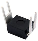
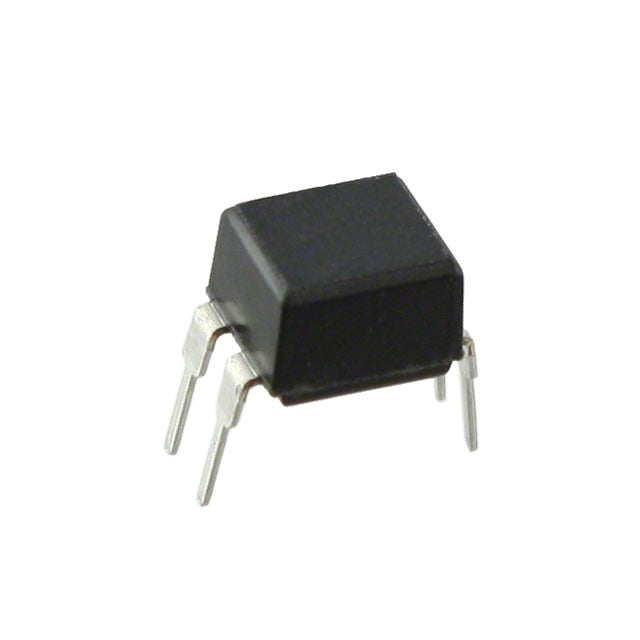
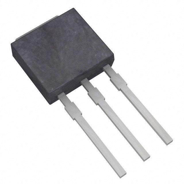
ICGOO电子元器件商城为您提供IRFD9120PBF由Vishay设计生产,在icgoo商城现货销售,并且可以通过原厂、代理商等渠道进行代购。 IRFD9120PBF价格参考。VishayIRFD9120PBF封装/规格:晶体管 - FET,MOSFET - 单, 通孔 P 沟道 100V 1A(Ta) 1.3W(Ta) 4-DIP,Hexdip,HVMDIP。您可以下载IRFD9120PBF参考资料、Datasheet数据手册功能说明书,资料中有IRFD9120PBF 详细功能的应用电路图电压和使用方法及教程。
| 参数 | 数值 |
| 产品目录 | |
| ChannelMode | Enhancement |
| 描述 | MOSFET P-CH 100V 1A 4-DIPMOSFET P-Chan 100V 1.0 Amp |
| 产品分类 | FET - 单分离式半导体 |
| FET功能 | 标准 |
| FET类型 | MOSFET P 通道,金属氧化物 |
| Id-ContinuousDrainCurrent | 1 A |
| Id-连续漏极电流 | 1 A |
| 品牌 | Vishay / Siliconix |
| 产品手册 | |
| 产品图片 |
|
| rohs | RoHS 合规性豁免无铅 / 符合限制有害物质指令(RoHS)规范要求 |
| 产品系列 | 晶体管,MOSFET,Vishay / Siliconix IRFD9120PBF- |
| 数据手册 | http://www.vishay.com/doc?91139 |
| 产品型号 | IRFD9120PBF |
| Pd-PowerDissipation | 1300 mW |
| Pd-功率耗散 | 1.3 W |
| RdsOn-Drain-SourceResistance | 600 mOhms |
| RdsOn-漏源导通电阻 | 600 mOhms |
| Vds-Drain-SourceBreakdownVoltage | 100 V |
| Vds-漏源极击穿电压 | - 100 V |
| Vgs-Gate-SourceBreakdownVoltage | +/- 20 V |
| Vgs-栅源极击穿电压 | 20 V |
| 上升时间 | 29 ns |
| 下降时间 | 29 ns |
| 不同Id时的Vgs(th)(最大值) | 4V @ 250µA |
| 不同Vds时的输入电容(Ciss) | 390pF @ 25V |
| 不同Vgs时的栅极电荷(Qg) | 18nC @ 10V |
| 不同 Id、Vgs时的 RdsOn(最大值) | 600 毫欧 @ 600mA,10V |
| 产品目录绘图 |
|
| 产品目录页面 | |
| 产品种类 | MOSFET |
| 供应商器件封装 | 4-DIP,Hexdip,HVMDIP |
| 其它名称 | *IRFD9120PBF |
| 典型关闭延迟时间 | 21 ns |
| 功率-最大值 | 1.3W |
| 功率耗散 | 1300 mW |
| 包装 | 管件 |
| 商标 | Vishay / Siliconix |
| 安装类型 | 通孔 |
| 安装风格 | Through Hole |
| 导通电阻 | 600 mOhms |
| 封装 | Tube |
| 封装/外壳 | 4-DIP(0.300",7.62mm) |
| 封装/箱体 | HexDIP-4 |
| 工厂包装数量 | 2500 |
| 晶体管极性 | P-Channel |
| 最大工作温度 | + 150 C |
| 最小工作温度 | - 55 C |
| 标准包装 | 2,500 |
| 汲极/源极击穿电压 | 100 V |
| 漏极连续电流 | 1 A |
| 漏源极电压(Vdss) | 100V |
| 电流-连续漏极(Id)(25°C时) | 1A (Ta) |
| 通道模式 | Enhancement |
| 配置 | Single Dual Drain |
| 闸/源击穿电压 | +/- 20 V |


- 商务部:美国ITC正式对集成电路等产品启动337调查
- 曝三星4nm工艺存在良率问题 高通将骁龙8 Gen1或转产台积电
- 太阳诱电将投资9.5亿元在常州建新厂生产MLCC 预计2023年完工
- 英特尔发布欧洲新工厂建设计划 深化IDM 2.0 战略
- 台积电先进制程称霸业界 有大客户加持明年业绩稳了
- 达到5530亿美元!SIA预计今年全球半导体销售额将创下新高
- 英特尔拟将自动驾驶子公司Mobileye上市 估值或超500亿美元
- 三星加码芯片和SET,合并消费电子和移动部门,撤换高东真等 CEO
- 三星电子宣布重大人事变动 还合并消费电子和移动部门
- 海关总署:前11个月进口集成电路产品价值2.52万亿元 增长14.8%


PDF Datasheet 数据手册内容提取
IRFD9120, SiHFD9120 Vishay Siliconix Power MOSFET FEATURES PRODUCT SUMMARY • Dynamic dV/dt Rating V (V) - 100 DS • Repetitive Avalanche Rated Available RDS(on) () VGS = - 10 V 0.60 RoHS* • For Automatic Insertion Qg (Max.) (nC) 18 COMPLIANT Q (nC) 3.0 • End Stackable gs Q (nC) 9.0 • P-Channel gd Configuration Single • 175 °C Operating Temperature S • Fast Switching • Compliant to RoHS Directive 2002/95/EC HVMDIP DESCRIPTION G Third generation Power MOSFETs from Vishay provide the designer with the best combination of fast switching, ruggedized device design, low on-resistance and S G cost-effectiveness. D D The 4 pin DIP package is a low cost machine-insertiable case style which can be stacked in multiple combinations on P-Channel MOSFET standard 0.1" pin centers. The dual drain serves as a thermal link to the mounting surface for power dissipation levels up to 1 W. ORDERING INFORMATION Package HVMDIP IRFD9120PbF Lead (Pb)-free SiHFD9120-E3 IRFD9120 SnPb SiHFD9120 ABSOLUTE MAXIMUM RATINGS (T = 25 °C, unless otherwise noted) A PARAMETER SYMBOL LIMIT UNIT Drain-Source Voltage V - 100 DS V Gate-Source Voltage V ± 20 GS T = 25 °C - 1.0 A Continuous Drain Current V at - 10 V I GS D T = 100 °C - 0.70 A A Pulsed Drain Currenta I - 8.0 DM Linear Derating Factor 0.0083 W/°C Single Pulse Avalanche Energyb E 140 mJ AS Repetitive Avalanche Currenta I - 1.0 A AR Repetitive Avalanche Energya E 0.13 mJ AR Maximum Power Dissipation T = 25 °C P 1.3 W A D Peak Diode Recovery dV/dtc dV/dt - 5.5 V/ns Operating Junction and Storage Temperature Range T , T - 55 to + 175 J stg °C Soldering Recommendations (Peak Temperature) for 10 s 300d Notes a. Repetitive rating; pulse width limited by maximum junction temperature (see fig. 11). b. VDD = - 25 V, starting TJ = 25 °C, L = 52 mH, Rg = 25 , IAS = - 2.0 A (see fig. 12). c. ISD - 6.8 A, dI/dt 110 A/μs, VDD VDS, TJ 175 °C. d. 1.6 mm from case. * Pb containing terminations are not RoHS compliant, exemptions may apply Document Number: 91139 www.vishay.com S10-2464-Rev. D, 25-Oct-10 1
IRFD9120, SiHFD9120 Vishay Siliconix THERMAL RESISTANCE RATINGS PARAMETER SYMBOL TYP. MAX. UNIT Maximum Junction-to-Ambient R - 120 °C/W thJA SPECIFICATIONS (T = 25 °C, unless otherwise noted) J PARAMETER SYMBOL TEST CONDITIONS MIN. TYP. MAX. UNIT Static Drain-Source Breakdown Voltage V V = 0 V, I = - 250 μA - 100 - - V DS GS D VDS Temperature Coefficient VDS/TJ Reference to 25 °C, ID = - 1 mA - - 0.10 - V/°C Gate-Source Threshold Voltage V V = V , I = - 250 μA - 2.0 - - 4.0 V GS(th) DS GS D Gate-Source Leakage I V = ± 20 V - - ± 100 nA GSS GS V = - 100 V, V = 0 V - - - 100 DS GS Zero Gate Voltage Drain Current I μA DSS V = - 80 V, V = 0 V, T = 150 °C - - - 500 DS GS J Drain-Source On-State Resistance RDS(on) VGS = - 10 V ID = - 0.6 Ab - - 0.60 Forward Transconductance g V = - 50 V, I = - 0.60 Ab 0.71 - - S fs DS D Dynamic Input Capacitance C - 390 - iss V = 0 V GS Output Capacitance C V = - 25 V - 170 - pF oss DS f = 1.0 MHz, see fig. 5 Reverse Transfer Capacitance C - 45 - rss Total Gate Charge Q - - 18 g I = - 6.8 A, V = - 80 V Gate-Source Charge Q V = - 10 V D DS - - 3.0 nC gs GS see fig. 6 and 13b Gate-Drain Charge Q - - 9.0 gd Turn-On Delay Time t - 9.6 - d(on) Rise Time t - 29 - r VDD = - 50 V, ID = - 6.8 A ns Turn-Off Delay Time td(off) Rg = 18 , RD = 7.1 , see fig. 10b - 21 - Fall Time t - 25 - f Between lead, Internal Drain Inductance L D - 4.0 - D 6 mm (0.25") from package and center of nH G Internal Source Inductance L die contact - 6.0 - S S Drain-Source Body Diode Characteristics MOSFET symbol Continuous Source-Drain Diode Current IS showing the D - - - 1.0 integral reverse A G Pulsed Diode Forward Currenta I p - n junction diode - - - 8.0 SM S Body Diode Voltage V T = 25 °C, I = - 1.0 A, V = 0 Vb - - - 6.3 V SD J S GS Body Diode Reverse Recovery Time t - 98 200 ns rr T = 25 °C, I = - 6.8 A, dI/dt = 100 A/μsb J F Body Diode Reverse Recovery Charge Q - 0.33 0.66 μC rr Forward Turn-On Time t Intrinsic turn-on time is negligible (turn-on is dominated by L and L ) on S D Notes a. Repetitive rating; pulse width limited by maximum junction temperature (see fig. 11). b. Pulse width 300 μs; duty cycle 2 %. www.vishay.com Document Number: 91139 2 S10-2464-Rev. D, 25-Oct-10
IRFD9120, SiHFD9120 Vishay Siliconix TYPICAL CHARACTERISTICS (25 °C, unless otherwise noted) TA = 25 °C Fig. 1 - Typical Output Characteristics, T = 25 °C Fig. 3 - Typical Transfer Characteristics A TA = 175 °C Fig. 2 - Typical Output Characteristics, T = 175 °C Fig. 4 - Normalized On-Resistance vs. Temperature A Document Number: 91139 www.vishay.com S10-2464-Rev. D, 25-Oct-10 3
IRFD9120, SiHFD9120 Vishay Siliconix Fig. 5 - Typical Capacitance vs. Drain-to-Source Voltage Fig. 7 - Typical Source-Drain Diode Forward Voltage TA = 25 °C TJ = 175 °C SINGLE PULSE Fig. 6 - Typical Gate Charge vs. Gate-to-Source Voltage Fig. 8 - Maximum Safe Operating Area www.vishay.com Document Number: 91139 4 S10-2464-Rev. D, 25-Oct-10
IRFD9120, SiHFD9120 Vishay Siliconix R D V DS V GS D.U.T. R g - +VDD A) - 10 V ent ( DPuultsye f awcitdotrh ≤ ≤ 01. 1µ %s urr C n Fig. 10a - Switching Time Test Circuit ai Dr , D I t t t t d(on) r d(off) f V GS 10 % TA, Ambient Temperature (°C) 90 % V DS Fig. 9 - Maximum Drain Current vs. Ambient Temperature Fig. 10b - Switching Time Waveforms )A J h Zt e ( s n o p s e R al m er h T t1, Rectangular Pulse Duration (s) Fig. 11 - Maximum Effective Transient Thermal Impedance, Junction-to-Ambient Document Number: 91139 www.vishay.com S10-2464-Rev. D, 25-Oct-10 5
IRFD9120, SiHFD9120 Vishay Siliconix L I AS V DS Vary t to obtain p required I AS V DS R D.U.T. G - +V DD V I DD AS t p - 10 V t 0.01 Ω p V DS Fig. 12a - Unclamped Inductive Test Circuit Fig. 12b - Unclamped Inductive Waveforms Fig. 12c - Maximum Avalanche Energy vs. Drain Current Current regulator Same type as D.U.T. 50 kΩ Q G - 10 V 12 V 0.2 µF 0.3 µF Q Q - GS GD V D.U.T. + DS VG VGS - 3 mA Charge I I G D Current sampling resistors Fig. 13a - Basic Gate Charge Waveform Fig. 13b - Gate Charge Test Circuit www.vishay.com Document Number: 91139 6 S10-2464-Rev. D, 25-Oct-10
IRFD9120, SiHFD9120 Vishay Siliconix Peak Diode Recovery dV/dt Test Circuit D.U.T. + Circuit layout considerations (cid:129) Low stray inductance (cid:129) Ground plane (cid:129) Low leakage inductance current transformer - + - + - Rg (cid:129) dV/dt controlled by Rg + (cid:129)(cid:129) IDSD.U c.oTn. t-r odlelevdic be yu dnduteyr ftaecsttor “D” - VDD Note (cid:129) Compliment N-Channel of D.U.T. for driver Driver gate drive P.W. Period D = P.W. Period V = - 10 Va GS D.U.T. l waveform SD Reverse recovery Body diode forward current current dI/dt D.U.T. V waveform DS Diode recovery dV/dt V DD Re-applied voltage Body diode forward drop Inductor current Ripple ≤ 5 % ISD Note a. V = - 5 V for logic level and - 3 V drive devices GS Fig. 14 - For P-Channel Vishay Siliconix maintains worldwide manufacturing capability. Products may be manufactured at one of several qualified locations. Reliability data for Silicon Technology and Package Reliability represent a composite of all qualified locations. For related documents such as package/tape drawings, part marking, and reliability data, see www.vishay.com/ppg?91139. Document Number: 91139 www.vishay.com S10-2464-Rev. D, 25-Oct-10 7
Package Information Vishay Siliconix HVM DIP (High voltage) 0.248 [6.29] 0.240 [6.10] 0.043 [1.09] 0.197 [5.00] 0.035 [0.89] 0.133 [3.37] 0.189 [4.80] 0.125 [3.18] 0.180 [4.57] 0.160 [4.06] 0.094 [2.38] A L 0.086 [2.18] 0.160 [4.06] 0.140 [3.56] 0° to 15° 0.017 [0.43] 2 x 0.045 [1.14] 0.013 [0.33] 2 x 0.035 [0.89] 0.024 [0.60] 4 x E min. 0.020 [0.51] 0.100 [2.54] typ. E max. INCHES MILLIMETERS DIM. MIN. MAX. MIN. MAX. A 0.310 0.330 7.87 8.38 E 0.300 0.425 7.62 10.79 L 0.270 0.290 6.86 7.36 ECN: X10-0386-Rev. B, 06-Sep-10 DWG: 5974 Note 1. Package length does not include mold flash, protrusions or gate burrs. Package width does not include interlead flash or protrusions. Document Number: 91361 www.vishay.com Revision: 06-Sep-10 1
Legal Disclaimer Notice www.vishay.com Vishay Disclaimer ALL PRODUCT, PRODUCT SPECIFICATIONS AND DATA ARE SUBJECT TO CHANGE WITHOUT NOTICE TO IMPROVE RELIABILITY, FUNCTION OR DESIGN OR OTHERWISE. Vishay Intertechnology, Inc., its affiliates, agents, and employees, and all persons acting on its or their behalf (collectively, “Vishay”), disclaim any and all liability for any errors, inaccuracies or incompleteness contained in any datasheet or in any other disclosure relating to any product. Vishay makes no warranty, representation or guarantee regarding the suitability of the products for any particular purpose or the continuing production of any product. To the maximum extent permitted by applicable law, Vishay disclaims (i) any and all liability arising out of the application or use of any product, (ii) any and all liability, including without limitation special, consequential or incidental damages, and (iii) any and all implied warranties, including warranties of fitness for particular purpose, non-infringement and merchantability. Statements regarding the suitability of products for certain types of applications are based on Vishay’s knowledge of typical requirements that are often placed on Vishay products in generic applications. Such statements are not binding statements about the suitability of products for a particular application. It is the customer’s responsibility to validate that a particular product with the properties described in the product specification is suitable for use in a particular application. Parameters provided in datasheets and / or specifications may vary in different applications and performance may vary over time. All operating parameters, including typical parameters, must be validated for each customer application by the customer’s technical experts. Product specifications do not expand or otherwise modify Vishay’s terms and conditions of purchase, including but not limited to the warranty expressed therein. Except as expressly indicated in writing, Vishay products are not designed for use in medical, life-saving, or life-sustaining applications or for any other application in which the failure of the Vishay product could result in personal injury or death. Customers using or selling Vishay products not expressly indicated for use in such applications do so at their own risk. Please contact authorized Vishay personnel to obtain written terms and conditions regarding products designed for such applications. No license, express or implied, by estoppel or otherwise, to any intellectual property rights is granted by this document or by any conduct of Vishay. Product names and markings noted herein may be trademarks of their respective owners. © 2017 VISHAY INTERTECHNOLOGY, INC. ALL RIGHTS RESERVED Revision: 08-Feb-17 1 Document Number: 91000
Mouser Electronics Authorized Distributor Click to View Pricing, Inventory, Delivery & Lifecycle Information: V ishay: IRFD9120 IRFD9120PBF