ICGOO在线商城 > IR3822AMTRPBF
- 型号: IR3822AMTRPBF
- 制造商: International Rectifier
- 库位|库存: xxxx|xxxx
- 要求:
| 数量阶梯 | 香港交货 | 国内含税 |
| +xxxx | $xxxx | ¥xxxx |
查看当月历史价格
查看今年历史价格
IR3822AMTRPBF产品简介:
ICGOO电子元器件商城为您提供IR3822AMTRPBF由International Rectifier设计生产,在icgoo商城现货销售,并且可以通过原厂、代理商等渠道进行代购。 提供IR3822AMTRPBF价格参考以及International RectifierIR3822AMTRPBF封装/规格参数等产品信息。 你可以下载IR3822AMTRPBF参考资料、Datasheet数据手册功能说明书, 资料中有IR3822AMTRPBF详细功能的应用电路图电压和使用方法及教程。
| 参数 | 数值 |
| 产品目录 | 集成电路 (IC) |
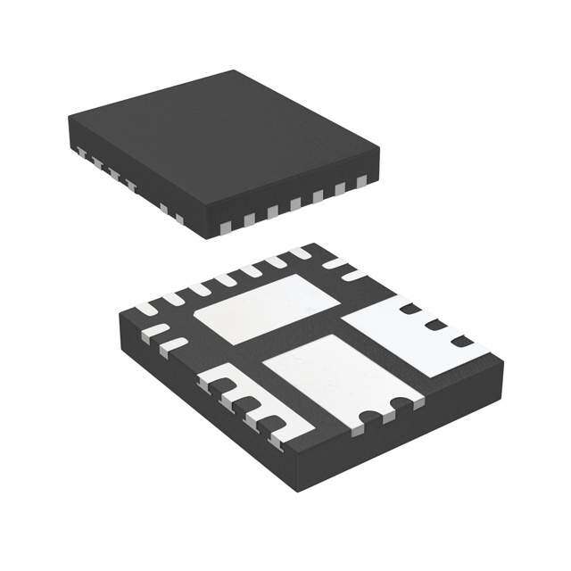
| 描述 | IC REG BUCK SYNC ADJ 6A 15QFN |
| 产品分类 | |
| 品牌 | International Rectifier |
| 数据手册 | |
| 产品图片 |
|
| 产品型号 | IR3822AMTRPBF |
| PCN组件/产地 | |
| PWM类型 | 电压模式 |
| rohs | 无铅 / 符合限制有害物质指令(RoHS)规范要求 |
| 产品系列 | SupIRBuck™ |
| 产品目录页面 | |
| 供应商器件封装 | PQFN(5x6) |
| 其它名称 | IR3822AMTRPBFTR |
| 包装 | 带卷 (TR) |
| 同步整流器 | 是 |
| 安装类型 | 表面贴装 |
| 封装/外壳 | 15-PowerVQFN |
| 工作温度 | -40°C ~ 125°C |
| 标准包装 | 4,000 |
| 电压-输入 | 2.5 V ~ 21 V |
| 电压-输出 | 0.6 V ~ 12 V |
| 电流-输出 | 6A |
| 类型 | 降压(降压) |
| 输出数 | 1 |
| 输出类型 | 可调式 |
| 频率-开关 | 300kHz |

PDF Datasheet 数据手册内容提取
PD-60345 IR3822AMPbF SupIRBuck TM HIGHLY INTEGRATED 6A WIDE-INPUT VOLTAGE, SYNCHRONOUS BUCK REGULATOR Features Description • Wide Input Voltage Range 2.5V to 21V The IR3822A SupIRBuckTM is an easy-to-use, • Wide Output Voltage Range 0.6V to 12V fully integrated and highly efficient DC/DC • Continuous 6A Load Capability • 300kHz High Frequency Operation regulator. The onboard switching controller and • Programmable Over-Current Protection MOSFETs make the IR3822A a space-efficient • Programmable PGood Output solution, providing accurate power delivery for • Hiccup Current Limit low output voltage applications. • Precision Reference Voltage (0.6V) The IR3822A operates from a single 4.5V to 14V • Programmable Soft-Start input supply and generates an output voltage • Pre-Bias Start-up adjustable from 0.6V to 0.8*Vin at loads up to 6A. • Thermal Protection A versatile regulator offering programmability of • Thermally Enhanced Package startup time, power good threshold and current • Small Size 5mmx6mm QFN limit, the IR3822A’s fixed 300kHz switching • Pb-Free (RoHS Compliant) frequency allows the use of small external Applications components. • Distributed Point-of-Loads The IR3822A also features important protection • Server and Workstations functions, such as Pre-Bias startup, hiccup • Embedded Systems current limit and thermal shutdown to provide the • Storage Systems required system level security in the event of fault • DDR Applications conditions. • Graphics Cards • Game Consoles • Computing Peripheral Voltage Regulators Fig. 1. Typical application diagram 11/04/08 1
PD-60345 IR3822AMPbF ABSOLUTE MAXIMUM RATINGS (Voltages referenced to GND) • V Supply Voltage -0.3V to 24V IN • Vcc Supply Voltage -0.3V to 16V • Vc Supply Voltage -0.3V to 30V • SW -0.3V to 30V • PGood -0.3V to 16V • Fb,COMP,SS,Vsns -0.3V to 3.5V • OCSet 10mA • AGnd to PGnd -0.3V to +0.3V • Storage Temperature Range -65°C To 150°C • Operating Junction Temperature Range -40°C To 150°C • ESD Classification JEDEC, JESD22-A114 • Moisture Sensitivity Level JEDEC Level 3 @ 260oC Caution: Stresses beyond those listed under “Absolute Maximum Rating”may cause permanent damage to the device. These are stress ratings only and functional operation of the device at these or any other conditions beyond those indicated in the operational sections of the specifications is not implied. Exposure to “Absolute Maximum Rating”conditions for extended periods may affect device reliability. PACKAGE INFORMATION 5mm x 6mm POWER QFN 10 12 11 V SW IN PGnd θ =35oC / W JA θ =2oC / W J-PCB 15 HG 13 9 PGood AGnd V 14 8 V C CC 1 2 3 4 5 6 7 Vsns FB COMP AGnd AGnd SS OCSet Fig. 2: Package outline (Top view) ORDERING INFORMATION PACKAGE PACKAGE PIN PARTS PER DESIGNATOR DESCRIPTION COUNTS REEL M IR3822AMTRPBF 15 4000 M IR3822AMTR1PBF 15 750 11/04/08 2
PD-60345 IR3822AMPbF Block Diagram Fig. 3. Simplified block diagram of the IR3822A. 11/04/08 3
PD-60345 IR3822AMPbF Pin Description Pin Name Description 1 Vsns PGood sense pin. Use two external resistors to program the power good threshold. 2 Fb Inverting input to the error amplifier. This pin is connected directly to the output of the regulator via resistor divider to set the output voltage and provide feedback to the error amplifier. 3 Comp Output of error amplifier. 4 AGnd Signal ground for internal reference and control circuitry. 5 AGnd Signal ground for internal reference and control circuitry. 6 SS/SD Soft start / shutdown. This pin provides user programmable soft-start function. Connect an external capacitor from this pin to signal ground (AGnd) to set the start up time of the output voltage. The converter can be shutdown by pulling this pin below 0.3V. 7 OCSet Current limit set point. A resistor from this pin to SW pin will set the current limit threshold. 8 V This pin provides biasing voltage for the internal blocks of the IC. It also CC powers the low side driver. A minimum of 0.1uF, high frequency capacitor must be connected from this pin to power ground (PGnd). 9 PGood Power Good status pin. Output is open collector. Connect a pull up resistor from this pin to Vcc. 10 PGnd Power Ground. This pin serves as a separated ground for the MOSFET drivers and should be connected to the system’s power ground plane. 11 SW Switch node. This pin is connected to the output inductor 12 V Input voltage connection pin IN 13 HG This pin is connected to the high side Mosfet gate. Connect a small capacitor from this pin to switch node (SW). 14 V This pin powers the high side driver and must be connected to a voltage C higher than input voltage. A minimum of 0.1uF high frequency capacitor must be connected from this pin to the power ground (PGnd). 15 AGnd Signal ground for internal reference and control circuitry. Pins 4, 5 and 15 need to be connected together on system board. 11/04/08 4
PD-60345 IR3822AMPbF Recommended Operating Conditions Symbol Definition Min Max Units V Input Voltage 2.5 21 in V Supply Voltage 4.5 14 cc V V Supply Voltage Vin + 5V 28 c V Output Voltage 0.6 12 o Io Note1 Output Current 0 6 A T Junction Temperature -40 125 oC j Electrical Specifications Unless otherwise specified, these specification apply over Vin=V =V =12V, 0oC<T(Ic)<105oC. cc c j Typical values are specified at T = 25oC. a Parameter Symbol Test Condition Min TYP MAX Units Power Loss Power Loss P Vcc=V =12V, Vc=24V, V=1.8V, 1.8 W loss in o I=6A, L=2.2uH, Note3 o MOSFET Rds(on) Top Switch Rds(on)_Top ID=6A, Tj(MOSFET)=25oC 18 23 mΩ Bottom Switch Rds(on)_Bot ID=6A, Tj(MOSFET)=25oC 18 23 Reference Voltage Feedback Voltage V 0.6 V FB Accuracy 0oC<Tj<105oC -1.35 +13.5 % -40oC<Tj<105oC, Note2 -1.5 +1.5 % Supply Current VCC Supply Current (Static) ICC(Static) SS=0V, No Switching 10 13 V Supply Current I SS=0V, No Switching 4.5 7 C C(Static) (Static) V Supply Current I SS=3V, V=24V, V =V =12V. 13 20 mA CC CC(Dynamic) c cc in (Dynamic) Vo=1.8V, Io=0A V Supply Current I SS=3V, V=24V, V =V =12V. 13 20 C C(Dynamic) c cc in (Dynamic) V=1.8V, Io=0A o Under Voltage Lockout V -Start-Threshold V _UVLO(R) Supply ramping up 4.0 4.4 CC CC V -Stop-Threshold V _UVLO(F) Supply ramping down 3.7 4.1 CC CC V -Hysteresis Supply ramping up and down 0.15 0.25 0.3 CC V -Start-Threshold V _UVLO(R) Supply ramping up 3.1 3.5 V C C V -Stop-Threshold V _UVLO(F) Supply ramping down 2.85 3.25 C C V -Hysteresis Supply ramping up and down 0.15 0.2 0.25 C 11/04/08 5
PD-60345 IR3822AMPbF Parameter SYM Test Condition Min TYP MAX Units Oscillator Frequency F 270 300 330 kHz S Ramp Amplitude V Note3 1.25 V ramp Min Pulse Width D Note3 80 ns min(ctrl) Max Duty Cycle D Fb=0V 80 % max Error Amplifier Input Bias Current I SS=3V -0.1 -0.5 FB1 Input Bias Current I SS=0V 20 35 50 FB2 μA Source/Sink Current I(source/Sink) 50 70 90 Transconductance gm 1000 1300 1600 μmho Soft Start/SD Soft Start Current ISS SS=0V 15 20 28 μA Shutdown Output SD 0.25 V Threshold Power Good Vsns Low Trip Point Vsns(trip) Vsns Ramping Down 0.35 0.38 0.41 V Hysteresis PGood(Hys) 15 27.5 40 mV PGood Output Low PG(voltage) I =4mA 0.25 0.5 V PGood Voltage Input Bias Current Isns 0 0.3 1 μA Over Current Protection OCSET Current I 15 20 26 OCSET μA Hiccup Current I Note3 3 Hiccup Hiccup Duty Cycle Hiccup(duty) IHiccup / ISS , Note3 15 % Thermal Shutdown Thermal Shutdown 140 Threshold Note3 Thermal Shutdown Note3 20 oC Hysteresis Note1: Continuous output current determined by input and output voltage setting and thermal environment. Note2: Cold temperature performance is guaranteed via correlation using statistical quality control. Not tested in production. Note3: Guaranteed by Design but not tested in production. 11/04/08 6
PD-60345 IR3822AMPbF TYPICAL OPERATING CHARACTERISTICS (-40oC - 125oC) Icc(static) Ic(static) 13.0 7.0 12.0 6.0 11.0 5.0 A] 10.0 A] m m [ [ 4.0 9.0 8.0 3.0 7.0 2.0 -40 -20 0 20 40 60 80 100 120 -40 -20 0 20 40 60 80 100 120 Temp[oC] Temp[oC] Icc(dynamic) Ic(dynamic) 20.0 20.0 18.0 18.0 16.0 16.0 A] 14.0 A] 14.0 [m 12.0 [m 12.0 10.0 10.0 8.0 8.0 6.0 6.0 -40 -20 0 20 40 60 80 100 120 -40 -20 0 20 40 60 80 100 120 Temp[oC] Temp[oC] Vfb ISS 27.0 605.0 25.0 600.0 23.0 V] A] m u 21.0 [ 595.0 [ 19.0 590.0 17.0 585.0 15.0 -40 -20 0 20 40 60 80 100 120 -40 -20 0 20 40 60 80 100 120 Temp[oC] Temp[oC] Transconductance IOCSET 1.60 25.0 1.50 23.0 1.40 mho] 1.30 uA] 21.0 [m 1.20 [ 19.0 1.10 17.0 1.00 15.0 -40 -20 0 20 40 60 80 100 120 -40 -20 0 20 40 60 80 100 120 Temp[oC] Temp[oC] 11/04/08 7
PD-60345 IR3822AMPbF Circuit Description THEORY OF OPERATION The IR3822A is a voltage mode PWM Pre-Bias Startup synchronous regulator and operates with a fixed The IR3822A is able to start up into pre-charged 300kHz switching frequency, allowing the use of output, which prevents oscillation and small external components. disturbances of the output voltage. The output voltage is set by feedback pin (Fb) The output starts in asynchronous fashion and and the internal reference voltage (0.6V). These keeps the synchronous MOSFET off until the first are two inputs to error amplifier. The error signal gate signal for control MOSFET is generated. between these two inputs is amplified and it is Figure 4 shows a typical Pre-Bias condition at compared to a fixed frequency linear sawtooth start up. ramp. Depending on system configuration, a specific A trailing edge modulation is used for generating amount of output capacitors may be required to fixed frequency pulses (PWM) which drives the prevent discharging the output voltage. internal N-channel MOSFETs. The internal oscillator circuit uses on-chip circuitry, eliminating the need for external components. V Vo The IR3822A operates with single input voltage from 4.5V to 12V allowing an extended operating input voltage range. Pre-Bias Voltage The over-current protection is performed by sensing current through the R of low side DS(on) MOSFET. This method enhances the converter’s efficiency and reduces cost by eliminating a Time current sense resistor. The current limit is programmable by using an external resistor. Fig. 4: Pre-Bias start up Under-Voltage Lockout The under-voltage lockout circuit monitors the Shutdown two input supplies (Vcc and Vc) and assures that The output can be shutdown by pulling the soft- the MOSFET driver outputs remain in the off start pin below 0.3V. This can easily be done by state whenever the supply voltage drops below using an external small signal transistor. During set thresholds. Lockout occurs if Vcc or Vc fall shutdown both MOSFET drivers will be turned below 4.3V and 3.3V respectively. Normal off. Normal operation will resume by cycling soft operation resumes once Vcc and Vc rise above start pin. the set values. Power Good Thermal Shutdown The IR3822A provides an open collector power Temperature sensing is provided inside the good signal which reports the status of the IR3822A. The trip threshold is typically set to output. The output is sensed through the 140oC. When trip threshold is exceeded, thermal dedicated Vsns pin. The power good threshold shutdown turns off both MOSFETs. Thermal can be externally programmed using two external shutdown is not latched and automatic restart is resistors. The power good comparator is initiated when the sensed temperature drops internally set to 0.38V (typical). within the operating range. There is a 20oC hysteresis in the thermal shutdown threshold. 11/04/08 8
PD-60345 IR3822AMPbF Soft-Start The IR3822A has programmable soft-start to control the output voltage rise and limit the inrush 20uA 3V current during start-up. To ensure correct start-up, the soft-start SS/SD sequence initiates when Vcc and Vc rise above 40uA their threshold and generate the Power On Ready (POR) signal. The soft-start function POR operates by sourcing current to charge an Comp external capacitor to about 3V. Error Amp 24K 0.6V Initially, the soft-start function clamps the output of error amplifier by injecting a current (40uA) 24K into the Fb pin and generates a voltage about Fb 0.96V (40ux24K) across the negative input of error amplifier (see figure 5). The magnitude of the injected current is inversely proportional to the voltage at the soft-start pin. As Fig. 5: Soft-Start circuit for IR3822A the soft-start voltage ramps up, the injected current decreases linearly and so does the voltage at negative input of error amplifier. When the soft-start capacitor is around 1V, the voltage at the positive input of the error amplifier is approximately 0.6V. Output of UVLO The output of error amplifier will start increasing POR 3V and generating the first PWM signal. As the soft- start capacitor voltage continues to rise up, the ≅2V current flowing into the Fb pin will keep ≅1V decreasing. Soft-Start 0V Voltage The feedback voltage increases linearly as the 40uA soft start voltage ramps up. When soft-start Current flowing voltage is around 2V, the output voltage reaches into Fb pin 0uA the steady state and the injected current is zero. Voltage at negative input≅0.96V Figure 6 shows the theoretical operating of Error Amp waveforms during soft-start. 0.6V The output voltage start-up time is the time period when soft-start capacitor voltage 0.6V increases from 1V to 2V. 0V Voltage at Fb pin The start-up time will be dependent on the size of the external soft-start capacitor and can be estimated by: Fig. 6: Theoretical operation waveforms during soft-start T 20μA∗ start =2V−1V C ss For a given start-up time, the soft-start capacitor can be estimated as: C ≅20μA*T (ms) --(1) SS start 11/04/08 9
PD-60345 IR3822AMPbF Over-Current Protection The over-current protection is performed by sensing current through the R of the low DS(on) side MOSFET. This method enhances the converter’s efficiency and reduces cost by eliminating a current sense resistor. As shown in figure 7, an external resistor (R ) is connected SET between OCSet pin and the inductor point which sets the current limit set point. The internal current source develops a voltage Fig. 8: 3uA current source for discharging across R . When the low side MOSFET is soft-start capacitor during hiccup SET turned on, the inductor current flows through the Q2 and results a voltage which is given by: The OCP circuit starts sampling current when the low gate drive is about 3V. The OCSet pin is V =(I ∗R )−(R ∗I ) --(2) OCSet OCSet OCSet DS(on) L internally clamped about 1.5V during on time of high side gate to prevent false trigging, figure 9 shows the OCSet pin during one switching cycle. As shown, there is about 150ns delay to mask the dead time. Since this node contains switching noises, this delay also functions as a filter. Deadtime IOCSet*ROCSet Blanking time Clamp voltage Fig. 7: Connection of over current sensing resistor The critical inductor current can be calculated by setting: V =(I ∗R )−(R ∗I )=0 OCSet OCSet OCSet DS(on) L Fig. 9: OCset pin during normal condition R ∗I Ch1: Inductor point, Ch3:OCSet I =I = OCSet OCSet --( 3) SET L(critical) R DS(on) An over-current is detected if the OCSet pin goes The value of R should be checked in an actual SET below ground. This trips the OCP comparator circuit to ensure that the over-current protection and cycles the soft start function in hiccup mode. circuit activates as expected. The IR3822A current limit is designed primarily as disaster The hiccup is performed by charging and preventing, and doesn't operate as a precision discharging the soft-start capacitor in a certain current regulator. slope rate. As shown in figure 8 a 3uA current source is used to discharge the soft-start capacitor. The OCP comparator resets after every soft start cycle. The converter stays in this mode until the overload or short circuit is removed. The converter will automatically recover. 11/04/08 10
PD-60345 IR3822AMPbF Application Information Soft-Start Programming The soft-start timing can be programmed by Design Example: selecting the soft-start capacitance value. The start-up time of the converter can be calculated The following example is a typical application for by using: the IR3822A. The application circuit is shown in page 17. C ≅20μA*T --(1) SS start V =12V,(13.2V,max ) Where T is the desired start-up time (ms) start in For a start-up time of 11ms, the soft-start V =1.8V capacitor will be 0.22uF. o I = 6A Vc supply for single input voltage o ΔV ≤ 30mV o To drive the high-side switch, it is necessary to F = 300kHz supply a gate voltage at least 4V greater than the s bus voltage. This is achieved by using a charge pump configuration as shown in figure 11. This method is simple and inexpensive. The operation Output Voltage Programming of the circuit is as follows: when the lower Output voltage is programmed by reference MOSFET is turned on, the capacitor (C1) is voltage and external voltage divider. The Fb pin pulled down to ground and charges, up to V BUS is the inverting input of the error amplifier, which value, through the diode (D1). The bus voltage is internally referenced to 0.6V. The divider is will be added to this voltage when upper ratioed to provide 0.6V at the Fb pin when the MOSFET turns on in next cycle, and providing output is at its desired value. The output voltage supply voltage (Vc) through diode (D2). Vc is is defined by using the following equation: approximately: V =V ∗⎜⎛1+R8⎟⎞ --(4) V ≅2∗V −(V +V ) --(6) o ref ⎜⎝ R ⎟⎠ C bus D1 D2 9 Capacitors in the range of 0.1uF are generally When an external resistor divider is connected to adequate for most applications. The diodes must the output as shown in figure 10. be a fast recovery device to minimize the amount of charge fed back from the charge pump capacitor into V . The diodes need to be able BUS V to block the full power rail voltage, which is seen OUT when the high side MOSFET is switched on. For IR3624 IR3822A R low voltage application, schottky diodes can be 8 used to minimize forward drop across the diodes Fb at start up. R 9 C1 Fig. 10: Typical application of the IR3822A for programming the output voltage Equation (4) can be rewritten as: ⎛ V ⎞ R =R ∗⎜ ref ⎟ --(5) 9 8 ⎜⎝V −V ⎟⎠ O ref For the calculated values of R and R see Fig. 11: Charge pump circuit to generate 8 9 feedback compensation section. Vc voltage 11/04/08 11
PD-60345 IR3822AMPbF Input Capacitor Selection If Δ i ≈ 4 0 % ( I ) , then the output inductor will be: The input filter capacitor should be selected o based on how much ripple the supply can L = 2.2uH tolerate on the DC input line. The ripple current ACT provides a range of inductors in different generated during the on time of upper MOSFET values, low profile suitable for large currents. should be provided by the input capacitor. The RMS value of this ripple is expressed by: Output Capacitor Selection I =I ∗ D∗(1−D) --(7) The voltage ripple and transient requirements RMS o determine the output capacitors’type and values. V The criteria is normally based on the value of the D= o Where: V Effective Series Resistance (ESR). However the in D is the Duty Cycle actual capacitance value and the Equivalent Series Inductance (ESL) are other contributing I is the RMS value of the input capacitor RMS components. These components can be current. described as: Io is the output current. For Io=6A and D=0.15, the I =2.14A. RMS ΔV =ΔV +ΔV +ΔV o o(ESR) o(ESL) o(C) Ceramic capacitors are recommended due to their peak current capabilities. They also feature ΔV =ΔI *ESR --(9) low ESR and ESL at higher frequency which o(ESR) L results in better efficiency. Use 3x10uF, 16V ceramic capacitors from ⎛V ⎞ ΔV =⎜ in⎟*ESL Panasonic. o(ESL) ⎝ L ⎠ Inductor Selection ΔI ΔV = L The inductor is selected based on output power, o(C) 8*C *F o s operating frequency and efficiency requirements. A low inductor value causes a large ripple ΔV =Output voltage ripple current, resulting in the smaller size, faster o response to a load transient but poor efficiency and high output noise. Generally, the selection of ΔI =Inductor ripple current L the inductor value can be reduced to the desired maximum ripple current in the inductor ( Δ i ) . The Since the output capacitor has a major role in the optimum point is usually found between 20% and overall performance of the converter and 50% ripple of the output current. determine the result of transient response, selection of the capacitor is critical. The IR3822A For the buck converter, the inductor value for the can perform well with all types of capacitors. desired operating ripple current can be determined using the following: As a rule the capacitor must have low enough ESR to meet output ripple and load transient Δi 1 V −V =L∗ ; Δt=D∗ requirements, yet have high enough ESR to in o Δt F satisfy stability requirements. s L=(V −V)∗ Vo --(8) The goal for this design is to meet the voltage in o V ∗Δi*F ripple requirement in the smallest possible in s capacitor size. Therefore, a ceramic capacitor is Where: selected due to its low ESR and small size. Six of V =Maximum input voltage the Panasonic ECJ2FB0J226M (22uF, 6.3V, X5R in V =Output Voltage and EIA 0805 case size) are a good choice. o Δi =Inductor ripple current In the case of tantalum or low ESR electrolytic F =Switching frequency capacitors, the ESR dominates the output s voltage ripple, equation (9) can be used to Δt =Turn on time calculate the required ESR for the specific D=Duty cycle voltage ripple. 11/04/08 12
PD-60345 IR3822AMPbF Feedback Compensation The ESR zero of the output capacitor expressed The IR3822A is a voltage mode controller; the as follows: control loop is a single voltage feedback path 1 F = ---(12) including error amplifier and error comparator. To ESR 2∗π*ESR*C o achieve fast transient response and accurate V OUT output regulation, a compensation circuit is necessary. The goal of the compensation R8 Fb network is to provide a closed loop transfer Comp function with the highest 0dB crossing frequency E/A Ve and adequate phase margin (greater than 45o). R9 C 4 CPOLE The output LC filter introduces a double pole, – VREF R3 40dB/decade gain slope above its corner Gain(dB) resonant frequency, and a total phase lag of 180o (see figure 13). The resonant frequency of the LC H(s) dB filter expressed as follows: 1 F = ---(11) FZ Frequency LC 2 π L C o o Fig. 14: TypeII compensation network Figure 13 shows gain and phase of the LC filter. Since we already have 180o phase shift from the and its asymptotic gain plot output filter alone, the system risks being The transfer function (Ve/Vo) is given by: unstable. Gain Phase R 1+sRC H(s)= g * 9 * 3 4 ---(13) m R +R sC 0dB 0(cid:27) 9 8 4 -40dB/decade The (s) indicates that the transfer function varies as a function of frequency. This configuration introduces a gain and zero, expressed by: -180(cid:27) FLC Frequency FLC Frequency [H(s)]=⎜⎛g * R9 ⎟⎞*R ---(14) ⎜⎝ m R +R ⎟⎠ 3 Fig. 13: Gain and Phase of LC filter 9 8 1 F = ---(15) z 2π*R *C 3 4 The IR3822A’s error amplifier is a differential- The gain is determined by the voltage divider and input transconductance amplifier. The output is error amplifier’s transconductance gain. available for DC gain control or AC phase First select the desired zero-crossover frequency compensation. (Fo): The error amplifier can be compensated either in F >F and F ≤(1/5~1/10)*F o ESR o s type II or typeIII compensation. When it is used in type II compensation the transconductance Use the following equation to calculate R4: properties of the error amplifier become evident V *F *F *(R +R ) and can be used to cancel one of the output filter R = osc o ESR 8 9 ---(16) poles. This will be accomplished with a series RC 3 V *F2 *R *g in LC 9 m circuit from Comp pin to ground as shown in Where: figure 14. V = Maximum Input Voltage in This method requires that the output capacitor Vosc= Oscillator Ramp Voltage should have enough ESR to satisfy stability Fo= Crossover Frequency requirements. In general the output capacitor’s FESR= Zero Frequency of the Output Capacitor ESR generates a zero typically at 5kHz to 50kHz FLC= Resonant Frequency of the Output Filter which is essential for an acceptable phase R8and R9= Feedback Resistor Dividers margin. gm= Error Amplifier Transconductance 11/04/08 13
PD-60345 IR3822AMPbF To cancel one of the LC filter poles, place the V zero before the LC filter resonant frequency pole: Z OUT IN C 3 F =75%F C z LC 1 7 R3 C4 Fz =0.75*2π L *C ---(17) R10 R8 Zf o o Use equations (15) and (16) to calculate C4. Fb E/A Ve One more capacitor is sometimes added in R Comp 9 parallel with C4 and R3. This introduces one more pole which is mainly used to suppress the V REF switching noise. Gain(dB) The additional pole is given by: H(s) dB 1 F = P C *C 2π*R * 4 POLE 3 C +C 4 POLE FZ1 FZ2 FP2 FP3 Frequency The pole sets to one half of switching frequency which results in the capacitor C : POLE Fig.15: Compensation network with local 1 1 feedback and its asymptotic gain plot C = ≅ POLE 1 π*R *F π*R3 *Fs −C 3 s As known, a transconductanceamplifier has high 4 impedance (current source) output, therefore, F For F << s consideration should be taken when loading the P 2 error amplifier output. It may exceed its source/sink output current capability, so that the For a general solution for unconditional stability amplifier will not be able to swing its output for any type of output capacitors, in a wide range voltage over the necessary range. of ESR values we should implement local feedback with a compensation network (type III). The compensation network has three poles and The typically used compensation network for two zeros and they are expressed as follows: voltage-mode controller is shown in figure 15. In such a configuration, the transfer function is F =0 P1 given by: V 1−g Z 1 F = e = m f P2 2π*R *C V 1+g Z 10 7 o m IN 1 1 F = ≅ The error amplifier gain is independent of the P3 ⎛C *C ⎞ 2π*R *C 2π*R ⎜ 4 3 ⎟ 3 3 transconductance under the following condition: 3⎜⎝C +C ⎟⎠ 4 3 1 g * Z >>1 and g * Z >>1 ---(18) F = m f m in z1 2π*R *C 3 4 1 1 By replacing Zinand Zfaccording to figure 15, the F = ≅ transformer function can be expressed as: z2 2π*C *(R +R ) 2π*C *R 7 8 10 7 8 1 (1+sRC )*[1+sC (R +R )] Cross over frequency is expressed as: H(s)= * 3 4 7 8 10 sR (C +C ) ⎡ ⎛C *C ⎞⎤ 8 4 3 ⎢⎣1+sR3⎜⎜⎝C4+C3 ⎟⎟⎠⎥⎦*(1+sR10C7) F =R *C * Vin * 1 4 3 o 3 7 V 2π*L *C osc o o 11/04/08 14
PD-60345 IR3822AMPbF Based on the frequency of the zero generated by Select crossover frequency: output capacitor and its ESR versus crossover F <F and F ≤(1/5~1/10)*F frequency, the compensation type can be o ESR o s different. The table below shows the Fo=60kHz compensation types and location of crossover frequency. Since: FLC<Fo<Fs/2<FESR, type III method B is selected to place the poles and zeros. Compensator F vs. F Output ESR o type capacitor The following design rules will give a crossover Type II(PI) F <F <F <F Electrolytic frequency approximately one-tenth of the LC ESR o s/2 , Tantalum switching frequency. The higher the band width, the potentially faster the load transient response. Type III(PID) F <F <F <F Tantalum, LC o ESR s/2 Method A ceramic The DC gain will be large enough to provide high Type III(PID) F <F <F <F Ceramic DC-regulation accuracy (typically -5dB to -12dB). LC o s/2 ESR Method B The phase margin should be greater than 45o for overall stability. Table1-The compensation type and location of F versus F Desired Phase Boost: Θ =70o ESR o max The details of these compensation types are 1-SinΘ F =F * discussed in application note AN-1043 which can Z2 o 1+SinΘ be downloaded from IR’swebsite at www.irf.com. F =10.58kHz Z2 For this design we have: 1+SinΘ F =F * V =12V P2 o 1-SinΘ in V =1.8V F =340.28kHz o P2 V =1.25V osc V =0.6V ref Select: F =0.5*F and F =0.5*F g =1000umoh Z1 Z2 P3 s m L =2.2uH o Select: C =180pF C =6x22uF, ESR=0.5mOhm 7 o F =300kHz s 2π*F *L *C *V 2 R = o o o OSC, R=34.56KΩ, check R ≥ The value of the capacitance used in the 3 C *V 3 3 g 7 in m compensator design must be the small signal Select: R =34.8KΩ value. For instance, the small signal capacitance 3 of the 22uF capacitor used in this design is 12uF at 1.8 VDC bias and 600 kHz frequency. It is this Calculate C4 and C3: value that must be used for all computations 1 C = ; C =0.86nF , Select: C =1.0nF related to the compensation. The small signal 4 2π*F *R 4 4 Z1 3 value may be obtained from the manufacturer’s 1 datasheets, design tools or SPICE models. C = ; C =30.8pF, Select: C =22pF 3 2π*F *R 3 3 Alternatively, they may also be inferred from P3 3 measuring the power stage transfer function of the converter and measuring the double pole Calculate R , R and R : 10 8 9 frequency FLC and using equation (11) to 1 1 R = ; R =2.60KΩ, check R ≥ compute the small signal Co. 10 2π*C *F 10 10 g 7 P2 m Select: R =2.61KΩ These result to: 10 1 R = -R ; R =80.97KΩ, Select:R =80.6KΩ 8 2π*C *F 10 8 8 F =12.65kHz 7 Z2 LC F =4.4MHz V ESR R = ref *R ; R =40.30KΩ, Select: R =40.2KΩ F =150kHz 9 V -V 8 9 9 s/2 o ref 11/04/08 15
PD-60345 IR3822AMPbF Programming the Current-Limit Layout Consideration The Current-Limit threshold can be set by The layout is very important when designing high connecting a resistor (R ) from drain of the frequency switching converters. Layout will affect SET low-side MOSFET to the OCSet pin. The noise pickup and can cause a good design to resistor can be calculated by using equation (3). perform with less than expected results. The R has a positive temperature Start to place the power components, making all DS(on) coefficient and it should be considered for the the connection in the top layer with wide, copper worse case operation. This resistor must be filled areas. placed close to the IC, place a small ceramic The inductor, output capacitor and the IR3822A capacitor from this pin to power ground (PGnd) should be as close to each other as possible. for noise rejection purposes. This helps to reduce the EMI radiated by the power traces due to the high switching currents R ∗I through them. Place the input capacitor directly to I =I = OCSet OCSet --(3) SET L(critica)l R the Vin pin of IR3822A. To reduce the ESR DS(on) replace the single input capacitor with two parallel units. R =18mΩ *υ=18mΩ∗1.5=27mΩ The feedback part of the system should be kept DS(on) away from the inductor and other noise sources. where: The critical bypass components such as υ:Temperature dependency capacitors for Vcc and Vc should be close to their Note: Use 24 mΩ for low-side MOSFET respective pins. It is important to place the if 5V is used for V cc feedback components including feedback resistors and compensation components close to Δi I =(I *1.5)+ Fb and Comp pins. SET o 2 In a multilayer PCB use one layer as a power where: ground plane and have a control circuit ground I :Max Output Current o (analog ground), to which all signals are Δi: Inductor ripple current referenced. The goal is to localize the high V Δi=(V -V )* o current path to a separate loop that does not in o V *L*F in s interfere with the more sensitive analog control function. These two grounds must be connected ISET=(6A*1.5)+1.1A=10.1A together on the PC board layout at a single point. The Power QFN is a thermally enhanced R =R =13.7KΩ package. Based on thermal performance it is OCSet 7 recommended to use at least a 4-layers PCB. To Setting the Power Good Threshold effectively remove heat from the device the Power Good threshold can be programmed by exposed pad should be connected to the ground using two external resistors (see figure 16). plane using vias. The following formula can be used to set the threshold: 0.38V R = *R --(19) 2 0.9*V -0.38V 1 out Where: 0.38V is reference of the internal comparator 0.9*Vout is selectable threshold for power good, for this design it is 1.62V. Select R =10KOhm 1 Using (19): R =3.06KOhm 2 Select R =3.09K 2 Use a pull up resistor (4.99K) from PGood pin to Vcc. 11/04/08 16
PD-60345 IR3822AMPbF Typical Application for IR3822A 12V to 1.8V @ 6A Fig.16: Typical Application circuit for 12V to 1.8V at 6A using ceramic output capacitors 11/04/08 17
PD-60345 IR3822AMPbF PCB Metal and Components Placement The lead lands (the 11 IC pins) width should be equal to the nominal part lead width. The minimum lead to lead spacing should be ≥ 0.2mm to minimize shorting. Lead land length should be equal to the maximum part lead length + 0.3 mm outboard extension. The outboard extension ensures a large and inspectable toe fillet. The pad lands (the 4 big pads other than the 11 IC pins) length and width should be equal to maximum part pad length and width. However, the minimum metal-to-metal spacing should be no less than 0.17mm for 2 oz. Copper; no less than 0.1mm for 1 oz. Copper and no less than 0.23mm for 3 oz. Copper. 11/04/08 18
PD-60345 IR3822AMPbF Solder Resist It is recommended that the lead lands are Non Solder Mask Defined (NSMD). The solder resist should be pulled away from the metal lead lands by a minimum of 0.025mm to ensure NSMD pads. The land pad should be Solder Mask Defined (SMD), with a minimum overlap of the solder resist onto the copper of 0.05mm to accommodate solder resist mis-alignment. Ensure that the solder resist in between the lead lands and the pad land is ≥ 0.15mm due to the high aspect ratio of the solder resist strip separating the lead lands from the pad land. 11/04/08 19
PD-60345 IR3822AMPbF Stencil Design • The Stencil apertures for the lead lands should be approximately 80% of the area of the lead lads. Reducing the amount of solder deposited will minimize the occurrences of lead shorts. If too much solder is deposited on the center pad the part will float and the lead lands will be open. • The maximum length and width of the land pad stencil aperture should be equal to the solder resist opening minus an annular 0.2mm pull back to decrease the incidence of shorting the center land to the lead lands when the part is pushed into the solder paste. 11/04/08 20
PD-60345 IR3822AMPbF IR WORLD HEADQUARTERS:233 Kansas St., El Segundo, California 90245, USA Tel: (310) 252-7105 TAC Fax: (310) 252-7903 This product has been designed and qualified for the Consumer market. Visit us at www.irf.comfor sales contact information Data and specifications subject to change without notice. 10/07 11/04/08 21
 Datasheet下载




.jpg)
