ICGOO在线商城 > IP4386CX4/P,315

 Datasheet下载
- 型号: IP4386CX4/P,315
- 制造商: NXP Semiconductors
- 库位|库存: xxxx|xxxx
- 要求:
| 数量阶梯 | 香港交货 | 国内含税 |
| +xxxx | $xxxx | ¥xxxx |
查看当月历史价格
查看今年历史价格
IP4386CX4/P,315产品简介:
ICGOO电子元器件商城为您提供IP4386CX4/P,315由NXP Semiconductors设计生产,在icgoo商城现货销售,并且可以通过原厂、代理商等渠道进行代购。 提供IP4386CX4/P,315价格参考以及NXP SemiconductorsIP4386CX4/P,315封装/规格参数等产品信息。 你可以下载IP4386CX4/P,315参考资料、Datasheet数据手册功能说明书, 资料中有IP4386CX4/P,315详细功能的应用电路图电压和使用方法及教程。
| 参数 | 数值 |
| 产品目录 | |
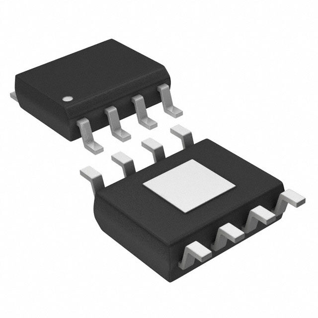
| 描述 | TVS DIODE 14VWM 20VC WLCSPTVS二极管阵列 UNI 1CH 16V 28A |
| 产品分类 | |
| 品牌 | NXP Semiconductors |
| 产品手册 | |
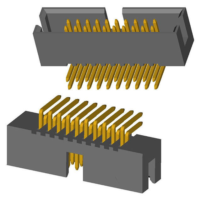
| 产品图片 |
|
| rohs | 符合RoHS无铅 / 符合限制有害物质指令(RoHS)规范要求 |
| 产品系列 | 二极管与整流器,TVS二极管,TVS二极管阵列,NXP Semiconductors IP4386CX4/P,315- |
| 数据手册 | |
| 产品型号 | IP4386CX4/P,315 |
| 不同频率时的电容 | 160pF @ 1MHz |
| 产品种类 | TVS二极管阵列 |
| 供应商器件封装 | 4-WLCSP(0.76x0.76) |
| 其它名称 | 568-7208-6 |
| 击穿电压 | 16 V |
| 功率-峰值脉冲 | - |
| 包装 | Digi-Reel® |
| 单向通道 | 1 |
| 双向通道 | - |
| 商标 | NXP Semiconductors |
| 安装类型 | 表面贴装 |
| 安装风格 | SMD/SMT |
| 封装 | Reel |
| 封装/外壳 | 4-WFBGA,WLCSP |
| 封装/箱体 | WLCSP-4 |
| 尺寸 | 0.76 mm W x 0.76 mm L x 0.61 mm H |
| 峰值浪涌电流 | 28 A |
| 峰值脉冲功率耗散 | 0.7 W |
| 工作温度 | -35°C ~ 85°C (TA) |
| 工作电压 | - 0.5 V to + 14 V |
| 工厂包装数量 | 9000 |
| 应用 | 通用 |
| 最大工作温度 | + 85 C |
| 最小工作温度 | - 30 C |
| 极性 | Unidirectional |
| 标准包装 | 1 |
| 电压-击穿(最小值) | 16V |
| 电压-反向关态(典型值) | 14V (最小值) |
| 电压-箝位(最大值)@Ipp | 20V |
| 电流-峰值脉冲(10/1000µs) | 28A (8/20µs) |
| 电源线路保护 | 无 |
| 端接类型 | SMD/SMT |
| 类型 | 齐纳 |
| 通道 | 1 Channel |
| 钳位电压 | 20 V |


- 商务部:美国ITC正式对集成电路等产品启动337调查
- 曝三星4nm工艺存在良率问题 高通将骁龙8 Gen1或转产台积电
- 太阳诱电将投资9.5亿元在常州建新厂生产MLCC 预计2023年完工
- 英特尔发布欧洲新工厂建设计划 深化IDM 2.0 战略
- 台积电先进制程称霸业界 有大客户加持明年业绩稳了
- 达到5530亿美元!SIA预计今年全球半导体销售额将创下新高
- 英特尔拟将自动驾驶子公司Mobileye上市 估值或超500亿美元
- 三星加码芯片和SET,合并消费电子和移动部门,撤换高东真等 CEO
- 三星电子宣布重大人事变动 还合并消费电子和移动部门
- 海关总署:前11个月进口集成电路产品价值2.52万亿元 增长14.8%


PDF Datasheet 数据手册内容提取
Important notice Dear Customer, On 7 February 2017 the former NXP Standard Product business became a new company with the tradename Nexperia. Nexperia is an industry leading supplier of Discrete, Logic and PowerMOS semiconductors with its focus on the automotive, industrial, computing, consumer and wearable application markets In data sheets and application notes which still contain NXP or Philips Semiconductors references, use the references to Nexperia, as shown below. Instead of http://www.nxp.com, http://www.philips.com/ or http://www.semiconductors.philips.com/, use http://www.nexperia.com Instead of sales.addresses@www.nxp.com or sales.addresses@www.semiconductors.philips.com, use salesaddresses@nexperia.com (email) Replace the copyright notice at the bottom of each page or elsewhere in the document, depending on the version, as shown below: - © NXP N.V. (year). All rights reserved or © Koninklijke Philips Electronics N.V. (year). All rights reserved Should be replaced with: - © Nexperia B.V. (year). All rights reserved. If you have any questions related to the data sheet, please contact our nearest sales office via e-mail or telephone (details via salesaddresses@nexperia.com). Thank you for your cooperation and understanding, Kind regards, Team Nexperia
IP4085CX4; IP4385CX4; (cid:2)(cid:3)(cid:4)(cid:5)(cid:6)(cid:7) IP4386CX4; IP4387CX4 Integrated high-performance ESD protection diodes Rev. 2 — 14 December 2012 Product data sheet 1. Product profile 1.1 General description Integrated high-performance protection diodes protecting appliances against ElectroStatic Discharge(ESD) of 30 kV, far exceeding IEC61000-4-2 level4 standard, overvoltage and wrong polarity. Each device includes one high-level ESD protection diode in a 4-channel 0.4mm (IP438xCX4) or 0.5mm (IP4085CX4) pitch Wafer Level Chip-Size Package(WLCSP). The anode and the cathode of ESD protection diode are each connected to two solder balls. 1.2 Features and benefits Single integrated high-performance ESD protection diode Surge immunity according to IEC61000-4-5 (8/20 s) up to 60A (IP4085CX4) ESD protection of >30kV contact discharge, far exceeding IEC61000-4-2, level4 Small 22 solder ball WLCSP package with 0.4mm or 0.5mm pitch 1.3 Applications General-purpose ESD protection such as for charger interfaces in: Mobile handsets Portable devices Wireless data systems
IP4085/4385/4386/4387/CX4 NXP Semiconductors Integrated high-performance ESD protection diodes 2. Pinning information Table 1. Pinning Pin Description Simplified outline Graphic symbol A1 and A2 cathode bump A1 A1 A2 B1 and B2 anode index area 1 2 B1 B2 006aad220 A B 008aaa236 transparent top view, solder balls facing down 3. Ordering information Table 2. Ordering info rmation Type number Package Name Description Version IP4085CX4/LF/P WLCSP4 wafer level chip-size package: 4bumps(22)[1] IP4085CX4/LF/P IP4385CX4/LF wafer level chip-size package: 4bumps(22)[2] IP4385CX4/LF IP4386CX4/P IP4386CX4/P IP4387CX4/P IP4387CX4/P [1] Size: 0.910.910.65 mm [2] Size: 0.760.760.61 mm IP4085_4385_4386_4387_CX4 All information provided in this document is subject to legal disclaimers. © NXP B.V. 2012. All rights reserved. Product data sheet Rev. 2 — 14 December 2012 2 of 18
IP4085/4385/4386/4387/CX4 NXP Semiconductors Integrated high-performance ESD protection diodes 4. Limiting values Table 3. Limiting valu es In accordance with the Absolute Maximum Rating System (IEC 60134). Symbol Parameter Conditions Min Max Unit V reverse standoff voltage IP4085CX4; IP4386CX4 0.5 +14 V RWM IP4385CX4 0.5 +5.5 V IP4387CX4 0.5 +8.0 V V electrostatic discharge voltage all pins to ground ESD contact discharge [1] 30 +30 kV air discharge [1] 15 +15 kV IEC 61000-4-2, level4; all pins to ground contact discharge 8 +8 kV air discharge 15 +15 kV I peak pulse current IEC 61000-4-5; t =8/20 s PP p IP4085CX4 60 - A IP4385CX4; IP4387CX4 33 - A IP4386CX4 28 - A I non-repetitive peak forward 10 pulses; 1 pulse per FSM current second IP4085CX4; IP4386CX4; 10 - A t =2ms p IP4085CX4; IP4386CX4; 8.5 - A t =5ms p IP4085CX4; IP4386CX4; 3.5 - A t =100ms p IP4385CX4; IP4387CX4; 11 - A t =2ms p IP4385CX4; IP4387CX4; 9 - A t =5ms p IP4385CX4; IP4387CX4; 5 - A t =100ms p P total power dissipation forward conducting [2] tot IP4085CX4 [3] - 1 W IP4385CX4; IP4386CX4; [3] - 0.7 W IP4387CX4 T storage temperature 55 +150 C stg T peak reflow temperature t 10 s - 260 C reflow(peak) p T ambient temperature 30 +85 C amb [1] Device tested with over 1000 pulses of 30kV contact discharges, according to the IEC61000-4-2 model. [2] Severe self-heating demands a heat-dissipation optimized Printed-Circuit Board (PCB) to prevent the device from de-soldering. For ambient temperature above 50 C, the guaranteed life time is 48 hours at 0.7 W, assuming Rth to be 130K/W as specified in Table4. [3] Permanent operation at maximum power dissipation and above maximum junction temperature will result in a reduced life time. IP4085_4385_4386_4387_CX4 All information provided in this document is subject to legal disclaimers. © NXP B.V. 2012. All rights reserved. Product data sheet Rev. 2 — 14 December 2012 3 of 18
IP4085/4385/4386/4387/CX4 NXP Semiconductors Integrated high-performance ESD protection diodes 5. Thermal characteristics Table 4. Thermal characteristics Symbol Parameter Conditions Typ Unit R thermal resistance from junction on a 2-layer PCB [1] 130 K/W th(j-a) to ambient [1] Depends on details of PCB layout. 6. Characteristics Table 5. Electrical ch aracteristics T = 25 C; unless otherwise specified. amb Symbol Parameter Conditions Min Typ Max Unit V breakdown voltage I = 15 mA BR R IP4085CX4; IP4386CX4 16 - - V IP4385CX4 7.0 - - V IP4387CX4 10 - - V V clamping voltage I =1A; T 85C at surge peak CL R amb pulse, according to IEC 61000-4-5 IP4085CX4 - - 20 V IP4385CX4 - - 10 V IP4386CX4 - - 20 V IP4387CX4 - - 13 V I reverse leakage current RM IP4085CX4; IP4385CX4 - - 200 nA V =+5V R IP4386CX4; V =+14V - - 200 nA R IP4387CX4; V =+8V - - 800 nA R C diode capacitance V =0 V; f=1 MHz d R IP4085CX4 - 180 - pF IP4385CX4 - 450 - pF IP4386CX4 - 160 - pF IP4387CX4 - 290 - pF V forward voltage I =850mA F F IP4085CX4 [1] - - 1.15 V [2] - - 1.3 V IP4385CX4 [1] - - 1.0 V [2] - - 1.1 V IP4386CX4 [1] - - 1.15 V [2] - - 1.3 V IP4387CX4 [1] - - 1.10 V [2] - - 1.25 V [1] Tamb +25 C [2] 30 C Tamb +85 C IP4085_4385_4386_4387_CX4 All information provided in this document is subject to legal disclaimers. © NXP B.V. 2012. All rights reserved. Product data sheet Rev. 2 — 14 December 2012 4 of 18
IP4085/4385/4386/4387/CX4 NXP Semiconductors Integrated high-performance ESD protection diodes 7. Application information 7.1 Forward current DC clamping voltage The forward current DC clamping voltage is an indicator of protection level of circuit from voltage sources with the wrong polarity. Figure1 shows basic measurement setup. IF VCL V 006aad221 Fig 1. Measuring DC clamping voltage with forward current 001aaj241 001aaj242 1.1 1.1 VCL VCL (V) (V) (1) 1.0 1.0 (1) (2) (2) 0.9 (3) 0.9 (3) 0.8 0.8 0.7 0.7 0 0.2 0.4 0.6 0.8 1.0 0 0.2 0.4 0.6 0.8 1.0 IF (A) IF (A) (1) Tamb = +25C (1) Tamb = +25C (2) Tamb = +85 C (2) Tamb = +85 C (3) Tamb = 30 C (3) Tamb = 30 C Fig 2. IP4085CX4: DC clamping voltage as a function Fig 3. IP4385CX4: DC clamping voltage as a function of forward current of forward current IP4085_4385_4386_4387_CX4 All information provided in this document is subject to legal disclaimers. © NXP B.V. 2012. All rights reserved. Product data sheet Rev. 2 — 14 December 2012 5 of 18
IP4085/4385/4386/4387/CX4 NXP Semiconductors Integrated high-performance ESD protection diodes 001aaj243 001aaj244 1.1 1.1 VCL VCL (V) (1) (V) 1.0 1.0 (1) (2) (3) (2) 0.9 0.9 (3) 0.8 0.8 0.7 0.7 0 0.2 0.4 0.6 0.8 1.0 0 0.2 0.4 0.6 0.8 1.0 IF (A) IF (A) (1) Tamb = +25C (1) Tamb = +25C (2) Tamb = +85 C (2) Tamb = +85 C (3) Tamb = 30 C (3) Tamb = 30 C Fig 4. IP4386CX4: DC clamping voltage as a function Fig 5. IP4387CX4: DC clamping voltage as a function of forward current of forward current IP4085_4385_4386_4387_CX4 All information provided in this document is subject to legal disclaimers. © NXP B.V. 2012. All rights reserved. Product data sheet Rev. 2 — 14 December 2012 6 of 18
IP4085/4385/4386/4387/CX4 NXP Semiconductors Integrated high-performance ESD protection diodes 7.2 Peak clamping voltage The peak clamping voltage for forward and reverse current pulses of 8/20s (IEC61000-4-5) is an indicator of protection level of circuits from power surges due to voltage discharges. The current pulse shape over time is shown in Figure7. The basic measurement setup for forward current and reverse current pulses respectively are shown in Figure6 and Figure12. VCL V IPP 006aad227 Fig 6. Measuring peak clamping voltage with forward current 001aaj558 120 IPP 100 % IPP; 8 μs (%) 80 e−t 50 % IPP; 20 μs 40 0 0 10 20 30 40 t (μs) Fig 7. 8/20 s current pulse waveform according to IEC 61000-4-5 IP4085_4385_4386_4387_CX4 All information provided in this document is subject to legal disclaimers. © NXP B.V. 2012. All rights reserved. Product data sheet Rev. 2 — 14 December 2012 7 of 18
IP4085/4385/4386/4387/CX4 NXP Semiconductors Integrated high-performance ESD protection diodes 006aad222 006aad223 17 20 VCL (V) VCL 15 (V) (3) (1) 16 13 (3) 11 (2) 12 9 (1) (2) 7 8 20 28 36 44 20 28 36 44 IF (A) IF (A) (1) Tamb = +25C (1) Tamb = +25C (2) Tamb = +85 C (2) Tamb = +85 C (3) Tamb = 30 C (3) Tamb = 30 C Fig 8. IP4085CX4:peak clamping voltage as a Fig 9. IP4385CX4: peak clamping voltage as a function of forward current function of forward current 006aad224 006aad225 20 20 (3) (2) VCL (1) VCL (V) (V) 16 16 12 12 (2) (3) (1) 8 8 20 28 36 44 20 28 36 44 IF (A) IF (A) (1) Tamb = +25C (1) Tamb = +25C (2) Tamb = +85 C (2) Tamb = +85 C (3) Tamb = 30 C (3) Tamb = 30 C Fig 10. IP4386CX4: peak clamping voltage as a Fig 11. IP4387CX4: peak clamping voltage as a function of forward current function of forward current IP4085_4385_4386_4387_CX4 All information provided in this document is subject to legal disclaimers. © NXP B.V. 2012. All rights reserved. Product data sheet Rev. 2 — 14 December 2012 8 of 18
IP4085/4385/4386/4387/CX4 NXP Semiconductors Integrated high-performance ESD protection diodes VCL V IPP 006aad226 Fig 12. Measuring peak clamping voltage with reverse current 006aad228 006aad229 19 8.75 VCL VCL (2) (V) (V) 8.50 (2) 18 8.25 (1) (1) 8.00 (3) 17 (3) 7.75 16 7.50 0.2 0.4 0.6 0.8 1.0 1.2 1.4 1.6 0.4 0.8 1.2 1.6 IR (A) IR (A) (1) Tamb = +25C (1) Tamb = +25C (2) Tamb = +85 C (2) Tamb = +85 C (3) Tamb = 30 C (3) Tamb = 30 C Fig 13. IP4085CX4: peak clamping voltage as a Fig 14. IP4385CX4: peak clamping voltage as a function of reverse current function of reverse current IP4085_4385_4386_4387_CX4 All information provided in this document is subject to legal disclaimers. © NXP B.V. 2012. All rights reserved. Product data sheet Rev. 2 — 14 December 2012 9 of 18
IP4085/4385/4386/4387/CX4 NXP Semiconductors Integrated high-performance ESD protection diodes 006aad230 006aad231 19 12.2 (2) VCL VCL (V) (2) (V) 18 11.8 (1) (1) 17 11.4 (3) (3) 16 11.0 0.3 0.7 1.1 1.5 0.4 0.8 1.2 1.6 IR (A) IR (A) (1) Tamb = +25C. (1) Tamb = +25C. (2) Tamb = +85 C. (2) Tamb = +85 C. (3) Tamb = 30 C. (3) Tamb = 30 C. Fig 15. IP4386CX4: peak clamping voltage as a Fig 16. IP4387CX4: peak clamping voltage as a function of reverse current function of reverse current Measurements are done on a heat-dissipation optimized PCB with massive copper area under the Device Under Test(DUT). IP4085_4385_4386_4387_CX4 All information provided in this document is subject to legal disclaimers. © NXP B.V. 2012. All rights reserved. Product data sheet Rev. 2 — 14 December 2012 10 of 18
IP4085/4385/4386/4387/CX4 NXP Semiconductors Integrated high-performance ESD protection diodes 8. Package outline WLCSP4: wafer level chip-size package; 4 bumps (2 x 2) D bump A1 index area A2 E A A1 detail X e b B e A 1 2 X European projection wlcsp4_2x2_po Fig 17. Package outline WLCSP4 Table 6. Package out line dimensions of IP4085CX4 (WLCSP4) Symbol Min Typ Max Unit A 0.60 0.65 0.70 mm A 0.22 0.24 0.26 mm 1 A 0.38 0.41 0.44 mm 2 b 0.27 0.32 0.37 mm D 0.86 0.91 0.96 mm E 0.86 0.91 0.96 mm e 0.5 0.5 0.5 mm IP4085_4385_4386_4387_CX4 All information provided in this document is subject to legal disclaimers. © NXP B.V. 2012. All rights reserved. Product data sheet Rev. 2 — 14 December 2012 11 of 18
IP4085/4385/4386/4387/CX4 NXP Semiconductors Integrated high-performance ESD protection diodes Table 7. Package out line dimensions of IP438xCX4 (WLCSP4) Symbol Min Typ Max Unit A 0.56 0.61 0.66 mm A 0.18 0.20 0.22 mm 1 A 0.38 0.41 0.44 mm 2 b 0.21 0.26 0.31 mm D 0.71 0.76 0.76 mm E 0.71 0.76 0.81 mm e 0.4 0.4 0.4 mm 9. Design and assembly recommendations 9.1 PCB design guidelines For optimum performance, use a Non-Solder Mask Defined (NSMD), also known as a copper-defined design, incorporating laser-drilled micro-vias connecting the ground pads to a buried ground-plane layer. This results in the lowest possible ground inductance and provides the best high frequency and ESD performance. Refer to Table8 for the recommended PCB design parameters. Table 8. Recommended PCB design parameters Parameter Value or Specification PCB pad diameter 200 m Micro-via diameter 100 m (0.004 inch) Solder mask aperture diameter 370 m Copper thickness 20 m to 40 m Copper finish AuNi PCB material FR4 9.2 PCB assembly guidelines for Pb-free soldering Table 9. Assembly recommendations Parameter Value or Specification Solder screen aperture diameter 330 m Solder screen thickness 100 m (0.004 inch) Solder paste: Pb-free SnAg (3% to 4%) Cu (0.5 % to 0.9%) Solder to flux ratio 50:50 Solder reflow profile see Figure18 IP4085_4385_4386_4387_CX4 All information provided in this document is subject to legal disclaimers. © NXP B.V. 2012. All rights reserved. Product data sheet Rev. 2 — 14 December 2012 12 of 18
IP4085/4385/4386/4387/CX4 NXP Semiconductors Integrated high-performance ESD protection diodes T (°C) Treflow(peak) 250 230 cooling rate 217 preheat t (s) t1 t2 t3 t4 t5 001aai943 The device is capable of withstanding at least three reflows of this profile. Fig 18. Pb-free solder reflow profile T able 10. Reflow soldering process characteristics Symbol Parameter Conditions Min Typ Max Unit T peak reflow temperature 230 - 260 C reflow(peak) t time 1 soak time 60 - 180 s 1 t time 2 time during T 250C - - 30 s 2 t time 3 time during T 230C 10 - 50 s 3 t time 4 time during T> 217C 30 - 150 s 4 t time 5 - - 540 s 5 dT/dt rate of change of cooling rate - - 6 C/s temperature pre-heat 2.5 - 4.0 C/s IP4085_4385_4386_4387_CX4 All information provided in this document is subject to legal disclaimers. © NXP B.V. 2012. All rights reserved. Product data sheet Rev. 2 — 14 December 2012 13 of 18
IP4085/4385/4386/4387/CX4 NXP Semiconductors Integrated high-performance ESD protection diodes 10. Soldering D e c (4×) e E solder resist solder paste = solderland f occupied area (4×) Dimensions in mm wlcsp4_2x2_fr Fig 19. Reflow soldering footprint WLCSP4 Table 11. Soldering dim ensions of IP4085CX4 (WLCSP4) Symbol Min Typ Max Unit c - 0.31 - mm D 0.86 0.91 0.96 mm E 0.86 0.91 0.96 mm e - 0.5 - mm f - 0.385 - mm Table 12. Soldering dim ensions of IP438xCX4 (WLCSP4) Symbol Min Typ Max Unit c - 0.25 - mm D 0.71 0.76 0.81 mm E 0.71 0.76 0.81 mm e - 0.4 - mm f - 0.325 - mm IP4085_4385_4386_4387_CX4 All information provided in this document is subject to legal disclaimers. © NXP B.V. 2012. All rights reserved. Product data sheet Rev. 2 — 14 December 2012 14 of 18
IP4085/4385/4386/4387/CX4 NXP Semiconductors Integrated high-performance ESD protection diodes 11. Revision history Table 13. Revision history Document ID Release Data sheet status Change Supersedes date notice IP4085_4385_4386_4387_CX4 v.2 20121214 Product data sheet - IP4085_4385_4386_4387_CX4 v.1 Modifications: • Basic type IP4085CX4/LF removed • Section 1 “Product profile”: updated • Section 2 “Pinning information”: updated • Functional diagram: removed • Table 3 “Limiting values”: updated • Table 5 “Electrical characteristics”. updated • Section 7 “Application information”. updated • Figure1, 6, 8 to 16: updated • Marking: removed • Section 8 “Package outline”: updated • Section 10 “Soldering”: added • Section 12 “Legal information”: updated IP4085_4385_4386_4387_CX4 v.1 20090326 Product data sheet - - IP4085_4385_4386_4387_CX4 All information provided in this document is subject to legal disclaimers. © NXP B.V. 2012. All rights reserved. Product data sheet Rev. 2 — 14 December 2012 15 of 18
IP4085/4385/4386/4387/CX4 NXP Semiconductors Integrated high-performance ESD protection diodes 12. Legal information 12.1 Data sheet status Document status[1][2] Product status[3] Definition Objective [short] data sheet Development This document contains data from the objective specification for product development. Preliminary [short] data sheet Qualification This document contains data from the preliminary specification. Product [short] data sheet Production This document contains the product specification. [1] Please consult the most recently issued document before initiating or completing a design. [2] The term ‘short data sheet’ is explained in section “Definitions”. [3] The product status of device(s) described in this document may have changed since this document was published and may differ in case of multiple devices. The latest product status information is available on the Internet at URLhttp://www.nxp.com. 12.2 Definitions Suitability for use — NXP Semiconductors products are not designed, authorized or warranted to be suitable for use in life support, life-critical or safety-critical systems or equipment, nor in applications where failure or Draft — The document is a draft version only. The content is still under malfunction of an NXP Semiconductors product can reasonably be expected internal review and subject to formal approval, which may result in to result in personal injury, death or severe property or environmental modifications or additions. NXP Semiconductors does not give any damage. NXP Semiconductors and its suppliers accept no liability for representations or warranties as to the accuracy or completeness of inclusion and/or use of NXP Semiconductors products in such equipment or information included herein and shall have no liability for the consequences of applications and therefore such inclusion and/or use is at the customer’s own use of such information. risk. Short data sheet — A short data sheet is an extract from a full data sheet Applications — Applications that are described herein for any of these with the same product type number(s) and title. A short data sheet is intended products are for illustrative purposes only. NXP Semiconductors makes no for quick reference only and should not be relied upon to contain detailed and representation or warranty that such applications will be suitable for the full information. For detailed and full information see the relevant full data specified use without further testing or modification. sheet, which is available on request via the local NXP Semiconductors sales office. In case of any inconsistency or conflict with the short data sheet, the Customers are responsible for the design and operation of their applications full data sheet shall prevail. and products using NXP Semiconductors products, and NXP Semiconductors accepts no liability for any assistance with applications or customer product Product specification — The information and data provided in a Product design. It is customer’s sole responsibility to determine whether the NXP data sheet shall define the specification of the product as agreed between Semiconductors product is suitable and fit for the customer’s applications and NXP Semiconductors and its customer, unless NXP Semiconductors and products planned, as well as for the planned application and use of customer have explicitly agreed otherwise in writing. In no event however, customer’s third party customer(s). Customers should provide appropriate shall an agreement be valid in which the NXP Semiconductors product is design and operating safeguards to minimize the risks associated with their deemed to offer functions and qualities beyond those described in the applications and products. Product data sheet. NXP Semiconductors does not accept any liability related to any default, damage, costs or problem which is based on any weakness or default in the 12.3 Disclaimers customer’s applications or products, or the application or use by customer’s third party customer(s). Customer is responsible for doing all necessary testing for the customer’s applications and products using NXP Limited warranty and liability — Information in this document is believed to Semiconductors products in order to avoid a default of the applications and be accurate and reliable. However, NXP Semiconductors does not give any the products or of the application or use by customer’s third party representations or warranties, expressed or implied, as to the accuracy or customer(s). NXP does not accept any liability in this respect. completeness of such information and shall have no liability for the consequences of use of such information. NXP Semiconductors takes no Limiting values — Stress above one or more limiting values (as defined in responsibility for the content in this document if provided by an information the Absolute Maximum Ratings System of IEC60134) will cause permanent source outside of NXP Semiconductors. damage to the device. Limiting values are stress ratings only and (proper) operation of the device at these or any other conditions above those given in In no event shall NXP Semiconductors be liable for any indirect, incidental, the Recommended operating conditions section (if present) or the punitive, special or consequential damages (including - without limitation - lost Characteristics sections of this document is not warranted. Constant or profits, lost savings, business interruption, costs related to the removal or repeated exposure to limiting values will permanently and irreversibly affect replacement of any products or rework charges) whether or not such the quality and reliability of the device. damages are based on tort (including negligence), warranty, breach of contract or any other legal theory. Terms and conditions of commercial sale — NXP Semiconductors products are sold subject to the general terms and conditions of commercial Notwithstanding any damages that customer might incur for any reason whatsoever, NXP Semiconductors’ aggregate and cumulative liability towards sale, as published at http://www.nxp.com/profile/terms, unless otherwise customer for the products described herein shall be limited in accordance agreed in a valid written individual agreement. In case an individual with the Terms and conditions of commercial sale of NXP Semiconductors. agreement is concluded only the terms and conditions of the respective agreement shall apply. NXP Semiconductors hereby expressly objects to Right to make changes — NXP Semiconductors reserves the right to make applying the customer’s general terms and conditions with regard to the changes to information published in this document, including without purchase of NXP Semiconductors products by customer. limitation specifications and product descriptions, at any time and without notice. This document supersedes and replaces all information supplied prior No offer to sell or license — Nothing in this document may be interpreted or to the publication hereof. construed as an offer to sell products that is open for acceptance or the grant, conveyance or implication of any license under any copyrights, patents or other industrial or intellectual property rights. IP4085_4385_4386_4387_CX4 All information provided in this document is subject to legal disclaimers. © NXP B.V. 2012. All rights reserved. Product data sheet Rev. 2 — 14 December 2012 16 of 18
IP4085/4385/4386/4387/CX4 NXP Semiconductors Integrated high-performance ESD protection diodes Export control — This document as well as the item(s) described herein In the event that customer uses the product for design-in and use in may be subject to export control regulations. Export might require a prior automotive applications to automotive specifications and standards, customer authorization from competent authorities. (a) shall use the product without NXP Semiconductors’ warranty of the product for such automotive applications, use and specifications, and (b) Quick reference data — The Quick reference data is an extract of the whenever customer uses the product for automotive applications beyond product data given in the Limiting values and Characteristics sections of this NXP Semiconductors’ specifications such use shall be solely at customer’s document, and as such is not complete, exhaustive or legally binding. own risk, and (c) customer fully indemnifies NXP Semiconductors for any Non-automotive qualified products — Unless this data sheet expressly liability, damages or failed product claims resulting from customer design and states that this specific NXP Semiconductors product is automotive qualified, use of the product for automotive applications beyond NXP Semiconductors’ the product is not suitable for automotive use. It is neither qualified nor tested standard warranty and NXP Semiconductors’ product specifications. in accordance with automotive testing or application requirements. NXP Semiconductors accepts no liability for inclusion and/or use of non-automotive qualified products in automotive equipment or applications. 12.4 Trademarks Notice: All referenced brands, product names, service names and trademarks are the property of their respective owners. 13. Contact information For more information, please visit: http://www.nxp.com For sales office addresses, please send an email to: salesaddresses@nxp.com IP4085_4385_4386_4387_CX4 All information provided in this document is subject to legal disclaimers. © NXP B.V. 2012. All rights reserved. Product data sheet Rev. 2 — 14 December 2012 17 of 18
IP4085/4385/4386/4387/CX4 NXP Semiconductors Integrated high-performance ESD protection diodes 14. Contents 1 Product profile. . . . . . . . . . . . . . . . . . . . . . . . . . 1 1.1 General description . . . . . . . . . . . . . . . . . . . . . 1 1.2 Features and benefits. . . . . . . . . . . . . . . . . . . . 1 1.3 Applications . . . . . . . . . . . . . . . . . . . . . . . . . . . 1 2 Pinning information. . . . . . . . . . . . . . . . . . . . . . 2 3 Ordering information. . . . . . . . . . . . . . . . . . . . . 2 4 Limiting values. . . . . . . . . . . . . . . . . . . . . . . . . . 3 5 Thermal characteristics . . . . . . . . . . . . . . . . . . 4 6 Characteristics. . . . . . . . . . . . . . . . . . . . . . . . . . 4 7 Application information. . . . . . . . . . . . . . . . . . . 5 7.1 Forward current DC clamping voltage . . . . . . . 5 7.2 Peak clamping voltage . . . . . . . . . . . . . . . . . . . 7 8 Package outline. . . . . . . . . . . . . . . . . . . . . . . . 11 9 Design and assembly recommendations . . . 12 9.1 PCB design guidelines. . . . . . . . . . . . . . . . . . 12 9.2 PCB assembly guidelines for Pb-free soldering. . . . . . . . . . . . . . . . . . . . . . . . . . . . . 12 10 Soldering . . . . . . . . . . . . . . . . . . . . . . . . . . . . . 14 11 Revision history. . . . . . . . . . . . . . . . . . . . . . . . 15 12 Legal information. . . . . . . . . . . . . . . . . . . . . . . 16 12.1 Data sheet status . . . . . . . . . . . . . . . . . . . . . . 16 12.2 Definitions. . . . . . . . . . . . . . . . . . . . . . . . . . . . 16 12.3 Disclaimers. . . . . . . . . . . . . . . . . . . . . . . . . . . 16 12.4 Trademarks. . . . . . . . . . . . . . . . . . . . . . . . . . . 17 13 Contact information. . . . . . . . . . . . . . . . . . . . . 17 14 Contents. . . . . . . . . . . . . . . . . . . . . . . . . . . . . . 18 Please be aware that important notices concerning this document and the product(s) described herein, have been included in section ‘Legal information’. © NXP B.V. 2012. All rights reserved. For more information, please visit: http://www.nxp.com For sales office addresses, please send an email to: salesaddresses@nxp.com Date of release: 14 December 2012 Document identifier: IP4085_4385_4386_4387_CX4