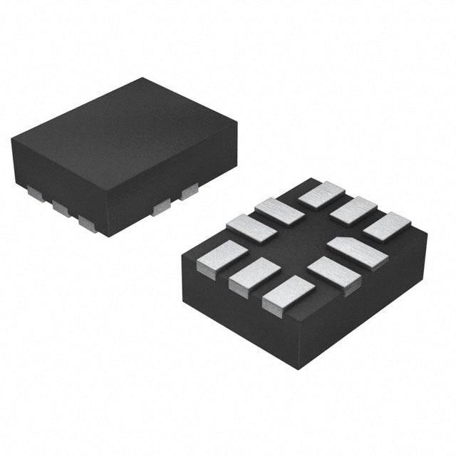
ICGOO在线商城 > INA210AIRSWT
- 型号: INA210AIRSWT
- 制造商: Texas Instruments
- 库位|库存: xxxx|xxxx
- 要求:
| 数量阶梯 | 香港交货 | 国内含税 |
| +xxxx | $xxxx | ¥xxxx |
查看当月历史价格
查看今年历史价格
INA210AIRSWT产品简介:
ICGOO电子元器件商城为您提供INA210AIRSWT由Texas Instruments设计生产,在icgoo商城现货销售,并且可以通过原厂、代理商等渠道进行代购。 提供INA210AIRSWT价格参考¥3.88-¥8.74以及Texas InstrumentsINA210AIRSWT封装/规格参数等产品信息。 你可以下载INA210AIRSWT参考资料、Datasheet数据手册功能说明书, 资料中有INA210AIRSWT详细功能的应用电路图电压和使用方法及教程。
| 参数 | 数值 |
| 产品目录 | 集成电路 (IC)半导体 |
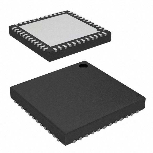
| 描述 | IC CURRENT MONITOR 1% 10UQFN电流灵敏放大器 Bi-Dir 0-Drift Ser Crnt Shunt Mon |
| DevelopmentKit | INA210-214EVM |
| 产品分类 | |
| 品牌 | Texas Instruments |
| 产品手册 | http://www.ti.com/litv/sbos437f |
| 产品图片 |
|
| rohs | 符合RoHS无铅 / 符合限制有害物质指令(RoHS)规范要求 |
| 产品系列 | 放大器 IC,电流灵敏放大器,Texas Instruments INA210AIRSWT- |
| 数据手册 | |
| 产品型号 | INA210AIRSWT |
| PCN设计/规格 | |
| 产品目录页面 | |
| 产品种类 | 电流灵敏放大器 |
| 供应商器件封装 | 10-UQFN(1.8x1.4) |
| 其它名称 | 296-24616-1 |
| 制造商产品页 | http://www.ti.com/general/docs/suppproductinfo.tsp?distId=10&orderablePartNumber=INA210AIRSWT |
| 功能 | 电流监控器 |
| 包装 | 剪切带 (CT) |
| 单位重量 | 6.100 mg |
| 商标 | Texas Instruments |
| 安装类型 | 表面贴装 |
| 安装风格 | SMD/SMT |
| 封装 | Reel |
| 封装/外壳 | 10-UFQFN |
| 封装/箱体 | UQFN-10 |
| 工作温度 | -40°C ~ 125°C |
| 工厂包装数量 | 250 |
| 感应方法 | 高/低端 |
| 拓扑结构 | Current Shunt Feedback |
| 标准包装 | 1 |
| 电压-输入 | 2.7 V ~ 26 V |
| 电流-输出 | - |
| 电源电压-最大 | 26 V |
| 电源电压-最小 | 2.7 V |
| 精度 | ±1% |
| 系列 | INA210 |


- 商务部:美国ITC正式对集成电路等产品启动337调查
- 曝三星4nm工艺存在良率问题 高通将骁龙8 Gen1或转产台积电
- 太阳诱电将投资9.5亿元在常州建新厂生产MLCC 预计2023年完工
- 英特尔发布欧洲新工厂建设计划 深化IDM 2.0 战略
- 台积电先进制程称霸业界 有大客户加持明年业绩稳了
- 达到5530亿美元!SIA预计今年全球半导体销售额将创下新高
- 英特尔拟将自动驾驶子公司Mobileye上市 估值或超500亿美元
- 三星加码芯片和SET,合并消费电子和移动部门,撤换高东真等 CEO
- 三星电子宣布重大人事变动 还合并消费电子和移动部门
- 海关总署:前11个月进口集成电路产品价值2.52万亿元 增长14.8%


PDF Datasheet 数据手册内容提取
Product Order Technical Tools & Support & Folder Now Documents Software Community INA210,INA211,INA212,INA213,INA214,INA215 SBOS437J–MAY2008–REVISEDFEBRUARY2017 INA21x Voltage Output, Low- or High-Side Measurement, Bidirectional, Zero-Drift Series, Current-Shunt Monitors 1 Features 3 Description • WideCommon-ModeRange:–0.3Vto26V The INA21x are voltage-output, current-shunt 1 monitors (also called current-sense amplifiers) that • OffsetVoltage:±35μV(Maximum,INA210) are commonly used for overcurrent protection, (EnablesShuntDropsof10-mVFull-Scale) precision-current measurement for system • Accuracy: optimization, or in closed-loop feedback circuits. This – GainError(MaximumOverTemperature): series of devices can sense drops across shunts at common-mode voltages from –0.3 V to 26 V, – ±0.5%(VersionC) independent of the supply voltage. Six fixed gains are – ±1%(VersionsAandB) available:50V/V,75V/V,100V/V,200V/V,500V/V, – 0.5-µV/°COffsetDrift(Maximum) or 1000 V/V. The low offset of the zero-drift architecture enables current sensing with maximum – 10-ppm/°CGainDrift(Maximum) dropsacrosstheshuntaslowas10-mVfull-scale. • ChoiceofGains: These devices operate from a single 2.7-V to 26-V – INA210:200V/V power supply, drawing a maximum of 100 µA of – INA211:500V/V supply current. All versions are specified over the – INA212:1000V/V extended operating temperature range (–40°C to +125°C), and offered in SC70 and UQFN – INA213:50V/V packages. – INA214:100V/V – INA215:75V/V DeviceInformation(1) • QuiescentCurrent:100 μA(Maximum) PARTNUMBER PACKAGE BODYSIZE(NOM) • SC70andThinUQFNPackages:AllModels SC70(6) 2.00mm×1.25mm INA21x UQFN(10) 1.80mm×1.40mm 2 Applications (1) For all available packages, see the orderable addendum at theendofthedatasheet. • NotebookComputers • CellPhones • TelecomEquipment • PowerManagement • BatteryChargers SimplifiedSchematic R Reference Supply SHUNT Load Voltage REF INA21x OUT Output GND R1 R3 IN- 2.7 V to 26 V V+ IN+ PRODUCT GAIN R and R R and R 3 4 1 2 R2 R4 INA210 200 5 kW 1 MW CBYPASS SC70 INA211 500 2 kW 1 MW 0.01mF INA212 1000 1 kW 1 MW to INA213 50 20 kW 1 MW 0.1mF INA214 100 10 kW 1 MW INA215 75 13.3 kW 1 MW V = (I ´R ) Gain + V OUT LOAD SHUNT REF Copyright © 2017,Texas Instruments Incorporated 1 An IMPORTANT NOTICE at the end of this data sheet addresses availability, warranty, changes, use in safety-critical applications, intellectualpropertymattersandotherimportantdisclaimers.PRODUCTIONDATA.
INA210,INA211,INA212,INA213,INA214,INA215 SBOS437J–MAY2008–REVISEDFEBRUARY2017 www.ti.com Table of Contents 1 Features.................................................................. 1 8 ApplicationandImplementation........................ 22 2 Applications........................................................... 1 8.1 ApplicationInformation............................................22 3 Description............................................................. 1 8.2 TypicalApplications................................................22 4 RevisionHistory..................................................... 2 9 PowerSupplyRecommendations...................... 25 5 PinConfigurationsandFunctions....................... 5 10 Layout................................................................... 25 6 Specifications......................................................... 6 10.1 LayoutGuidelines.................................................25 6.1 AbsoluteMaximumRatings......................................6 10.2 LayoutExample....................................................26 6.2 ESDRatings..............................................................6 11 DeviceandDocumentationSupport................. 27 6.3 RecommendedOperatingConditions.......................6 11.1 DocumentationSupport........................................27 6.4 ThermalInformation..................................................7 11.2 RelatedLinks........................................................27 6.5 ElectricalCharacteristics...........................................8 11.3 ReceivingNotificationofDocumentationUpdates27 6.6 TypicalCharacteristics............................................10 11.4 CommunityResources..........................................27 7 DetailedDescription............................................ 14 11.5 Trademarks...........................................................27 7.1 Overview.................................................................14 11.6 ElectrostaticDischargeCaution............................27 7.2 FunctionalBlockDiagram.......................................14 11.7 Glossary................................................................27 7.3 FeatureDescription.................................................15 12 Mechanical,Packaging,andOrderable Information........................................................... 28 7.4 DeviceFunctionalModes........................................16 4 Revision History NOTE:Pagenumbersforpreviousrevisionsmaydifferfrompagenumbersinthecurrentversion. ChangesfromRevisionI(September2016)toRevisionJ Page • Added2017copyrighttofrontpagegraphic ......................................................................................................................... 1 • DeletedDeviceOptionstable ................................................................................................................................................ 5 • AddedCommon-modeanaloginputs(VersionsBandC)toAbsoluteMaximumRatingstable........................................... 6 • ChangedHBMESDvalue(VersionA)from4000to2000VinESDRatingstable ............................................................. 6 • ChangedformattingofThermalInformationtablenote.......................................................................................................... 7 • DeletedstaticliteraturenumberfromdocumentreferenceinRelatedDocumentationsection .......................................... 27 ChangesfromRevisionH(June2016)toRevisionI Page • Deletedallnotesregardingpreviewdevicesthroughoutdatasheet;alldevicesnowactive................................................. 1 ChangesfromRevisionG(July2014)toRevisionH Page • ChangedFeaturessection:deletedlastbullet,changedpackagesbullet ............................................................................ 1 • DeletedlastApplicationsbullet.............................................................................................................................................. 1 • ChangedDescriptionsection.................................................................................................................................................. 1 • ChangedDeviceInformationtable ........................................................................................................................................ 1 • MovedstoragetemperaturetoAbsoluteMaximumRatingstable ........................................................................................ 6 • ChangedESDRatingstable:changedtitle,changedformattocurrentstandards............................................................... 6 • DeletedbothMachineModelrowsfromESDRatingstable ................................................................................................. 6 • ChangedfirstsentencereferencingEquation1inInputFilteringsection:replacedseenwithmeasured.......................... 16 • ChangedsecondsentencereferencingEquation1inInputFilteringsection ..................................................................... 17 • CorrectedpunctuationandaddedclaritytofirstandsecondparagraphsinShuttingDowntheINA21xSeriessection....18 • ChangedimpressedtopresentinfourthparagraphofShuttingDowntheINA21xSeriessection..................................... 18 2 SubmitDocumentationFeedback Copyright©2008–2017,TexasInstrumentsIncorporated ProductFolderLinks:INA210 INA211 INA212 INA213 INA214 INA215
INA210,INA211,INA212,INA213,INA214,INA215 www.ti.com SBOS437J–MAY2008–REVISEDFEBRUARY2017 ChangesfromRevisionF(June2014)toRevisionG Page • ChangedSimplifiedSchematic:addedequationbelowgaintable......................................................................................... 1 • ChangedV HBMspecificationsforversionAinHandlingRatingstable......................................................................... 6 (ESD) ChangesfromRevisionE(June2013)toRevisionF Page • Changedformattomeetlatestdatasheetstandards;addedPinFunctions,RecommendedOperatingConditions, andThermalInformationtables,Overview,FunctionalBlockDiagram,ApplicationInformation,PowerSupply Recommendations,andLayoutsections,andmovedexistingsections................................................................................ 1 • AddedINA215todocument .................................................................................................................................................. 1 • AddedINA215sub-bullettofourthFeaturesbullet ............................................................................................................... 1 • AddedINA215tosimplifiedschematictable ......................................................................................................................... 1 • AddedThermalInformationtable........................................................................................................................................... 6 • AddedINA215toFigure7.................................................................................................................................................... 10 • AddedINA215toFigure15.................................................................................................................................................. 11 • AddedINA215toFigure25.................................................................................................................................................. 18 ChangesfromRevisionD(November2012)toRevisionE Page ChangesfromRevisionC(August2012)toRevisionD Page • ChangedFrequencyResponse,BandwidthparameterinElectricalCharacteristicstable.................................................... 6 ChangesfromRevisionB(June2009)toRevisionC Page • AddedsiliconversionBrowtoInput,Common-ModeInputRangeparameterinElectricalCharacteristicstable................6 • AddedsiliconversionBESDratingstoAbsMaxtable.......................................................................................................... 6 • CorrectedtypoinFigure9 ................................................................................................................................................... 10 • UpdatedFigure12 ............................................................................................................................................................... 10 • ChangedInputFilteringsection............................................................................................................................................ 16 • AddedImprovingTransientRobustnesssection.................................................................................................................. 21 ChangesfromRevisionA(June2008)toRevisionB Page • AddedRSWpackagetodevicephoto.................................................................................................................................... 1 • AddedUQFNpackagetoFeatureslist................................................................................................................................... 1 • Updatedfrontpagegraphic.................................................................................................................................................... 1 • AddedRSWpackagepinoutdrawing.................................................................................................................................... 5 • Addedfootnote3toElectricalCharacteristicstable............................................................................................................... 6 • AddedUQFNpackageinformationtoTemperatureRangesectionofElectricalCharacteristicstable................................. 6 • ChangedFigure2toreflectoperatingtemperaturerange................................................................................................... 10 • ChangedFigure4toreflectoperatingtemperaturerange................................................................................................... 10 • ChangedFigure6toreflectoperatingtemperaturerange................................................................................................... 10 • ChangedFigure13toreflectoperatingtemperaturerange................................................................................................. 11 • ChangedFigure14toreflectoperatingtemperaturerange................................................................................................. 11 • AddedRSWdescriptiontotheBasicConnectionssection.................................................................................................. 15 • Changed60μVto100μVinlastsentenceoftheSelectingRSsection............................................................................. 15 Copyright©2008–2017,TexasInstrumentsIncorporated SubmitDocumentationFeedback 3 ProductFolderLinks:INA210 INA211 INA212 INA213 INA214 INA215
INA210,INA211,INA212,INA213,INA214,INA215 SBOS437J–MAY2008–REVISEDFEBRUARY2017 www.ti.com ChangesfromOriginal(May2008)toRevisionA Page • DeletedfirstfootnoteofElectricalCharacteristicstable......................................................................................................... 6 • ChangedFigure7 ................................................................................................................................................................ 10 • ChangedFigure15 .............................................................................................................................................................. 11 4 SubmitDocumentationFeedback Copyright©2008–2017,TexasInstrumentsIncorporated ProductFolderLinks:INA210 INA211 INA212 INA213 INA214 INA215
INA210,INA211,INA212,INA213,INA214,INA215 www.ti.com SBOS437J–MAY2008–REVISEDFEBRUARY2017 5 Pin Configurations and Functions DCKPackage 6-PinSC70 RSWPackage TopView 10-PinThinUQFN TopView REF 1 6 OUT NC(1) V+ GND 2 5 IN- 7 6 REF 8 5 IN- V+ 3 4 IN+ GND 9 4 IN- OUT 10 3 IN+ 1 2 NC(1) IN+ (1) NC denotes no internal connection. These pinscanbeleftfloatingorconnectedtoany voltagebetweenV–andV+. PinFunctions PIN I/O DESCRIPTION NAME DCK RSW GND 2 9 Analog Ground Analog IN– 5 4,5 Connecttoloadsideofshuntresistor input Analog IN+ 4 2,3 Connecttosupplysideofshuntresistor input NC — 1,7 — Notinternallyconnected.Leavefloatingorconnecttoground. Analog OUT 6 10 Outputvoltage output Analog REF 1 8 Referencevoltage,0VtoV+ input V+ 3 6 Analog Powersupply,2.7Vto26V Copyright©2008–2017,TexasInstrumentsIncorporated SubmitDocumentationFeedback 5 ProductFolderLinks:INA210 INA211 INA212 INA213 INA214 INA215
INA210,INA211,INA212,INA213,INA214,INA215 SBOS437J–MAY2008–REVISEDFEBRUARY2017 www.ti.com 6 Specifications 6.1 Absolute Maximum Ratings overoperatingfree-airtemperaturerange(unlessotherwisenoted)(1) MIN MAX UNIT Supplyvoltage,V 26 V S Differential(V )–(V ) –26 26 V IN+ IN– Common-mode(VersionA)(3) GND–0.3 26 V Analoginputs,V ,V (2) IN+ IN– Common-mode(VersionB)(3) GND–0.1 26 V Common-mode(VersionC)(3) GND–0.1 26 V REFinput GND–0.3 (V )+0.3 V S Output(3) GND–0.3 (V )+0.3 V S Inputcurrentintoanyterminal(3) 5 mA Operatingtemperature –55 150 °C Junctiontemperature 150 °C Storagetemperature,T –65 150 °C stg (1) StressesbeyondthoselistedunderAbsoluteMaximumRatingsmaycausepermanentdamagetothedevice.Thesearestressratings only,whichdonotimplyfunctionaloperationofthedeviceattheseoranyotherconditionsbeyondthoseindicatedunderRecommended OperatingConditions.Exposuretoabsolute-maximum-ratedconditionsforextendedperiodsmayaffectdevicereliability. (2) V andV arethevoltagesattheIN+andIN–pins,respectively. IN+ IN– (3) Inputvoltageatanyterminalmayexceedthevoltageshownifthecurrentatthatpinislimitedto5mA. 6.2 ESD Ratings VALUE UNIT INA21x,(VERSIONA) Human-bodymodel(HBM),perANSI/ESDA/JEDECJS-001(1) ±2000 V Electrostaticdischarge V (ESD) Charged-devicemodel(CDM),perJEDECspecificationJESD22-C101(2) ±1000 INA21x,(VERSIONSBANDC) Human-bodymodel(HBM),perANSI/ESDA/JEDECJS-001(1) ±3500 V Electrostaticdischarge V (ESD) Charged-devicemodel(CDM),perJEDECspecificationJESD22-C101(2) ±1000 (1) JEDECdocumentJEP155statesthat500-VHBMallowssafemanufacturingwithastandardESDcontrolprocess. (2) JEDECdocumentJEP157statesthat250-VCDMallowssafemanufacturingwithastandardESDcontrolprocess. 6.3 Recommended Operating Conditions overoperatingfree-airtemperaturerange(unlessotherwisenoted) MIN NOM MAX UNIT V Common-modeinputvoltage 12 V CM V Operatingsupplyvoltage 5 V S T Operatingfree-airtemperature –40 125 °C A 6 SubmitDocumentationFeedback Copyright©2008–2017,TexasInstrumentsIncorporated ProductFolderLinks:INA210 INA211 INA212 INA213 INA214 INA215
INA210,INA211,INA212,INA213,INA214,INA215 www.ti.com SBOS437J–MAY2008–REVISEDFEBRUARY2017 6.4 Thermal Information INA21x THERMALMETRIC(1) DCK(SC70) RSW(UQFN) UNIT 6PINS 10PINS R Junction-to-ambientthermalresistance 227.3 107.3 °C/W θJA R Junction-to-case(top)thermalresistance 79.5 56.5 °C/W θJC(top) R Junction-to-boardthermalresistance 72.1 18.7 °C/W θJB ψ Junction-to-topcharacterizationparameter 3.6 1.1 °C/W JT ψ Junction-to-boardcharacterizationparameter 70.4 18.7 °C/W JB R Junction-to-case(bottom)thermalresistance N/A N/A °C/W θJC(bot) (1) Formoreinformationabouttraditionalandnewthermalmetrics,seetheSemiconductorandICPackageThermalMetricsapplication report. Copyright©2008–2017,TexasInstrumentsIncorporated SubmitDocumentationFeedback 7 ProductFolderLinks:INA210 INA211 INA212 INA213 INA214 INA215
INA210,INA211,INA212,INA213,INA214,INA215 SBOS437J–MAY2008–REVISEDFEBRUARY2017 www.ti.com 6.5 Electrical Characteristics atT =25°C,V =V –V A SENSE IN+ IN– INA210,INA213,INA214,andINA215:V =5V,V =12V,andV =V /2,unlessotherwisenoted S IN+ REF S INA211andINA212:V =12V,V =12V,andV =V /2,unlessotherwisenoted S IN+ REF S PARAMETER TESTCONDITIONS MIN TYP MAX UNIT INPUT VersionA –0.3 26 TA=–40°Cto+125°C VCM Common-modeinputrange V VersionsBandC –0.1 26 TA=–40°Cto+125°C INA210,INA211, INA212,INA214, VIN+=0Vto26VVSENSE=0mV 105 140 CMRR Common-mode INA215 TA=–40°Cto+125°C dB rejectionratio INA213 VIN+=0Vto26VVSENSE=0mV 100 120 TA=–40°Cto+125°C INA210,INA211, INA212 VSENSE=0mV ±0.55 ±35 VO Offsetvoltage,RTI(1) INA213 VSENSE=0mV ±5 ±100 µV INA214,INA215 VSENSE=0mV ±1 ±60 dVOS/dT RTIvstemperature VTASE=NS–E40=°0CmtoV+125°C 0.1 0.5 µV/°C VS=2.7Vto18V PSRR RTIvspowersupplyratio VIN+=18V ±0.1 ±10 µV/V VSENSE=0mV IIB Inputbiascurrent VSENSE=0mV 15 28 35 µA IIO Inputoffsetcurrent VSENSE=0mV ±0.02 µA OUTPUT INA210 200 INA211 500 INA212 1000 G Gain V/V INA213 50 INA214 100 INA215 75 VSENSE=–5mVto5mV TA=–40°Cto+125°C ±0.02% ±1% (VersionsAandB) EG Gainerror VSENSE=–5mVto5mV TA=–40°Cto+125°C ±0.02% ±0.5% (VersionC) Gainerrorvstemperature TA=–40°Cto+125°C 3 10 ppm/°C Nonlinearityerror VSENSE=–5mVto5mV ±0.01% Maximumcapacitiveload Nosustainedoscillation 1 nF VOLTAGEOUTPUT(2) SwingtoV+power-supplyrail RL=10kΩtoGND (V+)–0.05 (V+)–0.2 V TA=–40°Cto+125°C SwingtoGND RTAL==–1400k°ΩCttooG+1N2D5°C (VGND)+0.005 (VGND)+0.05 V FREQUENCYRESPONSE CLOAD=10pF,INA210 14 CLOAD=10pF,INA211 7 CLOAD=10pF,INA212 4 BW Bandwidth kHz CLOAD=10pF,INA213 80 CLOAD=10pF,INA214 30 CLOAD=10pF,INA215 40 SR Slewrate 0.4 V/µs NOISE,RTI(1) Voltagenoisedensity 25 nV/√Hz (1) RTI=referred-to-input. (2) SeeTypicalCharacteristiccurve,OutputVoltageSwingvsOutputCurrent(Figure10). 8 SubmitDocumentationFeedback Copyright©2008–2017,TexasInstrumentsIncorporated ProductFolderLinks:INA210 INA211 INA212 INA213 INA214 INA215
INA210,INA211,INA212,INA213,INA214,INA215 www.ti.com SBOS437J–MAY2008–REVISEDFEBRUARY2017 Electrical Characteristics (continued) atT =25°C,V =V –V A SENSE IN+ IN– INA210,INA213,INA214,andINA215:V =5V,V =12V,andV =V /2,unlessotherwisenoted S IN+ REF S INA211andINA212:V =12V,V =12V,andV =V /2,unlessotherwisenoted S IN+ REF S PARAMETER TESTCONDITIONS MIN TYP MAX UNIT POWERSUPPLY VS Operatingvoltagerange TA=–40°Cto+125°C 2.7 26 V IQ Quiescentcurrent VSENSE=0mV 65 100 µA IQovertemperature TA=–40°Cto+125°C 115 µA TEMPERATURERANGE Specifiedrange –40 125 °C Operatingrange –55 150 °C SC70 250 °C/W θJA Thermalresistance ThinUQFN 80 °C/W Copyright©2008–2017,TexasInstrumentsIncorporated SubmitDocumentationFeedback 9 ProductFolderLinks:INA210 INA211 INA212 INA213 INA214 INA215
INA210,INA211,INA212,INA213,INA214,INA215 SBOS437J–MAY2008–REVISEDFEBRUARY2017 www.ti.com 6.6 Typical Characteristics TheINA210isusedfortypicalcharacteristicsatT =25°C,V =5V,V =12V,andV =V /2,unlessotherwisenoted. A S IN+ REF S 100 80 60 V) 40 m on e ( 20 ati ag opul Volt 0 P et -20 s Off -40 -60 -80 5 0 5 0 5 0 5 0 5 0 5 0 5 0 5 -100 -3 -3 -2 -2 -1 -1 - 1 1 2 2 3 3 -50 -25 0 25 50 75 100 125 150 Offset Voltage (mV) Temperature (°C) Figure1.InputOffsetVoltageProductionDistribution Figure2.OffsetVoltagevsTemperature 5 4 3 2 pulation R (V/V)m 10 o R P M -1 C -2 -3 -4 050505050505050505050 -5 5.4.4.3.3.2.2.1.1.0. 0.1.1.2.2.3.3.4.4.5. -50 -25 0 25 50 75 100 125 150 ---------- Common-Mode Rejection Ratio (mV/V) Temperature (°C) Figure3.Common-ModeRejectionProductionDistribution Figure4.Common-ModeRejectionRatiovsTemperature 1.0 0.8 0.6 0.4 n %) atio or ( 0.2 pul Err 0 Po ain –0.2 G –0.4 –0.6 –0.8 -1.0-0.9-0.8-0.7-0.6-0.5-0.4-0.3-0.2-0.100.10.20.30.40.50.60.70.80.91.0 –1.0–50 –25 0 25 50 75 100 125 150 Gain Error (%) Temperature (°C) Figure5.GainErrorProductionDistribution Figure6.GainErrorvsTemperature 10 SubmitDocumentationFeedback Copyright©2008–2017,TexasInstrumentsIncorporated ProductFolderLinks:INA210 INA211 INA212 INA213 INA214 INA215
INA210,INA211,INA212,INA213,INA214,INA215 www.ti.com SBOS437J–MAY2008–REVISEDFEBRUARY2017 Typical Characteristics (continued) TheINA210isusedfortypicalcharacteristicsatT =25°C,V =5V,V =12V,andV =V /2,unlessotherwisenoted. A S IN+ REF S 70 160 INA210 INA211 60 INA212 INA213 B) 140 d 50 INA214 INA215 atio ( 120 R 40 n 100 ain (dB) 30 Rejectio 80 G 20 y 60 pl p 10 Su 40 er- 0 w 20 o P -10 0 10 100 1k 10k 100k 1M 10M 1 10 100 1k 10k 100k Frequency (Hz) Frequency (Hz) V =5V+250-mVsinedisturbance S V =0V V =2.5V V =shorted CM REF DIF Figure7.GainvsFrequency Figure8.Power-SupplyRejectionRatiovsFrequency 160 V+ Ratio (db) 114200 g (V) ((VV((++VV))++––))10––..1525 on 100 win (V+)–2.5 ecti e S (V+)–3 Mode Rej 8600 ut Voltag GNGDN D+ +2 .35 n- 40 utp GND + 2 mmo 20 O GNGDN D+ +1. 51 TTA== –2450CC Co GND + 0.5 TA= 125C 0 GND A 1 10 100 1k 10k 100k 1M 0 5 10 15 20 25 30 35 40 Frequency (Hz) Output Current (mA) VS=5V VCM=1Vsine VDIF=shorted VS=2.7V VS=2.7V VS=5Vto26V VREF=2.5V VS=2.7Vto26V Figure9.Common-ModeRejectionRatiovsFrequency Figure10.OutputVoltageSwingvsOutputCurrent 50 30 40 25 (µA)nput Bias Current 321000 put Bias Current (A)m 2110505 I n 0 I 0V 0 0V 2.5V 2.5V –10 -5 0 5 10 15 20 25 30 0 5 10 15 20 25 30 Common-Mode Voltage (V) Common-Mode Voltage (V) I ,I ,V =0V B+ B– REF I ,I , IB+,IB–,VREF=2.5V IB+,IB–,VREF=0V VREBF+=B2–.5V IB+,VREF=2.5V Figure11.InputBiasCurrentvsCommon-ModeVoltage Figure12.InputBiasCurrentvsCommon-ModeVoltage WithSupplyVoltage=5V WithSupplyVoltage=0V(Shutdown) Copyright©2008–2017,TexasInstrumentsIncorporated SubmitDocumentationFeedback 11 ProductFolderLinks:INA210 INA211 INA212 INA213 INA214 INA215
INA210,INA211,INA212,INA213,INA214,INA215 SBOS437J–MAY2008–REVISEDFEBRUARY2017 www.ti.com Typical Characteristics (continued) TheINA210isusedfortypicalcharacteristicsatT =25°C,V =5V,V =12V,andV =V /2,unlessotherwisenoted. A S IN+ REF S 35 100 90 30 80 (µA)s Current 221505 nt Current(μA) 765000 a e 40 nput Bi 10 Quiesc 30 I 20 5 10 0 0 –50 –25 0 25 50 75 100 125 150 –50 –25 0 25 50 75 100 125 150 Temperature (°C) Temperature (°C) Figure13.InputBiasCurrentvsTemperature Figure14.QuiescentCurrentvsTemperature 100 z) Ö nV/ v) ered Voltage Noise ( 10 Referred-to-Inputage Noise (200nV/di eff olt R V put- IINNAA221120 IINNAA221131 n I INA214 INA215 1 10 100 1k 10k 100k Time (1s/div) Frequency (Hz) VS=2.5V VCM=0V VDIF=0V VS=2.5V VREF=0V VIN–,VIN+=0V VREF=0V Figure15.Input-ReferredVoltageNoisevsFrequency Figure16.0.1-Hzto10-HzVoltageNoise(Referred-To-Input) e 2VPPOutput OutputVoltage Output Voltag(0.5V/diV) 10mVPPInput e Voltage (1V/div) 0V CommonVoltage Output Voltage od (4 M 0 nput Voltage(5mV/diV) Common- 0V mV/div) I Time (100ms/div) Time (50μs/div) Figure17.StepResponse(10-mV InputStep) Figure18.Common-ModeVoltageTransientResponse PP 12 SubmitDocumentationFeedback Copyright©2008–2017,TexasInstrumentsIncorporated ProductFolderLinks:INA210 INA211 INA212 INA213 INA214 INA215
INA210,INA211,INA212,INA213,INA214,INA215 www.ti.com SBOS437J–MAY2008–REVISEDFEBRUARY2017 Typical Characteristics (continued) TheINA210isusedfortypicalcharacteristicsatT =25°C,V =5V,V =12V,andV =V /2,unlessotherwisenoted. A S IN+ REF S InvertingInput NoninvertingInput Output Output v v di di V/ V/ 2 2 0V 0V Time (250μs/div) Time (250μs/div) V =5V V =12V V =2.5V V =5V V =12V V =2.5V S CM REF S CM REF Figure19.InvertingDifferentialInputOverload Figure20.NoninvertingDifferentialInputOverload SupplyVoltage SupplyVoltage OutputVoltage OutputVoltage V/div V/div 1 1 0V 0V Time (100μs/div) Time (100μs/div) 1-kHzstepwithV 1-kHzstepwith VS=5V =0V DIFF VREF=0V VS=5V VDIFF=0V VREF=2.5V Figure21.Start-UpResponse Figure22.BrownoutRecovery Copyright©2008–2017,TexasInstrumentsIncorporated SubmitDocumentationFeedback 13 ProductFolderLinks:INA210 INA211 INA212 INA213 INA214 INA215
INA210,INA211,INA212,INA213,INA214,INA215 SBOS437J–MAY2008–REVISEDFEBRUARY2017 www.ti.com 7 Detailed Description 7.1 Overview The INA21x are 26-V, common-mode, zero-drift topology, current-sensing amplifiers that can be used in both low-sideandhigh-sideconfigurations.Thesespecially-designed,current-sensingamplifiersareabletoaccurately measure voltages developed across current-sensing resistors on common-mode voltages that far exceed the supply voltage powering the device. Current can be measured on input voltage rails as high as 26 V while the devicecanbepoweredfromsupplyvoltagesaslowas2.7V. The zero-drift topology enables high-precision measurements with maximum input offset voltages as low as 35 µV with a maximum temperature contribution of 0.5 µV/°C over the full temperature range of –40°C to +125°C. 7.2 Functional Block Diagram V+ IN- - OUT IN+ + REF GND Copyright © 2017, Texas Instruments Incorporated 14 SubmitDocumentationFeedback Copyright©2008–2017,TexasInstrumentsIncorporated ProductFolderLinks:INA210 INA211 INA212 INA213 INA214 INA215
INA210,INA211,INA212,INA213,INA214,INA215 www.ti.com SBOS437J–MAY2008–REVISEDFEBRUARY2017 7.3 Feature Description 7.3.1 BasicConnections Figure 23 shows the basic connections of the INA21x. Connect the input pins (IN+ and IN–) as closely as possibletotheshuntresistortominimizeanyresistanceinserieswiththeshuntresistor. RSHUNT Power Supply Load 5-V Supply CBYPASS 0.1 µF V+ IN- - OUT ADC Microcontroller + IN+ REF GND Copyright © 2017, Texas Instruments Incorporated Figure23. TypicalApplication Power-supply bypass capacitors are required for stability. Applications with noisy or high-impedance power supplies may require additional decoupling capacitors to reject power-supply noise. Connect bypass capacitors closetothedevicepins. On the RSW package options, two pins are provided for each input. Tie these pins together (that is, tie IN+ to IN+andtieIN– toIN–). 7.3.2 SelectingR S The zero-drift offset performance of the INA21x offers several benefits. Most often, the primary advantage of the low offset characteristic enables lower full-scale drops across the shunt. For example, non-zero-drift current shuntmonitorstypicallyrequireafull-scalerangeof100mV. The INA21x series gives equivalent accuracy at a full-scale range on the order of 10 mV. This accuracy reduces shuntdissipationbyanorderofmagnitudewithmanyadditionalbenefits. Alternatively, there are applications that must measure current over a wide dynamic range that can take advantageofthelowoffsetonthelowendofthemeasurement.Mostoften,theseapplicationscanusethelower gains of the INA213, INA214, or INA215 to accommodate larger shunt drops on the upper end of the scale. For instance, an INA213 operating on a 3.3-V supply can easily handle a full-scale shunt drop of 60 mV, with only 100μVofoffset. Copyright©2008–2017,TexasInstrumentsIncorporated SubmitDocumentationFeedback 15 ProductFolderLinks:INA210 INA211 INA212 INA213 INA214 INA215
INA210,INA211,INA212,INA213,INA214,INA215 SBOS437J–MAY2008–REVISEDFEBRUARY2017 www.ti.com 7.4 Device Functional Modes 7.4.1 InputFiltering An obvious and straightforward filtering location is at the device output. However, this location negates the advantage of the low output impedance of the internal buffer. The only other filtering option is at the device input pins. This location, though, does require consideration of the ±30% tolerance of the internal resistances. Figure24showsafilterplacedattheinputspins. V+ V CM RS< 10W RINT V OUT R Bias SHUNT C F R < 10W S V REF R INT Load Figure24. FilteratInputPins The addition of external series resistance, however, creates an additional error in the measurement so the value of these series resistors must be kept to 10 Ω (or less, if possible) to reduce impact to accuracy. The internal bias network shown in Figure 24 present at the input pins creates a mismatch in input bias currents when a differential voltage is applied between the input pins. If additional external series filter resistors are added to the circuit, the mismatch in bias currents results in a mismatch of voltage drops across the filter resistors. This mismatch creates a differential error voltage that subtracts from the voltage developed at the shunt resistor. This error results in a voltage at the device input pins that is different than the voltage developed across the shunt resistor. Without the additional series resistance, the mismatch in input bias currents has little effect on device operation. The amount of error these external filter resistors add to the measurement can be calculated using Equation2wherethegainerrorfactoriscalculatedusingEquation1. The amount of variance in the differential voltage present at the device input relative to the voltage developed at the shunt resistor is based both on the external series resistance value as well as the internal input resistors, R3 and R4 (or R as shown in Figure 24). The reduction of the shunt voltage reaching the device input pins INT appears as a gain error when comparing the output voltage relative to the voltage across the shunt resistor. A factorcanbecalculatedtodeterminetheamountofgainerrorthatisintroducedbytheadditionofexternalseries resistance. The equation used to calculate the expected deviation from the shunt voltage to what is measured at thedeviceinputpinsisgiveninEquation1: (1250´R ) INT Gain Error Factor = (1250´R ) + (1250´R ) + (R ´R ) S INT S INT where: • R istheinternalinputresistor(R3andR4),and INT • R istheexternalseriesresistance. (1) S 16 SubmitDocumentationFeedback Copyright©2008–2017,TexasInstrumentsIncorporated ProductFolderLinks:INA210 INA211 INA212 INA213 INA214 INA215
INA210,INA211,INA212,INA213,INA214,INA215 www.ti.com SBOS437J–MAY2008–REVISEDFEBRUARY2017 Device Functional Modes (continued) With the adjustment factor from Equation 1, including the device internal input resistance, this factor varies with eachgainversion,asshowninTable1.EachindividualdevicegainerrorfactorisshowninTable2. Table1.InputResistance PRODUCT GAIN R (kΩ) INT INA210 200 5 INA211 500 2 INA212 1000 1 INA213 50 20 INA214 100 10 INA215 75 13.3 Table2.DeviceGainErrorFactor PRODUCT SIMPLIFIEDGAINERRORFACTOR 1000 INA210 R + 1000 S 10,000 INA211 (13´R )+ 10,000 S 5000 INA212 (9´R )+ 5000 S 20,000 INA213 (17´R )+ 20,000 S 10,000 INA214 (9´R )+ 10,000 S 8,000 INA215 (7 x RS) + 8,000 The gain error that can be expected from the addition of the external series resistors can then be calculated basedonEquation2: Gain Error (%) = 100-(100´Gain Error Factor) (2) For example, using an INA212 and the corresponding gain error equation from Table 2, a series resistance of 10 Ω results in a gain error factor of 0.982. The corresponding gain error is then calculated using Equation 2, resulting in a gain error of approximately 1.77% solely because of the external 10-Ω series resistors. Using an INA213 with the same 10-Ω series resistor results in a gain error factor of 0.991 and a gain error of 0.84% again solelybecauseoftheseexternalresistors. Copyright©2008–2017,TexasInstrumentsIncorporated SubmitDocumentationFeedback 17 ProductFolderLinks:INA210 INA211 INA212 INA213 INA214 INA215
INA210,INA211,INA212,INA213,INA214,INA215 SBOS437J–MAY2008–REVISEDFEBRUARY2017 www.ti.com 7.4.2 ShuttingDowntheINA21xSeries Although the INA21x series does not have a shutdown pin, the low power consumption of the device allows the output of a logic gate or transistor switch to power the INA21x. This gate or switch turns on and turns off the INA21xpower-supplyquiescentcurrent. However, in current shunt monitoring applications, there is also a concern for how much current is drained from the shunt circuit in shutdown conditions. Evaluating this current drain involves considering the simplified schematicoftheINA21xinshutdownmode,asshowninFigure25. R Supply SHUNT Load Reference Voltage REF INA21x OUT Output GND 1 MW R3 IN- Shutdown V+ IN+ Control PRODUCT R and R 1 MW R4 INA210 35 kW 4 C INA211 2 kW BYPASS INA212 1 kW INA213 20 kW INA214 10 kW INA215 13.3 kW Copyright © 2017,Texas Instruments Incorporated NOTE: 1-MΩpathsfromshuntinputstoreferenceandINA21xoutputs. Figure25. BasicCircuitforShuttingDownTheINA21xWithaGroundedReference Note that there is typically slightly more than 1-MΩ impedance (from the combination of 1-MΩ feedback and 5-kΩ input resistors) from each input of the INA21x to the OUT pin and to the REF pin. The amount of current flowing through these pins depends on the respective ultimate connection. For example, if the REF pin is grounded, the calculation of the effect of the 1-MΩ impedance from the shunt to ground is straightforward. However, if the reference or op amp is powered while the INA21x is shut down, the calculation is direct; instead of assuming 1 MΩ to ground, however, assume 1 MΩ to the reference voltage. If the reference or op amp is also shut down, some knowledge of the reference or op amp output impedance under shutdown conditions is required. For instance, if the reference source behaves as an open circuit when not powered, little or no current flowsthroughthe1-MΩpath. Regarding the 1-MΩ path to the output pin, the output stage of a disabled INA21x does constitute a good path to ground. Consequently, this current is directly proportional to a shunt common-mode voltage present across a 1- MΩ resistor. As a final note, when the device is powered up, there is an additional, nearly constant, and well-matched 25 μA that flows in each of the inputs as long as the shunt common-mode voltage is 3 V or higher. Below 2-V common- mode,theonlycurrenteffectsaretheresultofthe1-MΩ resistors. 18 SubmitDocumentationFeedback Copyright©2008–2017,TexasInstrumentsIncorporated ProductFolderLinks:INA210 INA211 INA212 INA213 INA214 INA215
INA210,INA211,INA212,INA213,INA214,INA215 www.ti.com SBOS437J–MAY2008–REVISEDFEBRUARY2017 7.4.3 REFInputImpedanceEffects As with any difference amplifier, the INA21x series common-mode rejection ratio is affected by any impedance present at the REF input. This concern is not a problem when the REF pin is connected directly to most references or power supplies. When using resistive dividers from the power supply or a reference voltage, the REFpinmustbebufferedbyanopamp. In systems where the INA21x output can be sensed differentially, such as by a differential input analog-to-digital converter (ADC) or by using two separate ADC inputs, the effects of external impedance on the REF input can be cancelled. Figure 26 depicts a method of taking the output from the INA21x by using the REF pin as a reference. Supply RSHUNT Load ADC Device REF OUT Output GND R1 R3 IN- 2.7 V to 26 V V+ IN+ R R 2 4 C BYPASS 0.01mF to 0.1mF Copyright © 2017,Texas Instruments Incorporated Figure26. SensingtheINA21xtoCanceltheEffectsofImpedanceontheREFInput 7.4.4 UsingTheINA21xWithCommon-ModeTransientsAbove26V With a small amount of additional circuitry, the INA21x series can be used in circuits subject to transients higher than 26 V, such as automotive applications. Use only zener diode or zener-type transient absorbers (sometimes referred to as transzorbs) ;any other type of transient absorber has an unacceptable time delay. Start by adding a pair of resistors as a working impedance for the zener; see Figure 27. Keeping these resistors as small as possible is preferable, typically around 10 Ω. Larger values can be used with an effect on gain that is discussed in the Input Filtering section. Because this circuit limits only short-term transients, many applications are satisfied with a 10-Ω resistor along with conventional zener diodes of the lowest power rating that can be found. This combination uses the least amount of board space. These diodes can be found in packages as small as SOT- 523orSOD-523. Copyright©2008–2017,TexasInstrumentsIncorporated SubmitDocumentationFeedback 19 ProductFolderLinks:INA210 INA211 INA212 INA213 INA214 INA215
INA210,INA211,INA212,INA213,INA214,INA215 SBOS437J–MAY2008–REVISEDFEBRUARY2017 www.ti.com R Supply SHUNT Load R R PROTECT PROTECT 10W 10W Reference Voltage Device Output REF OUT GND 1 MW R3 IN- Shutdown V+ IN+ Control 1 MW R 4 C BYPASS Copyright © 2017,Texas Instruments Incorporated Figure27. INA21xTransientProtectionUsingDualZenerDiodes In the event that low-power zeners do not have sufficient transient absorption capability and a higher power transzorb must be used, the most package-efficient solution then involves using a single transzorb and back-to- back diodes between the device inputs. The most space-efficient solutions are dual series-connected diodes in a single SOT-523 or SOD-523 package. This method is shown in Figure 28. In either of these examples, the total board area required by the INA21x with all protective components is less than that of an SO-8 package, and only slightlygreaterthanthatofanMSOP-8package. R Supply SHUNT Load R R PROTECT PROTECT 10W 10W Reference Voltage Device Output REF OUT GND 1 MW R3 IN- Shutdown V+ IN+ Control 1 MW R 4 C BYPASS Copyright © 2017,Texas Instruments Incorporated Figure28. INA21xTransientProtectionUsingaSingleTranszorbandInputClamps 20 SubmitDocumentationFeedback Copyright©2008–2017,TexasInstrumentsIncorporated ProductFolderLinks:INA210 INA211 INA212 INA213 INA214 INA215
INA210,INA211,INA212,INA213,INA214,INA215 www.ti.com SBOS437J–MAY2008–REVISEDFEBRUARY2017 7.4.5 ImprovingTransientRobustness Applications involving large input transients with excessive dV/dt above 2 kV per microsecond present at the device input pins may cause damage to the internal ESD structures on version A devices. This potential damage is a result of the internal latching of the ESD structure to ground when this transient occurs at the input. With significant current available in most current-sensing applications, the large current flowing through the input transient-triggered, ground-shorted ESD structure quickly results in damage to the silicon. External filtering can beusedtoattenuatethetransientsignalpriortoreachingtheinputstoavoidthelatchingcondition.Caremustbe taken to ensure that external series input resistance does not significantly impact gain error accuracy. For accuracy purposes, keep these resistances under 10 Ω if possible. Ferrite beads are recommended for this filter because of their inherently low dc ohmic value. Ferrite beads with less than 10 Ω of resistance at dc and over 600 Ω of resistance at 100 MHz to 200 MHz are recommended. The recommended capacitor values for this filter are between 0.01 µF and 0.1 µF to ensure adequate attenuation in the high-frequency region. This protection schemeisshowninFigure29. Shunt Reference Load Supply Voltage Device REF OUT Output 1 MW R3 IN- GND - MMZ1608B601C + V+ IN+ 2.7 V to 26 V 1 MW R4 0.01mF 0.01mF to 0.1mF to 0.1mF Copyright © 2017,Texas Instruments Incorporated Figure29. TransientProtection To minimize the cost of adding these external components to protect the device in applications where large transient signals may be present, version B and C devices are now available with new ESD structures that are not susceptible to this latching condition. Version B and C devices are incapable of sustaining these damage- causing latched conditions so these devices do not have the same sensitivity to the transients that the version A deviceshave,thusmakingtheversionBandCdevicesabetterfitfortheseapplications. Copyright©2008–2017,TexasInstrumentsIncorporated SubmitDocumentationFeedback 21 ProductFolderLinks:INA210 INA211 INA212 INA213 INA214 INA215
INA210,INA211,INA212,INA213,INA214,INA215 SBOS437J–MAY2008–REVISEDFEBRUARY2017 www.ti.com 8 Application and Implementation NOTE Information in the following applications sections is not part of the TI component specification, and TI does not warrant its accuracy or completeness. TI’s customers are responsible for determining suitability of components for their purposes. Customers should validateandtesttheirdesignimplementationtoconfirmsystemfunctionality. 8.1 Application Information The INA21x devices measure the voltage developed across a current-sensing resistor when current passes through the device. The ability to drive the reference pin to adjust the functionality of the output signal offers multipleconfigurations,asdiscussedthroughoutthissection. 8.2 Typical Applications 8.2.1 UnidirectionalOperation Bus Supply Load Power Supply V+ C0B.1YP µASFS IN- - OUT Output + IN+ REF GND Copyright © 2017, Texas Instruments Incorporated Figure30. UnidirectionalApplicationSchematic 8.2.1.1 DesignRequirements The device can be configured to monitor current flowing in one direction (unidirectional) or in both directions (bidirectional) depending on how the REF pin is configured. The most common case is unidirectional where the output is set to ground when no current is flowing by connecting the REF pin to ground, as shown in Figure 30. Whentheinputsignalincreases,theoutputvoltageattheOUTpinincreases. 8.2.1.2 DetailedDesignProcedure The linear range of the output stage is limited in how close the output voltage can approach ground under zero inputconditions.Inunidirectionalapplicationswheremeasuringverylowinputcurrentsisdesirable,biastheREF pin to a convenient value above 50 mV to get the output into the linear range of the device. To limit common- moderejectionerrors,TIrecommendsbufferingthereferencevoltageconnectedtotheREFpin. A less frequently-used output biasing method is to connect the REF pin to the supply voltage, V+. This method results in the output voltage saturating at 200 mV below the supply voltage when no differential input signal is present. This method is similar to the output saturated low condition with no input signal when the REF pin is connected to ground. The output voltage in this configuration only responds to negative currents that develop negative differential input voltage relative to the device IN– pin. Under these conditions, when the differential input signal increases negatively, the output voltage moves downward from the saturated supply voltage. The voltageappliedtotheREFpinmustnotexceedthedevicesupplyvoltage. 22 SubmitDocumentationFeedback Copyright©2008–2017,TexasInstrumentsIncorporated ProductFolderLinks:INA210 INA211 INA212 INA213 INA214 INA215
INA210,INA211,INA212,INA213,INA214,INA215 www.ti.com SBOS437J–MAY2008–REVISEDFEBRUARY2017 Typical Applications (continued) 8.2.1.3 ApplicationCurve An example output response of a unidirectional configuration is shown in Figure 31. With the REF pin connected directly to ground, the output voltage is biased to this zero output level. The output rises above the reference voltage for positive differential input signals but cannot fall below the reference voltage for negative differential inputsignalsbecauseofthegroundedreferencevoltage. e g utput Volta(1 V/div) 0V O Output VREF Time (500 µs /div) C001 Figure31.UnidirectionalApplicationOutputResponse Copyright©2008–2017,TexasInstrumentsIncorporated SubmitDocumentationFeedback 23 ProductFolderLinks:INA210 INA211 INA212 INA213 INA214 INA215
INA210,INA211,INA212,INA213,INA214,INA215 SBOS437J–MAY2008–REVISEDFEBRUARY2017 www.ti.com Typical Applications (continued) 8.2.2 BidirectionalOperation Bus Supply Load Power Supply V+ C0B.1YP µASFS IN- Reference Voltage - OUT Output + IN+ REF + - - GND Copyright © 2017, Texas Instruments Incorporated Figure32. BidirectionalApplicationSchematic 8.2.2.1 DesignRequirements The device is a bidirectional, current-sense amplifier capable of measuring currents through a resistive shunt in two directions. This bidirectional monitoring is common in applications that include charging and discharging operationswherethecurrentflow-throughresistorcanchangedirections. 8.2.2.2 DetailedDesignProcedure The ability to measure this current flowing in both directions is enabled by applying a voltage to the REF pin, as shown in Figure 32. The voltage applied to REF (V ) sets the output state that corresponds to the zero-input REF level state. The output then responds by increasing above V for positive differential signals (relative to the IN– REF pin) and responds by decreasing below V for negative differential signals. This reference voltage applied to REF the REF pin can be set anywhere between 0 V to V+. For bidirectional applications, V is typically set at REF midscale for equal signal range in both current directions. In some cases, however, V is set at a voltage other REF thanmidscalewhenthebidirectionalcurrentandcorrespondingoutputsignaldonotneedtobesymmetrical. 8.2.2.3 ApplicationCurve An example output response of a bidirectional configuration is shown in Figure 33. With the REF pin connected to a reference voltage ( 2.5 V in this case) the output voltage is biased upwards by this reference level. The output rises above the reference voltage for positive differential input signals and falls below the reference voltagefornegativedifferentialinputsignals. 24 SubmitDocumentationFeedback Copyright©2008–2017,TexasInstrumentsIncorporated ProductFolderLinks:INA210 INA211 INA212 INA213 INA214 INA215
INA210,INA211,INA212,INA213,INA214,INA215 www.ti.com SBOS437J–MAY2008–REVISEDFEBRUARY2017 Typical Applications (continued) e g utput Volta(1 V/div) O VOUT 0V VREF Time (500 µs/div) C002 Figure33.BidirectionalApplicationOutputResponse 9 Power Supply Recommendations TheinputcircuitryoftheINA21xcanaccuratelymeasurebeyondthepower-supplyvoltage,V+.Forexample,the V+ power supply can be 5 V, whereas the load power-supply voltage can be as high as 26 V. However, the outputvoltagerangeoftheOUTpinislimitedbythevoltagesonthepower-supplypin.NotealsothattheINA21x can withstand the full input signal range up to 26 V at the input pins, regardless of whether the device has power appliedornot. 10 Layout 10.1 Layout Guidelines • Connect the input pins to the sensing resistor using a Kelvin or 4-wire connection. This connection technique ensures that only the current-sensing resistor impedance is detected between the input pins. Poor routing of the current-sensing resistor commonly results in additional resistance present between the input pins. Given the very low ohmic value of the current resistor, any additional high-current carrying impedance can cause significantmeasurementerrors. • Place the power-supply bypass capacitor as closely as possible to the supply and ground pins. The recommended value of this bypass capacitor is 0.1 μF. Additional decoupling capacitance can be added to compensatefornoisyorhigh-impedancepowersupplies. Copyright©2008–2017,TexasInstrumentsIncorporated SubmitDocumentationFeedback 25 ProductFolderLinks:INA210 INA211 INA212 INA213 INA214 INA215
INA210,INA211,INA212,INA213,INA214,INA215 SBOS437J–MAY2008–REVISEDFEBRUARY2017 www.ti.com 10.2 Layout Example Output Signal Trace VIA to Power or Ground Plane OUT IN- IN+ VIA to Ground Plane REF GND V+ Supply Voltage Supply Bypass Capacitor Copyright © 2017, Texas Instruments Incorporated Figure34. RecommendedLayout 26 SubmitDocumentationFeedback Copyright©2008–2017,TexasInstrumentsIncorporated ProductFolderLinks:INA210 INA211 INA212 INA213 INA214 INA215
INA210,INA211,INA212,INA213,INA214,INA215 www.ti.com SBOS437J–MAY2008–REVISEDFEBRUARY2017 11 Device and Documentation Support 11.1 Documentation Support 11.1.1 RelatedDocumentation Forrelateddocumentationseethefollowing: • INA210-215EVMUser'sGuide 11.2 Related Links Table 3 lists quick access links. Categories include technical documents, support and community resources, toolsandsoftware,andquickaccesstosampleorbuy. Table3.RelatedLinks TECHNICAL TOOLS& SUPPORT& PARTS PRODUCTFOLDER ORDERNOW DOCUMENTS SOFTWARE COMMUNITY INA210 Clickhere Clickhere Clickhere Clickhere Clickhere INA211 Clickhere Clickhere Clickhere Clickhere Clickhere INA212 Clickhere Clickhere Clickhere Clickhere Clickhere INA213 Clickhere Clickhere Clickhere Clickhere Clickhere INA214 Clickhere Clickhere Clickhere Clickhere Clickhere INA215 Clickhere Clickhere Clickhere Clickhere Clickhere 11.3 Receiving Notification of Documentation Updates To receive notification of documentation updates, navigate to the device product folder on ti.com. In the upper right corner, click on Alert me to register and receive a weekly digest of any product information that has changed.Forchangedetails,reviewtherevisionhistoryincludedinanyreviseddocument. 11.4 Community Resources The following links connect to TI community resources. Linked contents are provided "AS IS" by the respective contributors. They do not constitute TI specifications and do not necessarily reflect TI's views; see TI's Terms of Use. TIE2E™OnlineCommunity TI'sEngineer-to-Engineer(E2E)Community.Createdtofostercollaboration amongengineers.Ate2e.ti.com,youcanaskquestions,shareknowledge,exploreideasandhelp solveproblemswithfellowengineers. DesignSupport TI'sDesignSupport QuicklyfindhelpfulE2Eforumsalongwithdesignsupporttoolsand contactinformationfortechnicalsupport. 11.5 Trademarks E2EisatrademarkofTexasInstruments. Allothertrademarksarethepropertyoftheirrespectiveowners. 11.6 Electrostatic Discharge Caution This integrated circuit can be damaged by ESD. Texas Instruments recommends that all integrated circuits be handled with appropriateprecautions.Failuretoobserveproperhandlingandinstallationprocedurescancausedamage. ESDdamagecanrangefromsubtleperformancedegradationtocompletedevicefailure.Precisionintegratedcircuitsmaybemore susceptibletodamagebecauseverysmallparametricchangescouldcausethedevicenottomeetitspublishedspecifications. 11.7 Glossary SLYZ022—TIGlossary. Thisglossarylistsandexplainsterms,acronyms,anddefinitions. Copyright©2008–2017,TexasInstrumentsIncorporated SubmitDocumentationFeedback 27 ProductFolderLinks:INA210 INA211 INA212 INA213 INA214 INA215
INA210,INA211,INA212,INA213,INA214,INA215 SBOS437J–MAY2008–REVISEDFEBRUARY2017 www.ti.com 12 Mechanical, Packaging, and Orderable Information The following pages include mechanical, packaging, and orderable information. This information is the most current data available for the designated devices. This data is subject to change without notice and revision of thisdocument.Forbrowser-basedversionsofthisdatasheet,refertotheleft-handnavigation. 28 SubmitDocumentationFeedback Copyright©2008–2017,TexasInstrumentsIncorporated ProductFolderLinks:INA210 INA211 INA212 INA213 INA214 INA215
PACKAGE OPTION ADDENDUM www.ti.com 6-Feb-2020 PACKAGING INFORMATION Orderable Device Status Package Type Package Pins Package Eco Plan Lead/Ball Finish MSL Peak Temp Op Temp (°C) Device Marking Samples (1) Drawing Qty (2) (6) (3) (4/5) INA210AIDCKR ACTIVE SC70 DCK 6 3000 Green (RoHS NIPDAU Level-2-260C-1 YEAR -40 to 125 CET & no Sb/Br) INA210AIDCKT ACTIVE SC70 DCK 6 250 Green (RoHS NIPDAU Level-2-260C-1 YEAR -40 to 125 CET & no Sb/Br) INA210AIRSWR ACTIVE UQFN RSW 10 3000 Green (RoHS Call TI | NIPDAU Level-1-260C-UNLIM -40 to 125 KNJ & no Sb/Br) INA210AIRSWT ACTIVE UQFN RSW 10 250 Green (RoHS Call TI | NIPDAU Level-1-260C-UNLIM -40 to 125 (KNJ, NSJ) & no Sb/Br) INA210BIDCKR ACTIVE SC70 DCK 6 3000 Green (RoHS NIPDAU Level-2-260C-1 YEAR -40 to 125 SED & no Sb/Br) INA210BIDCKT ACTIVE SC70 DCK 6 250 Green (RoHS NIPDAU Level-2-260C-1 YEAR -40 to 125 SED & no Sb/Br) INA210BIRSWR ACTIVE UQFN RSW 10 3000 Green (RoHS NIPDAU Level-1-260C-UNLIM -40 to 125 SHQ & no Sb/Br) INA210BIRSWT ACTIVE UQFN RSW 10 250 Green (RoHS NIPDAU Level-1-260C-UNLIM -40 to 125 SHQ & no Sb/Br) INA210CIDCKR ACTIVE SC70 DCK 6 3000 Green (RoHS NIPDAU Level-2-260C-1 YEAR -40 to 125 16B & no Sb/Br) INA210CIDCKT ACTIVE SC70 DCK 6 250 Green (RoHS NIPDAU Level-2-260C-1 YEAR -40 to 125 16B & no Sb/Br) INA210CIRSWR ACTIVE UQFN RSW 10 3000 Green (RoHS NIPDAU Level-1-260C-UNLIM -40 to 125 16C & no Sb/Br) INA210CIRSWT ACTIVE UQFN RSW 10 250 Green (RoHS NIPDAU Level-1-260C-UNLIM -40 to 125 16C & no Sb/Br) INA211AIDCKR ACTIVE SC70 DCK 6 3000 Green (RoHS NIPDAU Level-2-260C-1 YEAR -40 to 125 CEU & no Sb/Br) INA211AIDCKT ACTIVE SC70 DCK 6 250 Green (RoHS NIPDAU Level-2-260C-1 YEAR -40 to 125 CEU & no Sb/Br) INA211BIDCKR ACTIVE SC70 DCK 6 3000 Green (RoHS NIPDAU Level-2-260C-1 YEAR -40 to 125 SEE & no Sb/Br) INA211BIDCKT ACTIVE SC70 DCK 6 250 Green (RoHS NIPDAU Level-2-260C-1 YEAR -40 to 125 SEE & no Sb/Br) INA211BIRSWR ACTIVE UQFN RSW 10 3000 Green (RoHS NIPDAU Level-1-260C-UNLIM -40 to 125 13Q & no Sb/Br) Addendum-Page 1
PACKAGE OPTION ADDENDUM www.ti.com 6-Feb-2020 Orderable Device Status Package Type Package Pins Package Eco Plan Lead/Ball Finish MSL Peak Temp Op Temp (°C) Device Marking Samples (1) Drawing Qty (2) (6) (3) (4/5) INA211BIRSWT ACTIVE UQFN RSW 10 250 Green (RoHS NIPDAU Level-1-260C-UNLIM -40 to 125 13Q & no Sb/Br) INA211CIDCKR ACTIVE SC70 DCK 6 3000 Green (RoHS NIPDAU Level-2-260C-1 YEAR -40 to 125 16D & no Sb/Br) INA211CIDCKT ACTIVE SC70 DCK 6 250 Green (RoHS NIPDAU Level-2-260C-1 YEAR -40 to 125 16D & no Sb/Br) INA211CIRSWR ACTIVE UQFN RSW 10 3000 Green (RoHS NIPDAU Level-1-260C-UNLIM -40 to 125 16U & no Sb/Br) INA211CIRSWT ACTIVE UQFN RSW 10 250 Green (RoHS NIPDAU Level-1-260C-UNLIM -40 to 125 16U & no Sb/Br) INA212AIDCKR ACTIVE SC70 DCK 6 3000 Green (RoHS NIPDAU Level-2-260C-1 YEAR -40 to 125 CEV & no Sb/Br) INA212AIDCKT ACTIVE SC70 DCK 6 250 Green (RoHS NIPDAU Level-2-260C-1 YEAR -40 to 125 CEV & no Sb/Br) INA212BIDCKR ACTIVE SC70 DCK 6 3000 Green (RoHS NIPDAU Level-2-260C-1 YEAR -40 to 125 SEC & no Sb/Br) INA212BIDCKT ACTIVE SC70 DCK 6 250 Green (RoHS NIPDAU Level-2-260C-1 YEAR -40 to 125 SEC & no Sb/Br) INA212BIRSWR ACTIVE UQFN RSW 10 3000 Green (RoHS NIPDAU Level-1-260C-UNLIM -40 to 125 13U & no Sb/Br) INA212BIRSWT ACTIVE UQFN RSW 10 250 Green (RoHS NIPDAU Level-1-260C-UNLIM -40 to 125 13U & no Sb/Br) INA212CIDCKR ACTIVE SC70 DCK 6 3000 Green (RoHS NIPDAU Level-2-260C-1 YEAR -40 to 125 16E & no Sb/Br) INA212CIDCKT ACTIVE SC70 DCK 6 250 Green (RoHS NIPDAU Level-2-260C-1 YEAR -40 to 125 16E & no Sb/Br) INA212CIRSWR ACTIVE UQFN RSW 10 3000 Green (RoHS NIPDAU Level-1-260C-UNLIM -40 to 125 16V & no Sb/Br) INA212CIRSWT ACTIVE UQFN RSW 10 250 Green (RoHS NIPDAU Level-1-260C-UNLIM -40 to 125 16V & no Sb/Br) INA213AIDCKR ACTIVE SC70 DCK 6 3000 Green (RoHS NIPDAU Level-2-260C-1 YEAR -40 to 125 CFT & no Sb/Br) INA213AIDCKT ACTIVE SC70 DCK 6 250 Green (RoHS NIPDAU Level-2-260C-1 YEAR -40 to 125 CFT & no Sb/Br) INA213AIRSWR ACTIVE UQFN RSW 10 3000 Green (RoHS NIPDAU Level-1-260C-UNLIM -40 to 125 KPJ & no Sb/Br) Addendum-Page 2
PACKAGE OPTION ADDENDUM www.ti.com 6-Feb-2020 Orderable Device Status Package Type Package Pins Package Eco Plan Lead/Ball Finish MSL Peak Temp Op Temp (°C) Device Marking Samples (1) Drawing Qty (2) (6) (3) (4/5) INA213AIRSWT ACTIVE UQFN RSW 10 250 Green (RoHS NIPDAU Level-1-260C-UNLIM -40 to 125 KPJ & no Sb/Br) INA213BIDCKR ACTIVE SC70 DCK 6 3000 Green (RoHS NIPDAU Level-2-260C-1 YEAR -40 to 125 SEF & no Sb/Br) INA213BIDCKT ACTIVE SC70 DCK 6 250 Green (RoHS NIPDAU Level-2-260C-1 YEAR -40 to 125 SEF & no Sb/Br) INA213BIRSWR ACTIVE UQFN RSW 10 3000 Green (RoHS NIPDAU Level-1-260C-UNLIM -40 to 125 SHT & no Sb/Br) INA213BIRSWT ACTIVE UQFN RSW 10 250 Green (RoHS NIPDAU Level-1-260C-UNLIM -40 to 125 SHT & no Sb/Br) INA213CIDCKR ACTIVE SC70 DCK 6 3000 Green (RoHS NIPDAU Level-2-260C-1 YEAR -40 to 125 16F & no Sb/Br) INA213CIDCKT ACTIVE SC70 DCK 6 250 Green (RoHS NIPDAU Level-2-260C-1 YEAR -40 to 125 16F & no Sb/Br) INA213CIRSWR ACTIVE UQFN RSW 10 3000 Green (RoHS NIPDAU Level-1-260C-UNLIM -40 to 125 16W & no Sb/Br) INA213CIRSWT ACTIVE UQFN RSW 10 250 Green (RoHS NIPDAU Level-1-260C-UNLIM -40 to 125 16W & no Sb/Br) INA214AIDCKR ACTIVE SC70 DCK 6 3000 Green (RoHS NIPDAU Level-2-260C-1 YEAR -40 to 125 CFV & no Sb/Br) INA214AIDCKT ACTIVE SC70 DCK 6 250 Green (RoHS NIPDAU Level-2-260C-1 YEAR -40 to 125 CFV & no Sb/Br) INA214AIRSWR ACTIVE UQFN RSW 10 3000 Green (RoHS Call TI | NIPDAU Level-1-260C-UNLIM -40 to 125 KRJ & no Sb/Br) INA214AIRSWT ACTIVE UQFN RSW 10 250 Green (RoHS Call TI | NIPDAU Level-1-260C-UNLIM -40 to 125 KRJ & no Sb/Br) INA214BIDCKR ACTIVE SC70 DCK 6 3000 Green (RoHS NIPDAU Level-2-260C-1 YEAR -40 to 125 SEA & no Sb/Br) INA214BIDCKT ACTIVE SC70 DCK 6 250 Green (RoHS NIPDAU Level-2-260C-1 YEAR -40 to 125 SEA & no Sb/Br) INA214BIRSWR ACTIVE UQFN RSW 10 3000 Green (RoHS NIPDAU Level-1-260C-UNLIM -40 to 125 SHU & no Sb/Br) INA214BIRSWT ACTIVE UQFN RSW 10 250 Green (RoHS NIPDAU Level-1-260C-UNLIM -40 to 125 SHU & no Sb/Br) INA214CIDCKR ACTIVE SC70 DCK 6 3000 Green (RoHS NIPDAU Level-2-260C-1 YEAR -40 to 125 16G & no Sb/Br) Addendum-Page 3
PACKAGE OPTION ADDENDUM www.ti.com 6-Feb-2020 Orderable Device Status Package Type Package Pins Package Eco Plan Lead/Ball Finish MSL Peak Temp Op Temp (°C) Device Marking Samples (1) Drawing Qty (2) (6) (3) (4/5) INA214CIDCKT ACTIVE SC70 DCK 6 250 Green (RoHS NIPDAU Level-2-260C-1 YEAR -40 to 125 16G & no Sb/Br) INA214CIRSWR ACTIVE UQFN RSW 10 3000 Green (RoHS NIPDAU Level-1-260C-UNLIM -40 to 125 16X & no Sb/Br) INA214CIRSWT ACTIVE UQFN RSW 10 250 Green (RoHS NIPDAU Level-1-260C-UNLIM -40 to 125 16X & no Sb/Br) INA215AIDCKR ACTIVE SC70 DCK 6 3000 Green (RoHS NIPDAU Level-2-260C-1 YEAR -40 to 125 SME & no Sb/Br) INA215AIDCKT ACTIVE SC70 DCK 6 250 Green (RoHS NIPDAU Level-2-260C-1 YEAR -40 to 125 SME & no Sb/Br) INA215BIDCKR ACTIVE SC70 DCK 6 3000 Green (RoHS NIPDAU Level-2-260C-1 YEAR -40 to 125 13S & no Sb/Br) INA215BIDCKT ACTIVE SC70 DCK 6 250 Green (RoHS NIPDAU Level-2-260C-1 YEAR -40 to 125 13S & no Sb/Br) INA215BIRSWR ACTIVE UQFN RSW 10 3000 Green (RoHS NIPDAU Level-1-260C-UNLIM -40 to 125 13R & no Sb/Br) INA215BIRSWT ACTIVE UQFN RSW 10 250 Green (RoHS NIPDAU Level-1-260C-UNLIM -40 to 125 13R & no Sb/Br) INA215CIDCKR ACTIVE SC70 DCK 6 3000 Green (RoHS NIPDAU Level-2-260C-1 YEAR -40 to 125 17K & no Sb/Br) INA215CIDCKT ACTIVE SC70 DCK 6 250 Green (RoHS NIPDAU Level-2-260C-1 YEAR -40 to 125 17K & no Sb/Br) INA215CIRSWR ACTIVE UQFN RSW 10 3000 Green (RoHS NIPDAU Level-1-260C-UNLIM -40 to 125 16Z & no Sb/Br) INA215CIRSWT ACTIVE UQFN RSW 10 250 Green (RoHS NIPDAU Level-1-260C-UNLIM -40 to 125 16Z & no Sb/Br) (1) The marketing status values are defined as follows: ACTIVE: Product device recommended for new designs. LIFEBUY: TI has announced that the device will be discontinued, and a lifetime-buy period is in effect. NRND: Not recommended for new designs. Device is in production to support existing customers, but TI does not recommend using this part in a new design. PREVIEW: Device has been announced but is not in production. Samples may or may not be available. OBSOLETE: TI has discontinued the production of the device. (2) RoHS: TI defines "RoHS" to mean semiconductor products that are compliant with the current EU RoHS requirements for all 10 RoHS substances, including the requirement that RoHS substance do not exceed 0.1% by weight in homogeneous materials. Where designed to be soldered at high temperatures, "RoHS" products are suitable for use in specified lead-free processes. TI may reference these types of products as "Pb-Free". Addendum-Page 4
PACKAGE OPTION ADDENDUM www.ti.com 6-Feb-2020 RoHS Exempt: TI defines "RoHS Exempt" to mean products that contain lead but are compliant with EU RoHS pursuant to a specific EU RoHS exemption. Green: TI defines "Green" to mean the content of Chlorine (Cl) and Bromine (Br) based flame retardants meet JS709B low halogen requirements of <=1000ppm threshold. Antimony trioxide based flame retardants must also meet the <=1000ppm threshold requirement. (3) MSL, Peak Temp. - The Moisture Sensitivity Level rating according to the JEDEC industry standard classifications, and peak solder temperature. (4) There may be additional marking, which relates to the logo, the lot trace code information, or the environmental category on the device. (5) Multiple Device Markings will be inside parentheses. Only one Device Marking contained in parentheses and separated by a "~" will appear on a device. If a line is indented then it is a continuation of the previous line and the two combined represent the entire Device Marking for that device. (6) Lead/Ball Finish - Orderable Devices may have multiple material finish options. Finish options are separated by a vertical ruled line. Lead/Ball Finish values may wrap to two lines if the finish value exceeds the maximum column width. Important Information and Disclaimer:The information provided on this page represents TI's knowledge and belief as of the date that it is provided. TI bases its knowledge and belief on information provided by third parties, and makes no representation or warranty as to the accuracy of such information. Efforts are underway to better integrate information from third parties. TI has taken and continues to take reasonable steps to provide representative and accurate information but may not have conducted destructive testing or chemical analysis on incoming materials and chemicals. TI and TI suppliers consider certain information to be proprietary, and thus CAS numbers and other limited information may not be available for release. In no event shall TI's liability arising out of such information exceed the total purchase price of the TI part(s) at issue in this document sold by TI to Customer on an annual basis. OTHER QUALIFIED VERSIONS OF INA210, INA211, INA212, INA213, INA214, INA215 : •Automotive: INA210-Q1, INA211-Q1, INA212-Q1, INA213-Q1, INA214-Q1, INA215-Q1 NOTE: Qualified Version Definitions: •Automotive - Q100 devices qualified for high-reliability automotive applications targeting zero defects Addendum-Page 5
PACKAGE MATERIALS INFORMATION www.ti.com 15-May-2019 TAPE AND REEL INFORMATION *Alldimensionsarenominal Device Package Package Pins SPQ Reel Reel A0 B0 K0 P1 W Pin1 Type Drawing Diameter Width (mm) (mm) (mm) (mm) (mm) Quadrant (mm) W1(mm) INA210AIDCKR SC70 DCK 6 3000 178.0 9.0 2.4 2.5 1.2 4.0 8.0 Q3 INA210AIDCKR SC70 DCK 6 3000 179.0 8.4 2.2 2.5 1.2 4.0 8.0 Q3 INA210AIDCKT SC70 DCK 6 250 178.0 9.0 2.4 2.5 1.2 4.0 8.0 Q3 INA210AIDCKT SC70 DCK 6 250 179.0 8.4 2.2 2.5 1.2 4.0 8.0 Q3 INA210AIRSWR UQFN RSW 10 3000 179.0 8.4 1.7 2.1 0.7 4.0 8.0 Q1 INA210AIRSWT UQFN RSW 10 250 179.0 8.4 1.7 2.1 0.7 4.0 8.0 Q1 INA210BIDCKR SC70 DCK 6 3000 178.0 9.0 2.4 2.5 1.2 4.0 8.0 Q3 INA210BIDCKT SC70 DCK 6 250 178.0 9.0 2.4 2.5 1.2 4.0 8.0 Q3 INA210BIRSWT UQFN RSW 10 250 179.0 8.4 1.7 2.1 0.7 4.0 8.0 Q1 INA210BIRSWT UQFN RSW 10 250 180.0 9.5 1.6 2.0 0.8 4.0 8.0 Q1 INA210CIDCKR SC70 DCK 6 3000 178.0 9.0 2.4 2.5 1.2 4.0 8.0 Q3 INA210CIDCKT SC70 DCK 6 250 178.0 9.0 2.4 2.5 1.2 4.0 8.0 Q3 INA210CIRSWR UQFN RSW 10 3000 180.0 9.5 1.6 2.0 0.8 4.0 8.0 Q1 INA210CIRSWR UQFN RSW 10 3000 179.0 8.4 1.7 2.1 0.7 4.0 8.0 Q1 INA210CIRSWT UQFN RSW 10 250 180.0 9.5 1.6 2.0 0.8 4.0 8.0 Q1 INA210CIRSWT UQFN RSW 10 250 179.0 8.4 1.7 2.1 0.7 4.0 8.0 Q1 INA211AIDCKR SC70 DCK 6 3000 180.0 8.4 2.47 2.3 1.25 4.0 8.0 Q3 INA211AIDCKR SC70 DCK 6 3000 178.0 9.0 2.4 2.5 1.2 4.0 8.0 Q3 PackMaterials-Page1
PACKAGE MATERIALS INFORMATION www.ti.com 15-May-2019 Device Package Package Pins SPQ Reel Reel A0 B0 K0 P1 W Pin1 Type Drawing Diameter Width (mm) (mm) (mm) (mm) (mm) Quadrant (mm) W1(mm) INA211AIDCKR SC70 DCK 6 3000 179.0 8.4 2.2 2.5 1.2 4.0 8.0 Q3 INA211AIDCKT SC70 DCK 6 250 179.0 8.4 2.2 2.5 1.2 4.0 8.0 Q3 INA211AIDCKT SC70 DCK 6 250 178.0 9.0 2.4 2.5 1.2 4.0 8.0 Q3 INA211AIDCKT SC70 DCK 6 250 180.0 8.4 2.47 2.3 1.25 4.0 8.0 Q3 INA211BIDCKR SC70 DCK 6 3000 178.0 9.0 2.4 2.5 1.2 4.0 8.0 Q3 INA211BIDCKT SC70 DCK 6 250 178.0 9.0 2.4 2.5 1.2 4.0 8.0 Q3 INA211BIRSWR UQFN RSW 10 3000 179.0 8.4 1.7 2.1 0.7 4.0 8.0 Q1 INA211BIRSWT UQFN RSW 10 250 179.0 8.4 1.7 2.1 0.7 4.0 8.0 Q1 INA211CIDCKR SC70 DCK 6 3000 178.0 9.0 2.4 2.5 1.2 4.0 8.0 Q3 INA211CIDCKT SC70 DCK 6 250 178.0 9.0 2.4 2.5 1.2 4.0 8.0 Q3 INA211CIRSWR UQFN RSW 10 3000 180.0 9.5 1.6 2.0 0.8 4.0 8.0 Q1 INA211CIRSWR UQFN RSW 10 3000 179.0 8.4 1.7 2.1 0.7 4.0 8.0 Q1 INA211CIRSWT UQFN RSW 10 250 180.0 9.5 1.6 2.0 0.8 4.0 8.0 Q1 INA211CIRSWT UQFN RSW 10 250 179.0 8.4 1.7 2.1 0.7 4.0 8.0 Q1 INA212AIDCKR SC70 DCK 6 3000 180.0 8.4 2.47 2.3 1.25 4.0 8.0 Q3 INA212AIDCKT SC70 DCK 6 250 180.0 8.4 2.41 2.41 1.2 4.0 8.0 Q3 INA212BIDCKR SC70 DCK 6 3000 178.0 9.0 2.4 2.5 1.2 4.0 8.0 Q3 INA212BIDCKT SC70 DCK 6 250 178.0 9.0 2.4 2.5 1.2 4.0 8.0 Q3 INA212BIRSWR UQFN RSW 10 3000 180.0 9.5 1.6 2.0 0.8 4.0 8.0 Q1 INA212BIRSWR UQFN RSW 10 3000 179.0 8.4 1.7 2.1 0.7 4.0 8.0 Q1 INA212BIRSWT UQFN RSW 10 250 180.0 9.5 1.6 2.0 0.8 4.0 8.0 Q1 INA212BIRSWT UQFN RSW 10 250 179.0 8.4 1.7 2.1 0.7 4.0 8.0 Q1 INA212CIDCKR SC70 DCK 6 3000 178.0 9.0 2.4 2.5 1.2 4.0 8.0 Q3 INA212CIDCKT SC70 DCK 6 250 178.0 9.0 2.4 2.5 1.2 4.0 8.0 Q3 INA212CIRSWR UQFN RSW 10 3000 179.0 8.4 1.7 2.1 0.7 4.0 8.0 Q1 INA212CIRSWR UQFN RSW 10 3000 180.0 9.5 1.6 2.0 0.8 4.0 8.0 Q1 INA212CIRSWT UQFN RSW 10 250 180.0 9.5 1.6 2.0 0.8 4.0 8.0 Q1 INA212CIRSWT UQFN RSW 10 250 179.0 8.4 1.7 2.1 0.7 4.0 8.0 Q1 INA213AIDCKR SC70 DCK 6 3000 178.0 9.0 2.4 2.5 1.2 4.0 8.0 Q3 INA213AIDCKR SC70 DCK 6 3000 179.0 8.4 2.2 2.5 1.2 4.0 8.0 Q3 INA213AIDCKT SC70 DCK 6 250 178.0 9.0 2.4 2.5 1.2 4.0 8.0 Q3 INA213AIDCKT SC70 DCK 6 250 179.0 8.4 2.2 2.5 1.2 4.0 8.0 Q3 INA213AIRSWR UQFN RSW 10 3000 179.0 8.4 1.7 2.1 0.7 4.0 8.0 Q1 INA213AIRSWT UQFN RSW 10 250 179.0 8.4 1.7 2.1 0.7 4.0 8.0 Q1 INA213BIDCKR SC70 DCK 6 3000 178.0 9.0 2.4 2.5 1.2 4.0 8.0 Q3 INA213BIDCKT SC70 DCK 6 250 178.0 9.0 2.4 2.5 1.2 4.0 8.0 Q3 INA213BIRSWR UQFN RSW 10 3000 179.0 8.4 1.7 2.1 0.7 4.0 8.0 Q1 INA213BIRSWR UQFN RSW 10 3000 180.0 9.5 1.6 2.0 0.8 4.0 8.0 Q1 INA213BIRSWT UQFN RSW 10 250 180.0 9.5 1.6 2.0 0.8 4.0 8.0 Q1 INA213BIRSWT UQFN RSW 10 250 179.0 8.4 1.7 2.1 0.7 4.0 8.0 Q1 INA213CIDCKR SC70 DCK 6 3000 178.0 9.0 2.4 2.5 1.2 4.0 8.0 Q3 INA213CIDCKT SC70 DCK 6 250 178.0 9.0 2.4 2.5 1.2 4.0 8.0 Q3 INA213CIRSWR UQFN RSW 10 3000 179.0 8.4 1.7 2.1 0.7 4.0 8.0 Q1 PackMaterials-Page2
PACKAGE MATERIALS INFORMATION www.ti.com 15-May-2019 Device Package Package Pins SPQ Reel Reel A0 B0 K0 P1 W Pin1 Type Drawing Diameter Width (mm) (mm) (mm) (mm) (mm) Quadrant (mm) W1(mm) INA213CIRSWR UQFN RSW 10 3000 180.0 9.5 1.6 2.0 0.8 4.0 8.0 Q1 INA213CIRSWT UQFN RSW 10 250 180.0 9.5 1.6 2.0 0.8 4.0 8.0 Q1 INA213CIRSWT UQFN RSW 10 250 179.0 8.4 1.7 2.1 0.7 4.0 8.0 Q1 INA214AIDCKR SC70 DCK 6 3000 179.0 8.4 2.2 2.5 1.2 4.0 8.0 Q3 INA214AIDCKR SC70 DCK 6 3000 178.0 9.0 2.4 2.5 1.2 4.0 8.0 Q3 INA214AIDCKT SC70 DCK 6 250 178.0 9.0 2.4 2.5 1.2 4.0 8.0 Q3 INA214AIDCKT SC70 DCK 6 250 179.0 8.4 2.2 2.5 1.2 4.0 8.0 Q3 INA214AIRSWR UQFN RSW 10 3000 179.0 8.4 1.7 2.1 0.7 4.0 8.0 Q1 INA214AIRSWT UQFN RSW 10 250 179.0 8.4 1.7 2.1 0.7 4.0 8.0 Q1 INA214BIDCKR SC70 DCK 6 3000 178.0 9.0 2.4 2.5 1.2 4.0 8.0 Q3 INA214BIDCKT SC70 DCK 6 250 178.0 9.0 2.4 2.5 1.2 4.0 8.0 Q3 INA214BIRSWR UQFN RSW 10 3000 179.0 8.4 1.7 2.1 0.7 4.0 8.0 Q1 INA214BIRSWR UQFN RSW 10 3000 180.0 9.5 1.6 2.0 0.8 4.0 8.0 Q1 INA214BIRSWT UQFN RSW 10 250 180.0 9.5 1.6 2.0 0.8 4.0 8.0 Q1 INA214BIRSWT UQFN RSW 10 250 179.0 8.4 1.7 2.1 0.7 4.0 8.0 Q1 INA214CIDCKR SC70 DCK 6 3000 178.0 9.0 2.4 2.5 1.2 4.0 8.0 Q3 INA214CIDCKT SC70 DCK 6 250 178.0 9.0 2.4 2.5 1.2 4.0 8.0 Q3 INA214CIRSWR UQFN RSW 10 3000 179.0 8.4 1.7 2.1 0.7 4.0 8.0 Q1 INA214CIRSWR UQFN RSW 10 3000 180.0 9.5 1.6 2.0 0.8 4.0 8.0 Q1 INA214CIRSWT UQFN RSW 10 250 179.0 8.4 1.7 2.1 0.7 4.0 8.0 Q1 INA214CIRSWT UQFN RSW 10 250 180.0 9.5 1.6 2.0 0.8 4.0 8.0 Q1 INA215AIDCKR SC70 DCK 6 3000 178.0 8.4 2.4 2.5 1.2 4.0 8.0 Q3 INA215AIDCKT SC70 DCK 6 250 178.0 9.0 2.4 2.5 1.2 4.0 8.0 Q3 INA215BIDCKR SC70 DCK 6 3000 178.0 9.0 2.4 2.5 1.2 4.0 8.0 Q3 INA215BIDCKT SC70 DCK 6 250 178.0 9.0 2.4 2.5 1.2 4.0 8.0 Q3 INA215BIRSWR UQFN RSW 10 3000 180.0 9.5 1.6 2.0 0.8 4.0 8.0 Q1 INA215BIRSWR UQFN RSW 10 3000 179.0 8.4 1.7 2.1 0.7 4.0 8.0 Q1 INA215BIRSWT UQFN RSW 10 250 179.0 8.4 1.7 2.1 0.7 4.0 8.0 Q1 INA215BIRSWT UQFN RSW 10 250 180.0 9.5 1.6 2.0 0.8 4.0 8.0 Q1 INA215CIDCKR SC70 DCK 6 3000 178.0 9.0 2.4 2.5 1.2 4.0 8.0 Q3 INA215CIDCKT SC70 DCK 6 250 178.0 9.0 2.4 2.5 1.2 4.0 8.0 Q3 INA215CIRSWR UQFN RSW 10 3000 180.0 9.5 1.6 2.0 0.8 4.0 8.0 Q1 INA215CIRSWR UQFN RSW 10 3000 179.0 8.4 1.7 2.1 0.7 4.0 8.0 Q1 INA215CIRSWT UQFN RSW 10 250 179.0 8.4 1.7 2.1 0.7 4.0 8.0 Q1 INA215CIRSWT UQFN RSW 10 250 180.0 9.5 1.6 2.0 0.8 4.0 8.0 Q1 PackMaterials-Page3
PACKAGE MATERIALS INFORMATION www.ti.com 15-May-2019 *Alldimensionsarenominal Device PackageType PackageDrawing Pins SPQ Length(mm) Width(mm) Height(mm) INA210AIDCKR SC70 DCK 6 3000 180.0 180.0 18.0 INA210AIDCKR SC70 DCK 6 3000 195.0 200.0 45.0 INA210AIDCKT SC70 DCK 6 250 180.0 180.0 18.0 INA210AIDCKT SC70 DCK 6 250 195.0 200.0 45.0 INA210AIRSWR UQFN RSW 10 3000 203.0 203.0 35.0 INA210AIRSWT UQFN RSW 10 250 203.0 203.0 35.0 INA210BIDCKR SC70 DCK 6 3000 180.0 180.0 18.0 INA210BIDCKT SC70 DCK 6 250 180.0 180.0 18.0 INA210BIRSWT UQFN RSW 10 250 203.0 203.0 35.0 INA210BIRSWT UQFN RSW 10 250 189.0 185.0 36.0 INA210CIDCKR SC70 DCK 6 3000 340.0 340.0 38.0 INA210CIDCKT SC70 DCK 6 250 340.0 340.0 38.0 INA210CIRSWR UQFN RSW 10 3000 189.0 185.0 36.0 INA210CIRSWR UQFN RSW 10 3000 203.0 203.0 35.0 INA210CIRSWT UQFN RSW 10 250 189.0 185.0 36.0 INA210CIRSWT UQFN RSW 10 250 203.0 203.0 35.0 INA211AIDCKR SC70 DCK 6 3000 223.0 270.0 35.0 INA211AIDCKR SC70 DCK 6 3000 180.0 180.0 18.0 INA211AIDCKR SC70 DCK 6 3000 195.0 200.0 45.0 INA211AIDCKT SC70 DCK 6 250 195.0 200.0 45.0 PackMaterials-Page4
PACKAGE MATERIALS INFORMATION www.ti.com 15-May-2019 Device PackageType PackageDrawing Pins SPQ Length(mm) Width(mm) Height(mm) INA211AIDCKT SC70 DCK 6 250 180.0 180.0 18.0 INA211AIDCKT SC70 DCK 6 250 223.0 270.0 35.0 INA211BIDCKR SC70 DCK 6 3000 180.0 180.0 18.0 INA211BIDCKT SC70 DCK 6 250 180.0 180.0 18.0 INA211BIRSWR UQFN RSW 10 3000 203.0 203.0 35.0 INA211BIRSWT UQFN RSW 10 250 203.0 203.0 35.0 INA211CIDCKR SC70 DCK 6 3000 340.0 340.0 38.0 INA211CIDCKT SC70 DCK 6 250 340.0 340.0 38.0 INA211CIRSWR UQFN RSW 10 3000 189.0 185.0 36.0 INA211CIRSWR UQFN RSW 10 3000 203.0 203.0 35.0 INA211CIRSWT UQFN RSW 10 250 189.0 185.0 36.0 INA211CIRSWT UQFN RSW 10 250 203.0 203.0 35.0 INA212AIDCKR SC70 DCK 6 3000 223.0 270.0 35.0 INA212AIDCKT SC70 DCK 6 250 223.0 270.0 35.0 INA212BIDCKR SC70 DCK 6 3000 180.0 180.0 18.0 INA212BIDCKT SC70 DCK 6 250 180.0 180.0 18.0 INA212BIRSWR UQFN RSW 10 3000 189.0 185.0 36.0 INA212BIRSWR UQFN RSW 10 3000 203.0 203.0 35.0 INA212BIRSWT UQFN RSW 10 250 189.0 185.0 36.0 INA212BIRSWT UQFN RSW 10 250 203.0 203.0 35.0 INA212CIDCKR SC70 DCK 6 3000 340.0 340.0 38.0 INA212CIDCKT SC70 DCK 6 250 340.0 340.0 38.0 INA212CIRSWR UQFN RSW 10 3000 203.0 203.0 35.0 INA212CIRSWR UQFN RSW 10 3000 189.0 185.0 36.0 INA212CIRSWT UQFN RSW 10 250 189.0 185.0 36.0 INA212CIRSWT UQFN RSW 10 250 203.0 203.0 35.0 INA213AIDCKR SC70 DCK 6 3000 180.0 180.0 18.0 INA213AIDCKR SC70 DCK 6 3000 195.0 200.0 45.0 INA213AIDCKT SC70 DCK 6 250 180.0 180.0 18.0 INA213AIDCKT SC70 DCK 6 250 195.0 200.0 45.0 INA213AIRSWR UQFN RSW 10 3000 203.0 203.0 35.0 INA213AIRSWT UQFN RSW 10 250 203.0 203.0 35.0 INA213BIDCKR SC70 DCK 6 3000 180.0 180.0 18.0 INA213BIDCKT SC70 DCK 6 250 180.0 180.0 18.0 INA213BIRSWR UQFN RSW 10 3000 203.0 203.0 35.0 INA213BIRSWR UQFN RSW 10 3000 189.0 185.0 36.0 INA213BIRSWT UQFN RSW 10 250 189.0 185.0 36.0 INA213BIRSWT UQFN RSW 10 250 203.0 203.0 35.0 INA213CIDCKR SC70 DCK 6 3000 340.0 340.0 38.0 INA213CIDCKT SC70 DCK 6 250 340.0 340.0 38.0 INA213CIRSWR UQFN RSW 10 3000 203.0 203.0 35.0 INA213CIRSWR UQFN RSW 10 3000 189.0 185.0 36.0 INA213CIRSWT UQFN RSW 10 250 189.0 185.0 36.0 INA213CIRSWT UQFN RSW 10 250 203.0 203.0 35.0 PackMaterials-Page5
PACKAGE MATERIALS INFORMATION www.ti.com 15-May-2019 Device PackageType PackageDrawing Pins SPQ Length(mm) Width(mm) Height(mm) INA214AIDCKR SC70 DCK 6 3000 195.0 200.0 45.0 INA214AIDCKR SC70 DCK 6 3000 180.0 180.0 18.0 INA214AIDCKT SC70 DCK 6 250 180.0 180.0 18.0 INA214AIDCKT SC70 DCK 6 250 195.0 200.0 45.0 INA214AIRSWR UQFN RSW 10 3000 203.0 203.0 35.0 INA214AIRSWT UQFN RSW 10 250 203.0 203.0 35.0 INA214BIDCKR SC70 DCK 6 3000 180.0 180.0 18.0 INA214BIDCKT SC70 DCK 6 250 180.0 180.0 18.0 INA214BIRSWR UQFN RSW 10 3000 203.0 203.0 35.0 INA214BIRSWR UQFN RSW 10 3000 189.0 185.0 36.0 INA214BIRSWT UQFN RSW 10 250 189.0 185.0 36.0 INA214BIRSWT UQFN RSW 10 250 203.0 203.0 35.0 INA214CIDCKR SC70 DCK 6 3000 180.0 180.0 18.0 INA214CIDCKT SC70 DCK 6 250 180.0 180.0 18.0 INA214CIRSWR UQFN RSW 10 3000 203.0 203.0 35.0 INA214CIRSWR UQFN RSW 10 3000 189.0 185.0 36.0 INA214CIRSWT UQFN RSW 10 250 203.0 203.0 35.0 INA214CIRSWT UQFN RSW 10 250 189.0 185.0 36.0 INA215AIDCKR SC70 DCK 6 3000 340.0 340.0 38.0 INA215AIDCKT SC70 DCK 6 250 340.0 340.0 38.0 INA215BIDCKR SC70 DCK 6 3000 340.0 340.0 38.0 INA215BIDCKT SC70 DCK 6 250 340.0 340.0 38.0 INA215BIRSWR UQFN RSW 10 3000 189.0 185.0 36.0 INA215BIRSWR UQFN RSW 10 3000 203.0 203.0 35.0 INA215BIRSWT UQFN RSW 10 250 203.0 203.0 35.0 INA215BIRSWT UQFN RSW 10 250 189.0 185.0 36.0 INA215CIDCKR SC70 DCK 6 3000 340.0 340.0 38.0 INA215CIDCKT SC70 DCK 6 250 340.0 340.0 38.0 INA215CIRSWR UQFN RSW 10 3000 189.0 185.0 36.0 INA215CIRSWR UQFN RSW 10 3000 203.0 203.0 35.0 INA215CIRSWT UQFN RSW 10 250 203.0 203.0 35.0 INA215CIRSWT UQFN RSW 10 250 189.0 185.0 36.0 PackMaterials-Page6
None
None
PACKAGE OUTLINE RSW0010A UQFN - 0.55 mm max height SCALE 7.000 PLASTIC QUAD FLATPACK - NO LEAD 1.45 B A 1.35 PIN 1 INDEX AREA 1.85 1.75 0.55 C 0.45 NOTE 3 SEATING PLANE 0.05 0.00 0.05 C 2X 0.8 (0.13) TYP SYMM 3 5 0.45 9X 0.35 2 6 SYMM 6X 0.4 7 1 0.25 10X 0.15 0.07 C A B 10 8 0.05 0.55 PIN 1 ID 0.45 4224897/A 03/2019 NOTES: 1. All linear dimensions are in millimeters. Any dimensions in parenthesis are for reference only. Dimensioning and tolerancing per ASME Y14.5M. 2. This drawing is subject to change without notice. 3. This package complies to JEDEC MO-288 variation UDEE, except minimum package height. www.ti.com
EXAMPLE BOARD LAYOUT RSW0010A UQFN - 0.55 mm max height PLASTIC QUAD FLATPACK - NO LEAD SYMM 10 8 SEE SOLDER MASK DETAIL 10X (0.2) 1 (0.7) 7 SYMM 6X (0.4) 6 (1.6) 2 (R0.05) TYP 9X (0.6) 3 5 (1.2) LAND PATTERN EXAMPLE EXPOSED METAL SHOWN SCALE: 30X 0.05 MIN 0.05 MAX ALL AROUND ALL AROUND METAL UNDER METAL EDGE SOLDER MASK EXPOSED METAL SOLDER MASK EXPOSED SOLDER MASK OPENING METAL OPENING NON SOLDER MASK DEFINED SOLDER MASK DEFINED (PREFERRED) SOLDER MASK DETAILS 4224897/A 03/2019 NOTES: (continued) 4. This package is designed to be soldered to a thermal pad on the board. For more information, see Texas Instruments literature number SLUA271 (www.ti.com/lit/slua271). 5. Vias are optional depending on application, refer to device data sheet. If any vias are implemented, refer to their locations shown on this view. It is recommended that vias under paste be filled, plugged or tented. www.ti.com
EXAMPLE STENCIL DESIGN RSW0010A UQFN - 0.55 mm max height PLASTIC QUAD FLATPACK - NO LEAD SYMM 10 8 10X (0.2) 1 (0.7) 7 SYMM 6X (0.4) 6 (1.6) 2 (R0.05) TYP 9X (0.6) 3 5 (1.2) SOLDER PASTE EXAMPLE BASED ON 0.125 MM THICK STENCIL SCALE: 30X 4224897/A 03/2019 NOTES: (continued) 6. Laser cutting apertures with trapezoidal walls and rounded corners may offer better paste release. IPC-7525 may have alternate design recommendations. www.ti.com
IMPORTANTNOTICEANDDISCLAIMER TI PROVIDES TECHNICAL AND RELIABILITY DATA (INCLUDING DATASHEETS), DESIGN RESOURCES (INCLUDING REFERENCE DESIGNS), APPLICATION OR OTHER DESIGN ADVICE, WEB TOOLS, SAFETY INFORMATION, AND OTHER RESOURCES “AS IS” AND WITH ALL FAULTS, AND DISCLAIMS ALL WARRANTIES, EXPRESS AND IMPLIED, INCLUDING WITHOUT LIMITATION ANY IMPLIED WARRANTIES OF MERCHANTABILITY, FITNESS FOR A PARTICULAR PURPOSE OR NON-INFRINGEMENT OF THIRD PARTY INTELLECTUAL PROPERTY RIGHTS. These resources are intended for skilled developers designing with TI products. You are solely responsible for (1) selecting the appropriate TI products for your application, (2) designing, validating and testing your application, and (3) ensuring your application meets applicable standards, and any other safety, security, or other requirements. These resources are subject to change without notice. TI grants you permission to use these resources only for development of an application that uses the TI products described in the resource. Other reproduction and display of these resources is prohibited. No license is granted to any other TI intellectual property right or to any third party intellectual property right. TI disclaims responsibility for, and you will fully indemnify TI and its representatives against, any claims, damages, costs, losses, and liabilities arising out of your use of these resources. TI’s products are provided subject to TI’s Terms of Sale (www.ti.com/legal/termsofsale.html) or other applicable terms available either on ti.com or provided in conjunction with such TI products. TI’s provision of these resources does not expand or otherwise alter TI’s applicable warranties or warranty disclaimers for TI products. Mailing Address: Texas Instruments, Post Office Box 655303, Dallas, Texas 75265 Copyright © 2020, Texas Instruments Incorporated
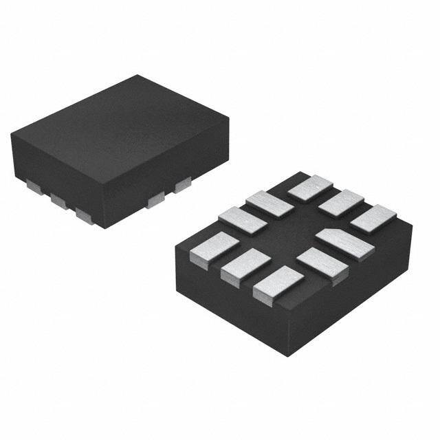
 Datasheet下载
