ICGOO在线商城 > 集成电路(IC) > 线性 - 音頻放大器 > INA137PA
- 型号: INA137PA
- 制造商: Texas Instruments
- 库位|库存: xxxx|xxxx
- 要求:
| 数量阶梯 | 香港交货 | 国内含税 |
| +xxxx | $xxxx | ¥xxxx |
查看当月历史价格
查看今年历史价格
INA137PA产品简介:
ICGOO电子元器件商城为您提供INA137PA由Texas Instruments设计生产,在icgoo商城现货销售,并且可以通过原厂、代理商等渠道进行代购。 INA137PA价格参考。Texas InstrumentsINA137PA封装/规格:线性 - 音頻放大器, Amplifier IC 1-Channel (Mono) Class AB 8-PDIP。您可以下载INA137PA参考资料、Datasheet数据手册功能说明书,资料中有INA137PA 详细功能的应用电路图电压和使用方法及教程。
| 参数 | 数值 |
| 产品目录 | 集成电路 (IC)半导体 |
| 描述 | IC AUDIO DIFF RCVR 8-DIP音频发送器、接收器、收发器 Aud Diff Line Rcvrs +-6dB (G=1/2 or 2) |
| 产品分类 | 线性 - 音频处理集成电路 - IC |
| 品牌 | Texas Instruments |
| 产品手册 | |
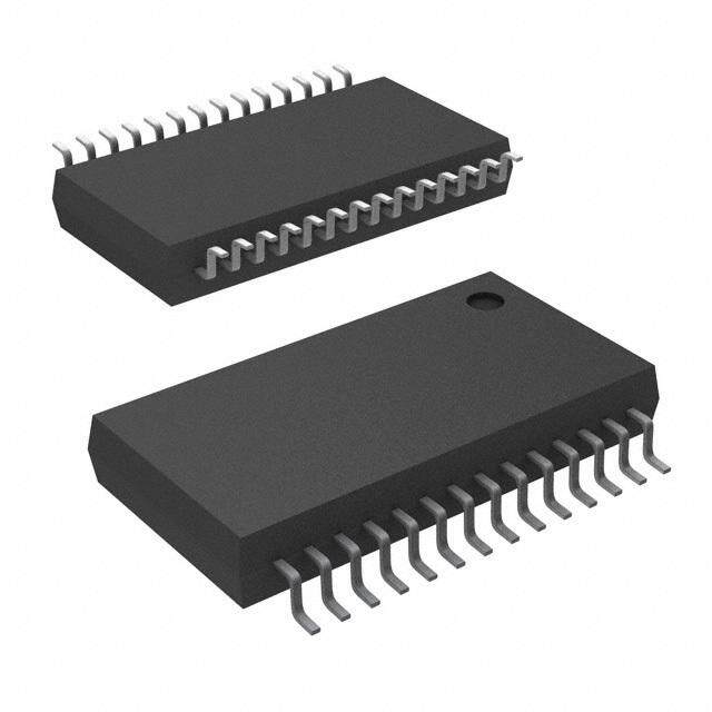
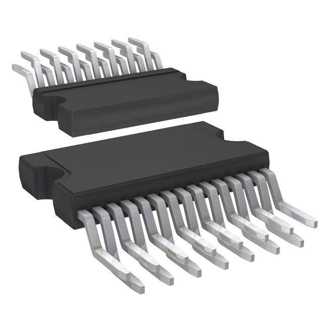
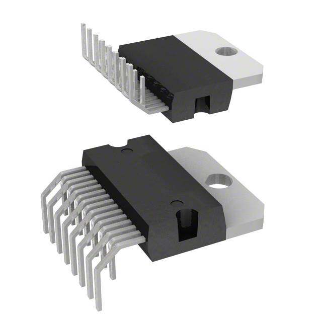
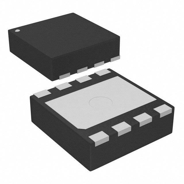
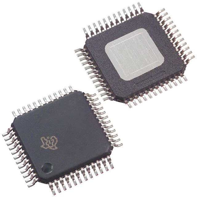
| 产品图片 |
|
| rohs | 符合RoHS无铅 / 符合限制有害物质指令(RoHS)规范要求 |
| 产品系列 | 音频 IC,音频发送器、接收器、收发器,Texas Instruments INA137PA- |
| 数据手册 | |
| 产品型号 | INA137PA |
| 产品目录页面 | |
| 产品种类 | 音频发送器、接收器、收发器 |
| 供应商器件封装 | 8-PDIP |
| 包装 | 管件 |
| 单位重量 | 523.200 mg |
| 商标 | Texas Instruments |
| 安装类型 | 通孔 |
| 安装风格 | Through Hole |
| 封装 | Tube |
| 封装/外壳 | 8-DIP(0.300",7.62mm) |
| 封装/箱体 | PDIP-8 |
| 工作电源电压 | 4 V to 18 V |
| 工厂包装数量 | 50 |
| 应用 | 分流监控器 |
| 最大工作温度 | + 85 C |
| 最小工作温度 | - 40 C |
| 标准包装 | 50 |
| 电源电流 | 2.4 mA |
| 类型 | 线路接收器 |
| 系列 | INA137 |
| 通道数量 | 1 Channel |



PDF Datasheet 数据手册内容提取
® INA137 INA137 INA2137 INA2137 INA137 INA2137 AUDIO DIFFERENTIAL LINE RECEIVERS – 6dB (G = 1/2 or 2) FEATURES APPLICATIONS l SINGLE AND DUAL VERSIONS l AUDIO DIFFERENTIAL LINE RECEIVER l LOW DISTORTION: 0.0005% at f = 1kHz l G = 1/2 OR G = 2 AMPLIFIER l HIGH SLEW RATE: 14V/m s l INSTRUMENTATION BUILDING BLOCK l FAST SETTLING TIME: 3m s to 0.01% l CURRENT SHUNT MONITOR l WIDE SUPPLY RANGE: – 4V to – 18V l VOLTAGE-CONTROLLED CURRENT l LOW QUIESCENT CURRENT: 2.9mA max SOURCE l HIGH CMRR: 90dB l GROUND LOOP ELIMINATOR l FIXED GAIN = – 6dB V+ l PACKAGES—SINGLE: 8-PIN DIP, SO-8 7 DUAL: 14-PIN DIP, SO-14 12kW 6kW 2 5 –In Sense DESCRIPTION The INA137 and INA2137 are differential line receivers 6 Output consisting of high performance op amps with on-chip precision resistors. They are fully specified for high 12kW 6kW 3 1 performance audio applications and have excellent ac +In Ref specifications, including low distortion (0.0005% at INA137 1kHz) and high slew rate (14V/m s), assuring good 4 V+ dynamic response. In addition, wide output voltage V– 11 swing and high output drive capability allow use in a 12kW 6kW wide variety of demanding applications. The dual ver- 2 12 –In A Sense A sion features completely independent circuitry for low- est crosstalk and freedom from interaction, even when overdriven or overloaded. A 13 Out A The INA137 and INA2137 on-chip resistors are laser trimmed for accurate gain and optimum 3 12kW 6kW 14 +In A Ref A common-mode rejection. Furthermore, excellent TCR tracking of the resistors maintains gain accuracy and 12kW 6kW 6 10 –In B Sense B common-mode rejection over temperature. Operation is guaranteed from – 4V to – 18V (8V to 36V total supply). 9 B Out B The INA137 is available in 8-pin DIP and SO-8 surface-mount packages. The INA2137 comes in 12kW 6kW 5 8 +In B Ref B 14-pin DIP and SO-14 surface-mount packages. Both are specified for operation over the extended industrial INA2137 temperature range, –40(cid:176) C to +85(cid:176) C. 4 V– International Airport Industrial Park • Mailing Address: PO Box 11400, Tucson, AZ 85734 • Street Address: 6730 S. Tucson Blvd., Tucson, AZ 85706 • Tel: (520) 746-1111 • Twx: 910-952-1111 Internet: http://www.burr-brown.com/ • FAXLine: (800) 548-6133 (US/Canada Only) • Cable: BBRCORP • Telex: 066-6491 • FAX: (520) 889-1510 • Immediate Product Info: (800) 548-6132 ©1997 Burr-Brown Corporation PDS-1391B Printed in U.S.A. July, 1997 SBOS072
– SPECIFICATIONS: V = 18V S At TA = +25(cid:176)C, VS = – 18V, RL = 2kW , G = 1/2, and Ref Pin connected to Ground, unless otherwise noted. INA137PA, UA INA2137PA, UA PARAMETER CONDITIONS MIN TYP MAX UNITS AUDIO PERFORMANCE Total Harmonic Distortion + Noise, f = 1kHz V = 10Vrms 0.0005 % IN Noise Floor, RTO(1) 20kHz BW –106 dBu Headroom, RTO(1) THD+N < 1% +23 dBu FREQUENCY RESPONSE Small-Signal Bandwidth 4.0 MHz Slew Rate 14 V/m s Settling Time: 0.1% 10V Step, CL = 100pF 2 m s 0.01% 10V Step, C = 100pF 3 m s L Overload Recovery Time 50% Overdrive 3 m s ChannelSeparation (dual), f = 1kHz 123 dB OUTPUT NOISE VOLTAGE(2) f = 20Hz to 20kHz 3.5 m Vrms f = 1kHz 26 nV/(cid:214) HZ OFFSET VOLTAGE(3) RTO Input Offset Voltage VCM = 0V – 100 – 1000 m V vs Temperature Specified Temperature Range – 2 m V/(cid:176)C vs Power Supply VS = – 4V to – 18V – 5 – 60 m V/V INPUT Common-Mode Voltage Range: Positive V = 0V 3(V+)–7.5 3(V+)–6 V O Negative VO = 0V 3(V–)+7.5 3(V–)+3 V Differential Voltage Range See Typical Curve Common-Mode Rejection VCM = – 46.5V, RS = 0W 74 90 dB Impedance(4) Differential 24 kW Common-Mode 18 kW GAIN Initial 0.5 V/V Error V = –10V to 10V – 0.01 – 0.1 % O vs Temperature – 1 – 10 ppm/(cid:176)C Nonlinearity VO = –10V to 10V 0.0001 % OUTPUT Voltage Output, Positive (V+)–2 (V+)–1.8 V Negative (V–)+2 (V–)+1.6 V Current Limit, Continuous to Common – 60 mA Capacitive Load (Stable Operation) 500 pF POWER SUPPLY Rated Voltage – 18 V Voltage Range – 4 – 18 V Quiescent Current (per Amplifier) I = 0 – 2.4 – 2.9 mA O TEMPERATURE RANGE Specification Range –40 85 (cid:176)C Operation Range –55 125 (cid:176)C Storage Range –55 125 (cid:176)C Thermal Resistance, q JA 8-Pin DIP 100 (cid:176)C/W SO-8 Surface-Mount 150 (cid:176)C/W 14-Pin DIP 80 (cid:176)C/W SO-14 Surface-Mount 100 (cid:176)C/W RTO = Referred to Output. NOTES: (1) dBu = 20log (Vrms/0.7746). (2) Includes effects of amplifier’s input current noise and thermal noise contribution of resistor network. (3) Includes effects of amplifier’s input bias and offset currents. (4) Internal resistors are ratio matched but have – 25% absolute value. The information provided herein is believed to be reliable; however, BURR-BROWN assumes no responsibility for inaccuracies or omissions. BURR-BROWN assumes no responsibility for the use of this information, and all use of such information shall be entirely at the user’s own risk. Prices and specifications are subject to change without notice. No patent rights or licenses to any of the circuits described herein are implied or granted to any third party. BURR-BROWN does not authorize or warrant any BURR-BROWN product for use in life support devices and/or systems. ® INA137, INA2137 2
PIN CONFIGURATIONS Top View 8-Pin DIP/SO-8 Top View 14-Pin DIP/SO-14 Ref 1 8 NC NC 1 14 Ref A –In 2 7 V+ –In A 2 13 Out A A +In 3 6 Output +In A 3 12 Sense A V– 4 5 Sense V– 4 11 V+ +In B 5 10 Sense B NC = No Connection B –In B 6 9 Out B ABSOLUTE MAXIMUM RATINGS(1) NC 7 8 Ref B Supply Voltage, V+ to V–....................................................................40V Input Voltage Range..........................................................................– 80V Output Short-Circuit (to ground)(2)............................................................Continuous Operating Temperature.................................................–55(cid:176)C to +125(cid:176)C NC = No Connection Storage Temperature.....................................................–55(cid:176)C to +125(cid:176)C Junction Temperature....................................................................+150(cid:176)C Lead Temperature (soldering, 10s)...............................................+300(cid:176)C NOTE: (1) Stresses above these ratings may cause permanent damage. ELECTROSTATIC (2) One channel per package. DISCHARGE SENSITIVITY PACKAGE/ORDERING INFORMATION This integrated circuit can be damaged by ESD. Burr-Brown PACKAGE SPECIFICATION recommends that all integrated circuits be handled with ap- DRAWING TEMPERATURE propriate precautions. Failure to observe proper handling and PRODUCT PACKAGE NUMBER(1) RANGE installation procedures can cause damage. Single INA137PA 8-Pin DIP 006 –40(cid:176)C to +85(cid:176)C ESD damage can range from subtle performance degradation INA137UA SO-8 Surface-Mount 182 –40(cid:176)C to +85(cid:176)C to complete device failure. Precision integrated circuits may Dual be more susceptible to damage because very small parametric INA2137PA 14-Pin DIP 010 –40(cid:176)C to +85(cid:176)C INA2137UA SO-14 Surface-Mount 235 –40(cid:176)C to +85(cid:176)C changes could cause the device not to meet its published specifications. NOTE: (1) For detailed drawing and dimension table, please see end of data sheet, or Appendix C of Burr-Brown IC Data Book. ® 3 INA137, INA2137
TYPICAL PERFORMANCE CURVES At T = +25(cid:176)C, V = – 18V, and G = 1/2, unless otherwise noted. A S TOTAL HARMONIC DISTORTION+NOISE DIM INTERMODULATION DISTORTION vs FREQUENCY vs OUTPUT AMPLITUDE 0.1 5 BW = 100kHz V = 5Vrms O 1 %) 0.010 RTO D+Noise ( R R= L2 =k W100kW DIM (%) 0.1 RL = 2kW , 600W H 0.001 L T 0.010 R = 600W L 0.0001 0.001 20 100 1k 10k 20k –10 –5 0 5 10 15 20 25 Frequency (Hz) Output Amplitude (dBu) HEADROOM - TOTAL HARMONIC DISTORTION+NOISE HARMONIC DISTORTION PRODUCTS vs OUTPUT AMPLITUDE vs FREQUENCY 1 0.001 V = 1Vrms R = 2kW O L f = 1kHz %) 0.1 RTO damental) 0.0001 2nd Harmonic RL = 600W +Noise ( 0.010 RL = 600W % of Fun 3rd Harmonic R = 2kW HD e ( 0.00001 L T 0.001 RL = 2kW, mplitud RL = 600W 100kW A ( Noise Limited) 0.0001 0.000001 0 5 10 15 20 25 30 20 100 1k 10k 20k Output Amplitude (dBu) Frequency (Hz) OUTPUT VOLTAGE NOISE SPECTRAL DENSITY OUTPUT NOISE VOLTAGE vs FREQUENCY vs NOISE BANDWIDTH 10k 100 Hz) 1k ms) 10 (cid:214)V/ Vr Noise (n oltage (µ Voltage 100 Noise V 1 10 0.1 1 10 100 1k 10k 100k 1M 1 10 100 1k 10k 100k Frequency (Hz) Frequency (Hz) ® INA137, INA2137 4
TYPICAL PERFORMANCE CURVES (CONT) At T = +25(cid:176)C, V = – 18V, and G = 1/2, unless otherwise noted. A S GAIN vs FREQUENCY COMMON-MODE REJECTION vs FREQUENCY 10 100 B) 0 n (d dB) ctio 80 age Gain ( –10 Mode Reje olt n- 60 V –20 mo m Co RTO –30 40 1k 10k 100k 1M 10M 1k 10k 100k 1M Frequency (Hz) Frequency (Hz) POWER SUPPLY REJECTION vs FREQUENCY CHANNEL SEPARATION vs FREQUENCY 120 130 RTO RL = 100kW B) 100 y Rejection (d 8600 –PSR eparation (dB) 112100 RL = 2kW pl S wer Sup 40 +PSR Channel 100 o 20 P Dual Devices 0 90 100 1k 10k 100k 1M 20 100 1k 10k 20k Frequency (Hz) Frequency (Hz) INPUT COMMON-MODE VOLTAGE MAXIMUM OUTPUT VOLTAGE vs FREQUENCY vs OUTPUT VOLTAGE 40 80 G = 1/2 60 VS = ±18V p) 30 e (V) 40 e (Vp- Voltag 20 oltag 20 ode 0 V M Output 10 mmon- ––2400 o C –60 VREF = 0V R = 2kW L 0 –80 100 1k 10k 100k 1M 10M –20 –15 –10 –5 0 5 10 15 20 Frequency (Hz) Output Voltage (V) ® 5 INA137, INA2137
TYPICAL PERFORMANCE CURVES (CONT) At T = +25(cid:176)C, V = – 18V, and G = 1/2, unless otherwise noted. A S QUIESCENT CURRENT vs TEMPERATURE SLEW RATE vs TEMPERATURE 4 16 –SR A) 3 14 ent (m V/µs) +SR urr 2 e ( 12 ent C w Rat uiesc 1 Sle 10 Q 0 8 –75 –50 –25 0 25 50 75 100 125 –75 –50 –25 0 25 50 75 100 125 Temperature (°C) Temperature (°C) SHORT-CIRCUIT CURRENT vs TEMPERATURE QUIESCENT CURRENT vs SUPPLY VOLTAGE 80 3 60 ent (mA) 4200 +ISC nt (mA) 2 Curr 0 urre ort-Circuit ––2400 –ISC uiescent C 1 h Q S –60 –80 0 –75 –50 –25 0 25 50 75 100 125 ±4 ±6 ±8 ±10 ±12 ±14 ±16 ±18 Temperature (°C) Supply Voltage (V) OFFSET VOLTAGE OFFSET VOLTAGE DRIFT PRODUCTION DISTRIBUTION PRODUCTION DISTRIBUTION 35 30 Typical Production Distribution Typical Production 30 Distribution of 25 of Packaged Units. %) Packaged Units. %) ers ( 25 ers ( 20 plifi 20 plifi m m 15 A A of 15 of nt nt 10 ce 10 ce er er P P 5 5 0 0 000000000000000000000 051525354555657585950 00908070605040302010 10203040506070809000 0. 1. 2. 3. 4. 5. 6. 7. 8. 9.1 1––––––––– 1 – Offset Voltage (µV) Offset Voltage Drift (µV/°C) ® INA137, INA2137 6
TYPICAL PERFORMANCE CURVES (CONT) At T = +25(cid:176)C, V = – 18V, and G = 1/2, unless otherwise noted. A S SMALL-SIGNAL OVERSHOOT OUTPUT VOLTAGE SWING vs OUTPUT CURRENT vs LOAD CAPACITANCE 17 70 16 –55°C 60 15 V) 25°C g ( 14 125°C 50 utput Voltage Swin –––1111132234 85°C125°C 85°C Overshoot (%) 432000 O –15 R = 2kW 25°C 10 L –16 –55°C 100mV Step –17 0 0 ±20 ±40 ±60 ±80 0 200 400 600 800 1000 1200 Output Current (mA) Load Capacitance (pF) LARGE-SIGNAL STEP RESPONSE C = 100pF SMALL-SIGNAL STEP RESPONSE L C = 100pF L v mV/di V/div 0 5 5 C = 500pF L 1m s/div 1m s/div ® 7 INA137, INA2137
APPLICATIONS INFORMATION The INA137 and INA2137 have excellent distortion charac- teristics. THD+Noise is below 0.001% throughout the audio The INA137 and INA2137 are differential line receivers frequency range. Up to approximately 10kHz distortion is suitable for a wide range of audio and general-purpose below the measurement limit of commonly used test equip- applications. Figure 1 shows the basic G = 1/2 (–6dB) ment. Furthermore, distortion remains relatively flat over its differential receiver configuration. The input and feedback wide output voltage swing range (approximately 1.7V from resistors can be reversed to achieve G = 2 (+6dB), as shown either supply). in Figure 2. For applications requiring G = 1 (0dB), the INA134 and INA2134 are recommended. OFFSET VOLTAGE TRIM Decoupling capacitors are strongly recommended for appli- The INA137 and INA2137 are laser trimmed for low offset cations with noisy or high impedance power supplies. The voltage and drift. Most applications require no external offset capacitors should be placed close to the device pins as adjustment. Figure 3 shows an optional circuit for trimming shown in Figure 1. All circuitry is completely independent the output offset voltage. The output is referred to the output in the dual version assuring lowest crosstalk and normal reference terminal (pin 1), which is normally grounded. A behavior when one amplifier is overdriven or short-cir- voltage applied to the Ref terminal will be summed with the cuited. output signal. This can be used to null offset voltage as As shown in Figure 1, the differential input signal is con- shown in Figure 3. The source impedance of a signal applied nected to pins 2 and 3. The source impedances connected to to the Ref terminal should be less than 10W to maintain good the inputs must be nearly equal to assure good common- common-mode rejection. mode rejection. A 5W mismatch in source impedance will degrade the common-mode rejection of a typical device to approximately 77dB (RTO). If the source has a known impedance mismatch, an additional resistor in series with INA137 the opposite input can be used to preserve good common- R R mode rejection. –In 5 2 1 2 V 2 6kW 12kW V– V+ 6 1µF 1µF VO = 2 (V3 – V2) R R 4 7 +In 1 4 3 3 V INA137 3 6kW 12kW R R –In 1 2 2 5 V 2 12kW 6kW FIGURE 2. G = 2 Differential Receiver. 6 VO = 1/2 (V3 – V2) G = 1/2 INA137 +In 3 R3 R4 1 12Rk1W 6RkW2 V 2 5 3 V 12kW 6kW 2 6 V FIGURE 1. G = 1/2 Differential Receiver (Basic Power O Supply and Signal Connections). R 3 20W 12kW 3 V 3 AUDIO PERFORMANCE R The INA137 and INA2137 were designed for enhanced ac 6kW4 performance. Very low distortion, low noise, and wide band- +15V width provide superior performance in high quality audio 1 applications. Laser-trimmed matched resistors provide opti- VO = 1/2 (V3 – V2) 250kW Offset Adjustment 100kW mum common-mode rejection (typically 90dB), especially Range = ±1mV when compared to circuits implemented with an op amp 10W and discrete precision resistors. In addition, high slew rate (14V/m s) and fast settling time (3m s to 0.01%) ensure excel- –15V lent dynamic performance. FIGURE 3. Offset Adjustment. ® INA137, INA2137 8
INA137 6kW 12kW G = 2 INA137 2 5 V 1 6kW 12kW –In 1/2 2 5 OPA2134 6 1 6kW V0 = 2V1 + V2 R2 V 1 12kW V2 3 R1 6 V R 0 2 0utput FIGURE 4. Precision Summing Amplifier. 6kW 12kW 1/2 3 1 V OPA2134 2 INA137 +In 12kW 6kW 2 5 –In V = 2 (1 + 2R/R) (V –V) O 2 1 2 1 6 3 6 BUF634 VO FIGURE 6. High Input Impedance Instrumentation Amplifier. 12kW 6kW 3 1 +In FIGURE 5. Boosting Output Current. The difference amplifier is a highly versatile building •Precision Voltage-to-Current Converter with Differential block that is useful in a wide variety of applications. See Inputs the INA105 data sheet for additional applications ideas, •Differential Input Voltage-to-Current Converter for Low including: I OUT •Current Receiver with Compliance to Rails •Isolating Current Source •– 10V Precision Voltage Reference •Differential Output Difference Amplifier •– 5V Precision Voltage Reference •Isolating Current Source with Buffering Amplifier for •Precision Average Value Amplifier Greater Accuracy •Precision Bipolar Offsetting •Window Comparator with Window Span and Window Center Inputs •Precision Summing Amplifier with Gain •Precision Voltage-Controlled Current Source with Buff- •Instrumentation Amplifier Guard Drive Generator ered Differential Inputs and Gain •Precision Summing Instrumentation Amplifier •Precision Absolute Value Buffer ® 9 INA137, INA2137
PACKAGE OPTION ADDENDUM www.ti.com 16-Feb-2009 PACKAGING INFORMATION OrderableDevice Status(1) Package Package Pins Package EcoPlan(2) Lead/BallFinish MSLPeakTemp(3) Type Drawing Qty INA137PA ACTIVE PDIP P 8 50 Green(RoHS& CUNIPDAU N/AforPkgType noSb/Br) INA137PAG4 ACTIVE PDIP P 8 50 Green(RoHS& CUNIPDAU N/AforPkgType noSb/Br) INA137UA ACTIVE SOIC D 8 75 Green(RoHS& CUNIPDAU Level-3-260C-168HR noSb/Br) INA137UA/2K5 ACTIVE SOIC D 8 2500 Green(RoHS& CUNIPDAU Level-3-260C-168HR noSb/Br) INA137UA/2K5G4 ACTIVE SOIC D 8 2500 Green(RoHS& CUNIPDAU Level-3-260C-168HR noSb/Br) INA137UAG4 ACTIVE SOIC D 8 75 Green(RoHS& CUNIPDAU Level-3-260C-168HR noSb/Br) INA2137PA ACTIVE PDIP N 14 25 Green(RoHS& CUNIPDAU N/AforPkgType noSb/Br) INA2137PAG4 ACTIVE PDIP N 14 25 Green(RoHS& CUNIPDAU N/AforPkgType noSb/Br) INA2137UA ACTIVE SOIC D 14 50 Green(RoHS& CUNIPDAU Level-3-260C-168HR noSb/Br) INA2137UA/2K5 ACTIVE SOIC D 14 2500 Green(RoHS& CUNIPDAU Level-3-260C-168HR noSb/Br) INA2137UA/2K5E4 ACTIVE SOIC D 14 2500 Green(RoHS& CUNIPDAU Level-3-260C-168HR noSb/Br) INA2137UAE4 ACTIVE SOIC D 14 50 Green(RoHS& CUNIPDAU Level-3-260C-168HR noSb/Br) (1)Themarketingstatusvaluesaredefinedasfollows: ACTIVE:Productdevicerecommendedfornewdesigns. LIFEBUY:TIhasannouncedthatthedevicewillbediscontinued,andalifetime-buyperiodisineffect. NRND:Notrecommendedfornewdesigns.Deviceisinproductiontosupportexistingcustomers,butTIdoesnotrecommendusingthispartin anewdesign. PREVIEW:Devicehasbeenannouncedbutisnotinproduction.Samplesmayormaynotbeavailable. OBSOLETE:TIhasdiscontinuedtheproductionofthedevice. (2)EcoPlan-Theplannedeco-friendlyclassification:Pb-Free(RoHS),Pb-Free(RoHSExempt),orGreen(RoHS&noSb/Br)-pleasecheck http://www.ti.com/productcontentforthelatestavailabilityinformationandadditionalproductcontentdetails. TBD:ThePb-Free/Greenconversionplanhasnotbeendefined. Pb-Free(RoHS):TI'sterms"Lead-Free"or"Pb-Free"meansemiconductorproductsthatarecompatiblewiththecurrentRoHSrequirements forall6substances,includingtherequirementthatleadnotexceed0.1%byweightinhomogeneousmaterials.Wheredesignedtobesoldered athightemperatures,TIPb-Freeproductsaresuitableforuseinspecifiedlead-freeprocesses. Pb-Free(RoHSExempt):ThiscomponenthasaRoHSexemptionforeither1)lead-basedflip-chipsolderbumpsusedbetweenthedieand package, or 2) lead-based die adhesive used between the die and leadframe. The component is otherwise considered Pb-Free (RoHS compatible)asdefinedabove. Green(RoHS&noSb/Br):TIdefines"Green"tomeanPb-Free(RoHScompatible),andfreeofBromine(Br)andAntimony(Sb)basedflame retardants(BrorSbdonotexceed0.1%byweightinhomogeneousmaterial) (3) MSL, Peak Temp. -- The Moisture Sensitivity Level rating according to the JEDEC industry standard classifications, and peak solder temperature. Important Information and Disclaimer:The information provided on this page represents TI's knowledge and belief as of the date that it is provided. TI bases its knowledge and belief on information provided by third parties, and makes no representation or warranty as to the accuracy of such information. Efforts are underway to better integrate information from third parties. TI has taken and continues to take reasonable steps to provide representative and accurate information but may not have conducted destructive testing or chemical analysis on incomingmaterialsandchemicals.TIandTIsuppliersconsidercertaininformationtobeproprietary,andthusCASnumbersandotherlimited informationmaynotbeavailableforrelease. Addendum-Page1
PACKAGE OPTION ADDENDUM www.ti.com 16-Feb-2009 InnoeventshallTI'sliabilityarisingoutofsuchinformationexceedthetotalpurchasepriceoftheTIpart(s)atissueinthisdocumentsoldbyTI toCustomeronanannualbasis. Addendum-Page2
PACKAGE MATERIALS INFORMATION www.ti.com 11-Mar-2008 TAPE AND REEL INFORMATION *Alldimensionsarenominal Device Package Package Pins SPQ Reel Reel A0(mm) B0(mm) K0(mm) P1 W Pin1 Type Drawing Diameter Width (mm) (mm) Quadrant (mm) W1(mm) INA137UA/2K5 SOIC D 8 2500 330.0 12.4 6.4 5.2 2.1 8.0 12.0 Q1 INA2137UA/2K5 SOIC D 14 2500 330.0 16.4 6.5 9.0 2.1 8.0 16.0 Q1 PackMaterials-Page1
PACKAGE MATERIALS INFORMATION www.ti.com 11-Mar-2008 *Alldimensionsarenominal Device PackageType PackageDrawing Pins SPQ Length(mm) Width(mm) Height(mm) INA137UA/2K5 SOIC D 8 2500 346.0 346.0 29.0 INA2137UA/2K5 SOIC D 14 2500 346.0 346.0 33.0 PackMaterials-Page2
IMPORTANTNOTICE TexasInstrumentsIncorporatedanditssubsidiaries(TI)reservetherighttomakecorrections,modifications,enhancements,improvements, andotherchangestoitsproductsandservicesatanytimeandtodiscontinueanyproductorservicewithoutnotice.Customersshould obtainthelatestrelevantinformationbeforeplacingordersandshouldverifythatsuchinformationiscurrentandcomplete.Allproductsare soldsubjecttoTI’stermsandconditionsofsalesuppliedatthetimeoforderacknowledgment. TIwarrantsperformanceofitshardwareproductstothespecificationsapplicableatthetimeofsaleinaccordancewithTI’sstandard warranty.TestingandotherqualitycontroltechniquesareusedtotheextentTIdeemsnecessarytosupportthiswarranty.Exceptwhere mandatedbygovernmentrequirements,testingofallparametersofeachproductisnotnecessarilyperformed. TIassumesnoliabilityforapplicationsassistanceorcustomerproductdesign.Customersareresponsiblefortheirproductsand applicationsusingTIcomponents.Tominimizetherisksassociatedwithcustomerproductsandapplications,customersshouldprovide adequatedesignandoperatingsafeguards. TIdoesnotwarrantorrepresentthatanylicense,eitherexpressorimplied,isgrantedunderanyTIpatentright,copyright,maskworkright, orotherTIintellectualpropertyrightrelatingtoanycombination,machine,orprocessinwhichTIproductsorservicesareused.Information publishedbyTIregardingthird-partyproductsorservicesdoesnotconstitutealicensefromTItousesuchproductsorservicesora warrantyorendorsementthereof.Useofsuchinformationmayrequirealicensefromathirdpartyunderthepatentsorotherintellectual propertyofthethirdparty,oralicensefromTIunderthepatentsorotherintellectualpropertyofTI. ReproductionofTIinformationinTIdatabooksordatasheetsispermissibleonlyifreproductioniswithoutalterationandisaccompanied byallassociatedwarranties,conditions,limitations,andnotices.Reproductionofthisinformationwithalterationisanunfairanddeceptive businesspractice.TIisnotresponsibleorliableforsuchaltereddocumentation.Informationofthirdpartiesmaybesubjecttoadditional restrictions. ResaleofTIproductsorserviceswithstatementsdifferentfromorbeyondtheparametersstatedbyTIforthatproductorservicevoidsall expressandanyimpliedwarrantiesfortheassociatedTIproductorserviceandisanunfairanddeceptivebusinesspractice.TIisnot responsibleorliableforanysuchstatements. TIproductsarenotauthorizedforuseinsafety-criticalapplications(suchaslifesupport)whereafailureoftheTIproductwouldreasonably beexpectedtocauseseverepersonalinjuryordeath,unlessofficersofthepartieshaveexecutedanagreementspecificallygoverning suchuse.Buyersrepresentthattheyhaveallnecessaryexpertiseinthesafetyandregulatoryramificationsoftheirapplications,and acknowledgeandagreethattheyaresolelyresponsibleforalllegal,regulatoryandsafety-relatedrequirementsconcerningtheirproducts andanyuseofTIproductsinsuchsafety-criticalapplications,notwithstandinganyapplications-relatedinformationorsupportthatmaybe providedbyTI.Further,BuyersmustfullyindemnifyTIanditsrepresentativesagainstanydamagesarisingoutoftheuseofTIproductsin suchsafety-criticalapplications. TIproductsareneitherdesignednorintendedforuseinmilitary/aerospaceapplicationsorenvironmentsunlesstheTIproductsare specificallydesignatedbyTIasmilitary-gradeor"enhancedplastic."OnlyproductsdesignatedbyTIasmilitary-grademeetmilitary specifications.BuyersacknowledgeandagreethatanysuchuseofTIproductswhichTIhasnotdesignatedasmilitary-gradeissolelyat theBuyer'srisk,andthattheyaresolelyresponsibleforcompliancewithalllegalandregulatoryrequirementsinconnectionwithsuchuse. TIproductsareneitherdesignednorintendedforuseinautomotiveapplicationsorenvironmentsunlessthespecificTIproductsare designatedbyTIascompliantwithISO/TS16949requirements.Buyersacknowledgeandagreethat,iftheyuseanynon-designated productsinautomotiveapplications,TIwillnotberesponsibleforanyfailuretomeetsuchrequirements. FollowingareURLswhereyoucanobtaininformationonotherTexasInstrumentsproductsandapplicationsolutions: Products Applications Amplifiers amplifier.ti.com Audio www.ti.com/audio DataConverters dataconverter.ti.com Automotive www.ti.com/automotive DLP®Products www.dlp.com Broadband www.ti.com/broadband DSP dsp.ti.com DigitalControl www.ti.com/digitalcontrol ClocksandTimers www.ti.com/clocks Medical www.ti.com/medical Interface interface.ti.com Military www.ti.com/military Logic logic.ti.com OpticalNetworking www.ti.com/opticalnetwork PowerMgmt power.ti.com Security www.ti.com/security Microcontrollers microcontroller.ti.com Telephony www.ti.com/telephony RFID www.ti-rfid.com Video&Imaging www.ti.com/video RF/IFandZigBee®Solutions www.ti.com/lprf Wireless www.ti.com/wireless MailingAddress:TexasInstruments,PostOfficeBox655303,Dallas,Texas75265 Copyright©2009,TexasInstrumentsIncorporated

 Datasheet下载


