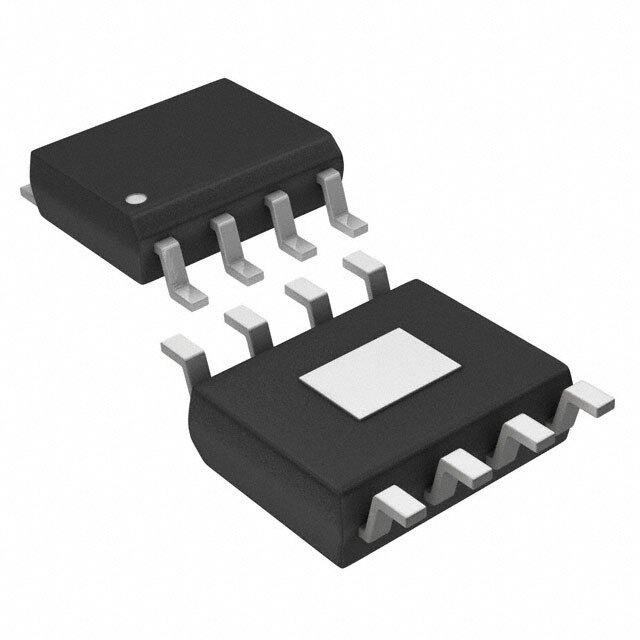
ICGOO在线商城 > IFX1050G
- 型号: IFX1050G
- 制造商: Infineon
- 库位|库存: xxxx|xxxx
- 要求:
| 数量阶梯 | 香港交货 | 国内含税 |
| +xxxx | $xxxx | ¥xxxx |
查看当月历史价格
查看今年历史价格
IFX1050G产品简介:
ICGOO电子元器件商城为您提供IFX1050G由Infineon设计生产,在icgoo商城现货销售,并且可以通过原厂、代理商等渠道进行代购。 提供IFX1050G价格参考¥2.78-¥7.66以及InfineonIFX1050G封装/规格参数等产品信息。 你可以下载IFX1050G参考资料、Datasheet数据手册功能说明书, 资料中有IFX1050G详细功能的应用电路图电压和使用方法及教程。
| 参数 | 数值 |
| 产品目录 | 集成电路 (IC)半导体 |
| 描述 | IC TXRX CAN 5V HS DSO-8CAN 接口集成电路 High Speed CAN Transceiver |
| 产品分类 | |
| 品牌 | Infineon Technologies |
| 产品手册 | |
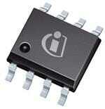
| 产品图片 |
|
| rohs | 符合RoHS无铅 / 符合限制有害物质指令(RoHS)规范要求 |
| 产品系列 | 接口 IC,CAN 接口集成电路,Infineon Technologies IFX1050G- |
| 数据手册 | http://www.infineon.com/dgdl/IFX1050G_DS_rev10.pdf?folderId=db3a30431ed1d7b2011edadb13813703&fileId=db3a304320d39d590121f374ea660d66&ack=t |
| 产品型号 | IFX1050G |
| PCN封装 | |
| 产品种类 | CAN 接口集成电路 |
| 供应商器件封装 | PG-DSO-8 |
| 其它名称 | IFX1050GINTR |
| 包装 | 带卷 (TR) |
| 协议 | CAN |
| 双工 | 全 |
| 商标 | Infineon Technologies |
| 安装类型 | 表面贴装 |
| 安装风格 | SMD/SMT |
| 封装 | Reel |
| 封装/外壳 | 8-SOIC(0.154",3.90mm 宽) |
| 封装/箱体 | PG-DSO-8 |
| 工作温度 | -40°C ~ 125°C |
| 工作温度范围 | - 40 C to + 125 C |
| 工作电源电压 | 4.5 V to 5.5 V |
| 工厂包装数量 | 2500 |
| 接收器滞后 | 150mV |
| 数据速率 | 1MBd |
| 最大工作温度 | + 125 C |
| 标准包装 | 2,500 |
| 电压-电源 | 4.5 V ~ 5.5 V |
| 电源电压-最大 | 5.5 V |
| 电源电压-最小 | 4.5 V |
| 电源电流 | 70 mA |
| 类型 | CAN Transceiver |
| 系列 | IFX1050 |
| 零件号别名 | IFX1050GXUMA1 SP000613990 |
| 驱动器/接收器数 | 1/1 |


PDF Datasheet 数据手册内容提取
IFX1050G High Speed CAN-Transceiver Data Sheet Rev. 1.0, 2009-05-14 Standard Products
IFX1050G Table of Contents Table of Contents 1 Overview . . . . . . . . . . . . . . . . . . . . . . . . . . . . . . . . . . . . . . . . . . . . . . . . . . . . . . . . . . . . . . . . . . . . . . . 3 2 Block Diagram . . . . . . . . . . . . . . . . . . . . . . . . . . . . . . . . . . . . . . . . . . . . . . . . . . . . . . . . . . . . . . . . . . . 4 3 Pin Configuration . . . . . . . . . . . . . . . . . . . . . . . . . . . . . . . . . . . . . . . . . . . . . . . . . . . . . . . . . . . . . . . . 5 3.1 Pin Assignment . . . . . . . . . . . . . . . . . . . . . . . . . . . . . . . . . . . . . . . . . . . . . . . . . . . . . . . . . . . . . . . . . . . 5 3.2 Pin Definitions and Functions . . . . . . . . . . . . . . . . . . . . . . . . . . . . . . . . . . . . . . . . . . . . . . . . . . . . . . . . 5 4 Operation Modes . . . . . . . . . . . . . . . . . . . . . . . . . . . . . . . . . . . . . . . . . . . . . . . . . . . . . . . . . . . . . . . . 6 4.1 Normal Mode . . . . . . . . . . . . . . . . . . . . . . . . . . . . . . . . . . . . . . . . . . . . . . . . . . . . . . . . . . . . . . . . . . . . 6 4.2 Stand-By Mode . . . . . . . . . . . . . . . . . . . . . . . . . . . . . . . . . . . . . . . . . . . . . . . . . . . . . . . . . . . . . . . . . . 6 4.3 Receive-Only Mode . . . . . . . . . . . . . . . . . . . . . . . . . . . . . . . . . . . . . . . . . . . . . . . . . . . . . . . . . . . . . . 6 5 Electrical Characteristics . . . . . . . . . . . . . . . . . . . . . . . . . . . . . . . . . . . . . . . . . . . . . . . . . . . . . . . . . . 7 5.1 Absolute Maximum Ratings . . . . . . . . . . . . . . . . . . . . . . . . . . . . . . . . . . . . . . . . . . . . . . . . . . . . . . . . . 7 5.2 Functional Range . . . . . . . . . . . . . . . . . . . . . . . . . . . . . . . . . . . . . . . . . . . . . . . . . . . . . . . . . . . . . . . . . 7 5.3 Thermal Resistance . . . . . . . . . . . . . . . . . . . . . . . . . . . . . . . . . . . . . . . . . . . . . . . . . . . . . . . . . . . . . . . 7 6 Electrical Characteristics . . . . . . . . . . . . . . . . . . . . . . . . . . . . . . . . . . . . . . . . . . . . . . . . . . . . . . . . . . 8 7 Application Information . . . . . . . . . . . . . . . . . . . . . . . . . . . . . . . . . . . . . . . . . . . . . . . . . . . . . . . . . . 12 7.1 Further Application Information . . . . . . . . . . . . . . . . . . . . . . . . . . . . . . . . . . . . . . . . . . . . . . . . . . . . . . 12 8 Package Outlines . . . . . . . . . . . . . . . . . . . . . . . . . . . . . . . . . . . . . . . . . . . . . . . . . . . . . . . . . . . . . . . 13 9 Revision History . . . . . . . . . . . . . . . . . . . . . . . . . . . . . . . . . . . . . . . . . . . . . . . . . . . . . . . . . . . . . . . . 14 DataSheet 2 Rev. 1.0, 2009-05-14
High Speed CAN-Transceiver IFX1050G 1 Overview Features • CAN data transmission rates from 1kBaud up to 1MBaud • Receive-Only Mode and Stand-By Mode • Optimized Electromagnetic Compatibility (EMC) • Optimized for a high immunity against Electromagnetic Interference (EMI) • Bus pins are short circuit proof • Over-temperature protection PG-DSO-8 • Very wide temperature range (-40 °C up to 125 °C) • Green Product (RoHS compliant) Description The IFX1050G is optimized for high speed differential mode data transmission in industrial applications and it is compliant to ISO11898-2. The transceiver IFX1050G works as an interface between the CAN protocol controller and the physical differential bus in High Speed CAN applications. It supports data transmission rates from 1kBaud up to 1MBaud. The IFX1050G has three different operation modes: The Normal Mode, the Receive-Only Mode and the Stand-By Mode. The mode selection is controlled by the logical input pins RM and INH. The IC is based on the Smart Power Technology SPT® which allows bipolar and CMOS control circuitry in accordance with DMOS power devices existing on the same monolithic circuit. The IFX1050G is designed to withstand the severe conditions in industrial applications and provides excellent EMC performance within a broad frequency range. Type Package Marking IFX1050G PG-DSO-8 IFX1050G DataSheet 3 Rev. 1.0, 2009-05-14
IFX1050G Block Diagram 2 Block Diagram (cid:22) (cid:57) (cid:38)(cid:38) (cid:26) (cid:39)(cid:85)(cid:76)(cid:89)(cid:72)(cid:85) (cid:38)(cid:36)(cid:49)(cid:43) (cid:50)(cid:88)(cid:87)(cid:83)(cid:88)(cid:87) (cid:20) (cid:55)(cid:91)(cid:39) (cid:25) (cid:54)(cid:87)(cid:68)(cid:74)(cid:72) (cid:55)(cid:72)(cid:80)(cid:83)(cid:16) (cid:38)(cid:36)(cid:49)(cid:47) (cid:51)(cid:85)(cid:82)(cid:87)(cid:72)(cid:70)(cid:87)(cid:76)(cid:82)(cid:81) (cid:27) (cid:48)(cid:82)(cid:71)(cid:72)(cid:3)(cid:38)(cid:82)(cid:81)(cid:87)(cid:85)(cid:82)(cid:79) (cid:44)(cid:49)(cid:43) (cid:24) (cid:53)(cid:48) (cid:32) (cid:53)(cid:72)(cid:70)(cid:72)(cid:76)(cid:89)(cid:72)(cid:85) (cid:13) (cid:23) (cid:53)(cid:91)(cid:39) (cid:21) (cid:42)(cid:49)(cid:39) Figure1 Block Diagram DataSheet 4 Rev. 1.0, 2009-05-14
IFX1050G Pin Configuration 3 Pin Configuration 3.1 Pin Assignment (cid:55)(cid:91)(cid:39) (cid:20) (cid:27) (cid:44)(cid:49)(cid:43) (cid:42)(cid:49)(cid:39) (cid:21) (cid:26) (cid:38)(cid:36)(cid:49)(cid:43) (cid:57) (cid:22) (cid:25) (cid:38)(cid:36)(cid:49)(cid:47) (cid:38)(cid:38) (cid:53)(cid:91)(cid:39) (cid:23) (cid:24) (cid:53)(cid:48) (cid:51)(cid:44)(cid:49)(cid:38)(cid:50)(cid:49)(cid:41)(cid:44)(cid:42)(cid:66)(cid:44)(cid:41)(cid:59)(cid:20)(cid:19)(cid:24)(cid:19)(cid:17)(cid:54)(cid:57)(cid:42) Figure2 Pin Configuration 3.2 Pin Definitions and Functions Pin Symbol Function 1 TxD CAN transmit data input; 20 kΩ pull-up, “LOW” in dominant state 2 GND Ground 3 V 5V Supply input CC 4 RxD CAN receive data output; “LOW” in dominant state, integrated pull-up 5 RM Receive-Only input; control input, integrated 20 kΩ pull-up, “LOW” to activate Receive-Only Mode 6 CANL Low line I/O; “LOW” in dominant state 7 CANH High line I/O; “HIGH” in dominant state 8 INH Inhibit Input; control input, 20 kΩ pull-up, “LOW” to activate Normal Mode DataSheet 5 Rev. 1.0, 2009-05-14
IFX1050G Operation Modes 4 Operation Modes Normal Mode INH = 1 RM = 0 INH = 0 RM = 1 INH = 0 RM = 1 and RM = 1 INH = 0 and RM = 0 Stand-by Mode Receive-only Mode INH = 1 INH = 1 RM = 0 / 1 INH = 0 RM = 0 AED02924 Figure3 Mode State Diagram The IFX1050G is equipped with three different operation modes. 4.1 Normal Mode In the Normal Mode the device is able to receive data from the CANbus and to transmit messages to the CANbus. The IFX1050G enters Normal Mode by setting the INH input to logical “LOW” and the RM input to logical “HIGH” (see Figure3). 4.2 Stand - By Mode Stand-By Mode is a Low-Power mode with reduced current consumption on the power supply V . CC In Stand-By Mode the receiver and the transceiver of the IFX1050G are disabled and the device can not receive any data from the CANbus, nor transmit any data to the CANbus. The IFX1050G enters Stand-By Mode by setting the INH input to logical “HIGH” (see Figure3). When the Stand-By mode is not used the INH pin has to be connected to GND in order to switch the IFX1050G permanently into Normal Mode. 4.3 Receive - Only Mode The Receive-Only Mode can be used for diagnostic purposes (to check the bus connections between the nodes) as well as to prevent the bus being blocked by a faulty permanent dominant TxD input signal. In Receive-Only Mode the output stage of the transceiver IFX1050G is disabled. The IFX1050G can not send any data to the CANbus, but is still able to receive data from the CANbus. The IFX1050G enters Receive-Only Mode by setting the RM input and the INH input to logical “LOW” (see Figure3). In case the Receive-Only Mode is not used, the RM pin can be left open or it can be also connected to the power supply V . CC DataSheet 6 Rev. 1.0, 2009-05-14
IFX1050G Electrical Characteristics 5 Electrical Characteristics 5.1 Absolute Maximum Ratings Table1 Absolute Maximum Ratings Parameter Symbol Limit Values Unit Remarks Min. Max. Voltages Supply voltage V -0.3 6.5 V – CC CAN input voltage (CANH, CANL) V -40 40 V – CANH/L Logic voltages at INH, RM, TxD, RxD V -0.3 V V 0 V < V < 5.5 V I CC CC Electrostatic discharge voltage at V -6 6 kV human body model (100 pF via ESD CANH, CANL 1.5 kΩ) Electrostatic discharge voltage V -2 2 kV human body model (100 pF via ESD 1.5 kΩ) Temperatures Junction temperature T -40 160 °C – j Note:Stresses above the ones listed here may cause permanent damage to the device. Exposure to absolute maximum rating conditions for extended periods may affect device reliability. Note:Integrated protection functions are designed to prevent IC destruction under fault conditions described in the data sheet. Fault conditions are considered as “outside” normal operating range. Protection functions are not designed for continuous repetitive operation. 5.2 Functional Range Table2 Functional Range Parameter Symbol Limit Values Unit Remarks Min. Max. Supply voltage V 4.5 5.5 V – CC Junction temperature T -40 125 °C – j Thermal Shutdown (junction temperature) Thermal shutdown temperature T 160 200 °C 10 °C hysteresis jsD Note:Within the functional or operating range, the IC operates as described in the circuit description. The electrical characteristics are specified within the conditions given in the Electrical Characteristics table. 5.3 Thermal Resistance Pos. Parameter Symbol Limit Values Unit Conditions Min. Typ. Max. 5.3.1 Junction to Ambient1) R – – 185 K/W thJA 1) Not subject to production test, specified by design. DataSheet 7 Rev. 1.0, 2009-05-14
IFX1050G Electrical Characteristics 6 Electrical Characteristics Table3 Electrical Characteristics 4.5 V < V < 5.5 V; R = 60 Ω; V < V ; -40 °C < T < 125 °C; all voltages with respect to ground; positive CC L INH INH,ON j current flowing into pin; unless otherwise specified. Parameter Symbol Limit Values Unit Remarks Min. Typ. Max. Current Consumption Current consumption I – 6 10 mA Recessive state; CC V = V TxD CC Current consumption I – 45 70 mA Dominant state; CC V = 0 V TxD Current consumption I – 6 10 mA Receive-Only Mode; CC RM=“LOW” Current consumption I – 1 10 µA Stand-By Mode; CC,stb TxD=RM=“High” Receiver Output RxD HIGH level output current I – -4 -2 mA V = 0.8 × V , RD,H RD CC V < 0.4 V1) diff LOW level output current I 2 4 – mA V = 0.2 × V , RD,L RD CC V > 1 V1) diff Transmission Input TxD HIGH level input voltage threshold V – 0.5 × 0.7 × V Recessive state TD,H V V CC CC LOW level input voltage threshold V 0.3 × 0.4 × – V Dominant state TD,L V V CC CC TxD pull-up resistance R 10 25 50 kΩ – TD Inhibit Input (pin INH) HIGH level input voltage threshold V – 0.5 × 0.7 × V Stand-By Mode; INH,H V V CC CC LOW level input voltage threshold V 0.3 × 0.4 × – V Normal Mode INH,L V V CC CC INH pull-up resistance R 10 25 50 kΩ – INH Receive only Input (pin RM) HIGH level input voltage threshold V – 0.5 × 0.7 × V Normal Mode RM,H V V CC CC LOW level input voltage threshold V 0.3 × 0.4 × – V Receive-Only Mode RM,L V V CC CC RM pull-up resistance R 10 25 50 kΩ – RM DataSheet 8 Rev. 1.0, 2009-05-14
IFX1050G Electrical Characteristics Table3 Electrical Characteristics (cont’d) 4.5 V < V < 5.5 V; R = 60 Ω; V < V ; -40 °C < T < 125 °C; all voltages with respect to ground; positive CC L INH INH,ON j current flowing into pin; unless otherwise specified. Parameter Symbol Limit Values Unit Remarks Min. Typ. Max. Bus Receiver Differential receiver threshold voltage, V – 0.75 0.90 V -7V < (V , V ) < 12V diff,d CANH CANL recessive to dominant edge V = V - V diff CANH CANL Differential receiver threshold voltage V 0.50 0.60 – V -7V < (V , V ) < 12V diff,r CANH CANL dominant to recessive edge V = V - V diff CANH CANL Common Mode Range CMR -7 – 12 V V = 5 V CC Differential receiver hysteresis V – 150 – mV – diff,hys CANH, CANL input resistance R 10 20 30 kΩ Recessive state i Differential input resistance R 20 40 60 kΩ Recessive state diff Bus Transmitter CANL/CANH recessive output voltage V 0.4 × – 0.6 × V V = V CANL/H TxD CC V V CC CC CANH, CANL recessive output voltage V -1 – 0.05 V V = V diff TxD CC difference V = V - V , no load diff CANH CANL CANL dominant output voltage V – – 2.0 V V = 0 V; CANL TxD V = 5 V CC CANH dominant output voltage V 2.8 – – V V = 0 V; CANH TxD V = 5 V CC CANH, CANL dominant output voltage V 1.5 – 3.0 V V = 0 V; diff TxD difference V = 5 V CC V = V - V diff CANH CANL CANL short circuit current I 50 120 200 mA V = 18 V CANLsc CANLshort CANH short circuit current I -200 -120 -50 mA V = 0 V CANHsc CANHshort Output current CANH/CANL I -50 -300 -400 µA V = 0 V, CANH/L,lk CC V = V = -7 V CANH CANL -50 -100 -150 µA V = 0 V, CC V = V = -2 V CANH CANL Output current CANH/CANL I 50 280 400 µA V = 0 V, CANH/L,lk CC V = V = 7 V CANH CANL 50 100 150 µA V = 0 V, CC V = V = 2 V CANH CANL DataSheet 9 Rev. 1.0, 2009-05-14
IFX1050G Electrical Characteristics Table3 Electrical Characteristics (cont’d) 4.5 V < V < 5.5 V; R = 60 Ω; V < V ; -40 °C < T < 125 °C; all voltages with respect to ground; positive CC L INH INH,ON j current flowing into pin; unless otherwise specified. Parameter Symbol Limit Values Unit Remarks Min. Typ. Max. Dynamic CAN-Transceiver Characteristics Propagation delay TxD-to-RxD LOW t – 150 280 ns C = 47 pF; d(L),TR L (recessive to dominant) R = 60 Ω; L V = 5 V; CC C = 20 pF RxD Propagation delay TxD-to-RxD HIGH t – 150 280 ns C = 47 pF; d(H),TR L (dominant to recessive) R = 60 Ω; L V = 5 V; CC C = 20 pF RxD Propagation delay TxD LOW to bus t – 100 140 ns C = 47 pF; d(L),T L dominant R = 60 Ω; L V = 5 V CC Propagation delay TxD HIGH to bus t – 100 140 ns C = 47 pF; d(H),T L recessive R = 60 Ω; L V = 5 V CC Propagation delay bus dominant to RxD t – 50 140 ns C = 47 pF; d(L),R L LOW R = 60 Ω; L V = 5 V; CC C = 20 pF RxD Propagation delay bus recessive to RxD t – 50 140 ns C = 47 pF; d(H),R L HIGH R = 60 Ω; L V = 5 V; CC C = 20 pF RxD 1) V = V - V diff CANH CANL DataSheet 10 Rev. 1.0, 2009-05-14
IFX1050G Electrical Characteristics 8 INH 7 1 CANH TxD 5 RM 47 pF 60 Ω 4 RxD 20 pF 6 CANL 3 5 V V GND CC 100 nF 2 AEA03328.VSD Figure4 Test Circuit for Dynamic Characteristics V TxD V CC(33V) GND t t t V d(L), T d(H), T DIFF V DIFF(d) V DIFF(r) t V RxD t t d(L), R d(H), R V CC(33V) 0.7V CC(33V) 0.3V CC(33V) GND t t t d(L), TR d(H), TR AET02926 Figure5 Timing Diagrams for Dynamic Characteristics DataSheet 11 Rev. 1.0, 2009-05-14
IFX1050G Application Information 7 Application Information Note:The following information is given as a hint for the implementation of the device only and shall not be regarded as a description or warranty of a certain functionality, condition or quality of the device. 120 Ω V IFX1050 Bat CAN 5 Bus RM 8 INH 7 4 CANH RxD µP 6 1 CANL TxD 1) 3 V CC GND 100 100 GND 2 nF nF ESD24VS2B e. g. TLE4270 5 V V V I Q + 22 100 GND + 22 µF µF nF ECU 1 IFX1050 5 RM 8 INH 7 4 CANH RxD µP 6 1 CANL TxD 3 1) V CC GND 100 100 GND 2 nF nF ESD24VS2B e. g. TLE4270 5 V V V I Q + 22 100 GND + 22 µF µF nF ECU 1 120 Ω 1)Optional Figure6 Mode State Diagram Note:This is a very simplified example of an application circuit. The function must be verified in the real application. 7.1 Further Application Information • Please contact us for information regarding the Pin FMEA. • Existing App. Note • For further information you may contact http://www.infineon.com/ DataSheet 12 Rev. 1.0, 2009-05-14
IFX1050G Package Outlines 8 Package Outlines 0.35 x 45˚ 07 X. 4-0.21) 0.175±0. (1.45) 1.75 MA C +0.0.1096 X. A M 1.27 B 8 0.1 0.64±0.25 +0.1 2) 0.41-0.06 6±0.2 0.2 M A B 8x 0.2 M C 8x 8 5 1 4 A 5 1) -0.2 Index Marking 1) Does not include plastic or metal protrusion of 0.15 max. per side 2) Lead width can be 0.61 max. in dambar area GPS01181 Figure7 PG-DSO-8 (PG-DSO-8-16) Green Product (RoHS compliant) To meet the world-wide customer requirements for environmentally friendly products and to be compliant with government regulations the device is available as a green product. Green products are RoHS-Compliant (i.e Pb-free finish on leads and suitable for Pb-free soldering according to IPC/JEDEC J-STD-020). For further information on alternative packages, please visit our website: http://www.infineon.com/packages. Dimensions in mm DataSheet 13 Rev. 1.0, 2009-05-14
IFX1050G Revision History 9 Revision History Revision Date Changes 1.0 2009-05-12 Initial data sheet DataSheet 14 Rev. 1.0, 2009-05-14
Edition 2009-05-14 Published by Infineon Technologies AG 81726 Munich, Germany © 2009 Infineon Technologies AG All Rights Reserved. Legal Disclaimer The information given in this document shall in no event be regarded as a guarantee of conditions or characteristics. With respect to any examples or hints given herein, any typical values stated herein and/or any information regarding the application of the device, Infineon Technologies hereby disclaims any and all warranties and liabilities of any kind, including without limitation, warranties of non-infringement of intellectual property rights of any third party. Information For further information on technology, delivery terms and conditions and prices, please contact the nearest Infineon Technologies Office (www.infineon.com). Warnings Due to technical requirements, components may contain dangerous substances. For information on the types in question, please contact the nearest Infineon Technologies Office. Infineon Technologies components may be used in life-support devices or systems only with the express written approval of Infineon Technologies, if a failure of such components can reasonably be expected to cause the failure of that life-support device or system or to affect the safety or effectiveness of that device or system. Life support devices or systems are intended to be implanted in the human body or to support and/or maintain and sustain and/or protect human life. If they fail, it is reasonable to assume that the health of the user or other persons may be endangered.
Mouser Electronics Authorized Distributor Click to View Pricing, Inventory, Delivery & Lifecycle Information: I nfineon: IFX1050G
 Datasheet下载


