ICGOO在线商城 > 集成电路(IC) > PMIC - 监控器 > ICL7665SCBAZ
- 型号: ICL7665SCBAZ
- 制造商: Intersil
- 库位|库存: xxxx|xxxx
- 要求:
| 数量阶梯 | 香港交货 | 国内含税 |
| +xxxx | $xxxx | ¥xxxx |
查看当月历史价格
查看今年历史价格
ICL7665SCBAZ产品简介:
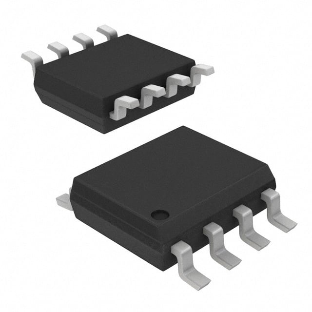
ICGOO电子元器件商城为您提供ICL7665SCBAZ由Intersil设计生产,在icgoo商城现货销售,并且可以通过原厂、代理商等渠道进行代购。 ICL7665SCBAZ价格参考¥18.35-¥36.57。IntersilICL7665SCBAZ封装/规格:PMIC - 监控器, 开路漏极或开路集电极 监控器 2 通道 8-SOIC。您可以下载ICL7665SCBAZ参考资料、Datasheet数据手册功能说明书,资料中有ICL7665SCBAZ 详细功能的应用电路图电压和使用方法及教程。
| 参数 | 数值 |
| 产品目录 | 集成电路 (IC)半导体 |
| 描述 | IC VOLT DETECTOR OVER/UND 8-SOIC监控电路 CMOS OVER/UNDERV DETCETOR 8 COM |
| 产品分类 | |
| 品牌 | Intersil |
| 产品手册 | |
| 产品图片 |
|
| rohs | 符合RoHS无铅 / 符合限制有害物质指令(RoHS)规范要求 |
| 产品系列 | 电源管理 IC,监控电路,Intersil ICL7665SCBAZ- |
| NumberofInputsMonitored | 2 Input |
| 数据手册 | |
| 产品型号 | ICL7665SCBAZ |
| PCN组件/产地 | |
| 产品种类 | 监控电路 |
| 人工复位 | No Manual Reset |
| 供应商器件封装 | 8-SOIC |
| 准确性 | 2 % |
| 包装 | 管件 |
| 受监控电压数 | 2 |
| 商标 | Intersil |
| 复位 | 高有效 |
| 复位超时 | - |
| 安装类型 | 表面贴装 |
| 安装风格 | SMD/SMT |
| 封装 | Tube |
| 封装/外壳 | 8-SOIC(0.154",3.90mm 宽) |
| 封装/箱体 | SOIC-8 |
| 工作温度 | 0°C ~ 70°C |
| 工作电源电流 | 2.9 uA |
| 工厂包装数量 | 98 |
| 最大工作温度 | + 70 C |
| 最小工作温度 | 0 C |
| 标准包装 | 98 |
| 欠电压阈值 | 1.2 V |
| 电压-阈值 | 可调节/可选择 |
| 电池备用开关 | No Backup |
| 电源电压-最大 | 16 V |
| 电源电压-最小 | 1.6 V |
| 监视器 | No Watchdog |
| 类型 | Voltage Monitors |
| 系列 | ICL7665 |
| 被监测输入数 | 2 Input |
| 输出 | 开路漏极或开路集电极 |
| 输出类型 | Open Collector / Drain |
| 过电压阈值 | 1.4 V |
| 阈值电压 | 1.3 V |





- 商务部:美国ITC正式对集成电路等产品启动337调查
- 曝三星4nm工艺存在良率问题 高通将骁龙8 Gen1或转产台积电
- 太阳诱电将投资9.5亿元在常州建新厂生产MLCC 预计2023年完工
- 英特尔发布欧洲新工厂建设计划 深化IDM 2.0 战略
- 台积电先进制程称霸业界 有大客户加持明年业绩稳了
- 达到5530亿美元!SIA预计今年全球半导体销售额将创下新高
- 英特尔拟将自动驾驶子公司Mobileye上市 估值或超500亿美元
- 三星加码芯片和SET,合并消费电子和移动部门,撤换高东真等 CEO
- 三星电子宣布重大人事变动 还合并消费电子和移动部门
- 海关总署:前11个月进口集成电路产品价值2.52万亿元 增长14.8%


PDF Datasheet 数据手册内容提取
DATASHEET ICL7665S FN3182 CMOS Micropower Over/Under Voltage Detector Rev 10.00 August 10, 2015 The ICL7665S super CMOS micropower Over/Under Features voltage detector contains two low power, individually • Guaranteed 10µA maximum quiescent current programmable voltage detectors on a single CMOS chip. over-temperature Requiring typically 3A for operation, the device is intended for battery-operated systems and instruments which require • Guaranteed wider operating voltage range over entire high or low voltage warnings, settable trip points, or fault operating temperature range monitoring and correction. The trip points and hysteresis of • 2% threshold accuracy (ICL7665SA) the two voltage detectors are individually programmed via external resistors. An internal bandgap type reference • Dual comparator with precision internal reference provides an accurate threshold voltage while operating from • 100ppm/°C temperature coefficient of threshold voltage any supply in the 1.6V to 16V range. • 100% tested at 2V The ICL7665S, super programmable Over/Under voltage • Output current sinking ability . . . . . . . . . . . . . Up to 20mA detector is a direct replacement for the industry standard. The ICL7665B offering wider operating voltage and • Individually programmable upper and lower trip voltages temperature ranges, improved threshold accuracy and hysteresis levels (ICL7665SA), and temperature coefficient, and guaranteed • Pb-Free available (RoHS Compliant) maximum supply current. All improvements are highlighted in the electrical characteristics section. All critical Applications parameters are guaranteed over the entire commercial • Pocket pagers and industrial temperature ranges. • Portable instrumentation Pinout • Charging systems ICL7665S (SOIC, PDIP) • Memory power back-up TOP VIEW • Battery operated systems OUT 1 1 8 V+ • Portable computers HYST 1 2 7 OUT 2 • Level detectors SET 1 3 6 SET 2 GND 4 5 HYST 2 FN3182 Rev 10.00 Page 1 of 15 August 10, 2015
ICL7665S Ordering Information TEMP. PKG. PART NUMBER PART MARKING RANGE (°C) PACKAGE DWG. # ICL7665SACBAZ (Notes 1, 3) 7665S ACBAZ 0 to +70 8 Ld SOIC (Pb-free) M8.15 ICL7665SACBAZA (Notes 1, 3) 7665S ACBAZ 0 to +70 8 Ld SOIC (Pb-free) M8.15 ICL7665SACPAZ (Note 2) 7665S ACPAZ 0 to +70 8 Ld PDIP (Pb-free) E8.3 ICL7665SAIBAZA (Notes 1, 3) 7665 SAIBAZ -40 to +85 8 Ld SOIC (Pb-free) M8.15 ICL7665SAIPAZ (Note 2) 7665S AIPAZ -40 to +85 8 Ld PDIP (Pb-free) E8.3 ICL7665SCBAZ (Notes 1, 3) 7665 SCBAZ 0 to +70 8 Ld SOIC (Pb-free) M8.15 ICL7665SCBAZA (Notes 1, 3) 7665 SCBAZ 0 to +70 8 Ld SOIC (Pb-free) M8.15 ICL7665SCPAZ (Note 2) 7665S CPAZ 0 to +70 8 Ld PDIP (Pb-free) E8.3 ICL7665SIBAZ (Notes 1, 3) 7665 SIBAZ -40 to +85 8 Ld SOIC (Pb-free) M8.15 ICL7665SIBAZA (Notes 1, 3) 7665 SIBAZ -40 to +85 8 Ld SOIC(Pb-free) M8.15 NOTES: 1. Add “-T*” suffix for tape and reel. Please refer to TB347 for details on reel specifications. 2. Pb-free PDIPs can be used for through hole wave solder processing only. They are not intended for use in Reflow solder processing applications. 3. Intersil Pb-free plus anneal products employ special Pb-free material sets; molding compounds/die attach materials and 100% matte tin plate termination finish, which are RoHS compliant and compatible with both SnPb and Pb-free soldering operations. Intersil Pb-free products are MSL classified at Pb-free peak reflow temperatures that meet or exceed the Pb-free requirements of IPC/JEDEC J STD-020. FN3182 Rev 10.00 Page 2 of 15 August 10, 2015
ICL7665S Absolute Maximum Ratings Thermal Information Supply Voltage (Note 5). . . . . . . . . . . . . . . . . . . . . . . . .-0.3 to +18V Thermal Resistance (Typical, Note 4) JA (°C/W) Output Voltages OUT1 and OUT2. . . . . . . . . . . . . . . .-0.3V to +18V PDIP Package* . . . . . . . . . . . . . . . . . . . . . . . . . . . . 115 (with respect to GND) (Note 5) SOIC Package. . . . . . . . . . . . . . . . . . . . . . . . . . . . . 160 Output Voltages HYST1 and HYST2. . . . . . . . . . . . . .-0.3V to +18V Maximum Junction Temperature (Plastic) . . . . . . . . . . . . . . .+150°C (with respect to V+) (Note 5) Maximum Junction Temperature (CERDIP). . . . . . . . . . . . . .+175°C Input Voltages SET1 and SET2. . . . . (GND -0.3V) to (V+ V- +0.3V) Maximum Storage Temperature Range. . . . . . . . . .-65°C to +150°C (Note 5) Maximum Lead Temperature (Soldering 10s) . . . . . . . . . . . .+300°C Maximum Sink Output OUT1 and OUT2. . . . . . . . . . . . . . . . . 25mA (SOIC - Lead Tips Only) Maximum Source Output Current Pb-Free Reflow Profile. . . . . . . . . . . . . . . . . . . . . . . . .see link below HYST1 and HYST2 . . . . . . . . . . . . . . . . . . . . . . . . . . . . . . -25mA http://www.intersil.com/pbfree/Pb-FreeReflow.asp Operating Conditions *Pb-free PDIPs can be used for through hole wave solder processing only. They are not intended for use in Reflow solder processing Temperature Range applications. ICL7665SC. . . . . . . . . . . . . . . . . . . . . . . . . . . . . . . . 0°C to +70°C ICL7665SI . . . . . . . . . . . . . . . . . . . . . . . . . . . . . . .-40°C to +85°C CAUTION: Do not operate at or near the maximum ratings listed for extended periods of time. Exposure to such conditions may adversely impact product reliability and result in failures not covered by warranty. NOTES: 4. JA is measured with the component mounted on an evaluation PC board in free air. 5. Due to the SCR structure inherent in the CMOS process used to fabricate these devices, connecting any terminal to voltages greater than (V+ +0.3V) or less than (GND - 0.3V) may cause destructive device latchup. For these reasons, it is recommended that no inputs from external sources not operating from the same power supply be applied to the device before its supply is established, and that in multiple supply systems, the supply to the ICL7665S be turned on first. If this is not possible, current into inputs and/or outputs must be limited to 0.5mA and voltages must not exceed those defined above. Electrical Specifications The specifications below are applicable to both the ICL7665S and ICL7665SA. V+ = 5V, TA = +25°C, Test Circuit Figure 7. Unless Otherwise Specified PARAMETER SYMBOL TEST CONDITIONS MIN TYP MAX UNITS Operating Supply Voltage V+ ICL7665S TA = +25°C 1.6 - 16 V 0°C TA +70°C 1.8 - 16 V -25°C TA +85°C 1.8 - 16 V ICL7665SA 0°C TA +70°C 1.8 - 16 V -25°C TA +85°C 1.8 - 16 V Supply Current I+ GND VSET1, VSET2 V+, All Outputs Open Circuit 0°C TA +70°C V+ = 2V - 2.5 10 µA V+ = 9V - 2.6 10 µA V+ = 15V - 2.9 10 µA -40°C TA +85°C V+ = 2V - 2.5 10 µA V+ = 9V - 2.6 10 µA V+ = 15V - 2.9 10 µA Input Trip Voltage VSET1 ICL7665S 1.20 1.30 1.40 V VSET2 1.20 1.30 1.40 V VSET1 ICL7665SA 1.275 1.30 1.325 V VSET2 1.275 1.30 1.325 V Temperature Coefficient of VSET ICL7665S - 200 - ppm VSET T ICL7665SA - 100 - ppm Supply Voltage Sensitivity of VSET ROUT1, ROUT2, RHYST1, R2HYST2 = 1M - 0.03 - %/V VSET1, VSET2 VS 2V V+ 10V FN3182 Rev 10.00 Page 3 of 15 August 10, 2015
ICL7665S Electrical Specifications The specifications below are applicable to both the ICL7665S and ICL7665SA. V+ = 5V, TA = +25°C, Test Circuit Figure 7. Unless Otherwise Specified (Continued) PARAMETER SYMBOL TEST CONDITIONS MIN TYP MAX UNITS Output Leakage Currents of IOLK VSET = 0V or VSET 2V - 10 200 nA OUT and HYST IHLK - -10 -100 nA IOLK V+ = 15V - - 2000 nA IHLK - - -500 nA Output Saturation Voltages VOUT1 VSET1 = 2V, V+ = 2V - 0.2 0.5 V IOUT1 = 2mA V+ = 5V - 0.1 0.3 V V+ = 15V - 0.06 0.2 V Output Saturation Voltages VHYST1 VSET1 = 2V, V+ = 2V - -0.15 -0.30 V IHYST1 = -0.5mA V+ = 5V - -0.05 -0.15 V V+ = 15V - -0.02 -0.10 V Output Saturation Voltages VOUT2 VSET2 = 0V, V+ = 2V - 0.2 0.5 V IOUT2 = 2mA V+ = 5V - 0.15 0.3 V V+ = 15V - 0.11 0.25 V Output Saturation Voltages VHYST2 VSET2 = 2V V+ = 2V, IHYST2 = -0.2mA - -0.25 -0.8 V V+ = 5V, IHYST2 = -0.5mA - -0.43 -1.0 V V+ = 15V, IHYST2 = -0.5mA - -0.35 -0.8 V VSET Input Leakage Current ISET GND VSET V+ - 0.01 10 nA Input for Complete Output VSET ROUT = 4.7k, ICL7665S - 1.0 - mV Change RHYST = 20k, ICL7665SA - 0.1 - mV VOUTLO = 1% V+, VOUTHI = 99% V+ Difference in Trip Voltages VSET1 - ROUT, RHYST = 1mW - 5 50 mV VSET2 Output/Hysteresis ROUT, RHYST = 1mW ICL7665S - 1 - mV Difference ICL7665SA - 0.1 - mV NOTES: 6. Derate above +25°C ambient temperature at 4mW/°C. 7. All significant improvements over the industry standard ICL7665 are highlighted. FN3182 Rev 10.00 Page 4 of 15 August 10, 2015
ICL7665S AC Electrical Specifications PARAMETER SYMBOL TEST CONDITIONS MIN TYP MAX UNITS OUTPUT DELAY TIMES Input Going HI tSO1D VSET Switched between 1.0V to 1.6V - 85 - µs ROUT = 4.7k, CL = 12pF tSH1D RHYST = 20k, CL = 12pF - 90 - µs tSO2D - 55 - µs tSH2D - 55 - µs Input Going LO tSO1D VSET Switched between 1.6V to 1.0V - 75 - µs ROUT = 4.7k, CL = 12pF tSH1D RHYST = 20k, CL = 12pF - 80 - µs tSO2D - 60 - µs tSH2D - 60 - µs Output Rise Times tO1R VSET Switched between 1.0V to 1.6V - 0.6 - µs ROUT = 4.7k, CL = 12pF tO2R RHYST = 20k, CL = 12pF - 0.8 - µs tH1R - 7.5 - µs tH2R - 0.7 - µs Output Fall Times tO1F VSET Switched between 1.0V to 1.6V - 0.6 - µs ROUT = 4.7k, CL = 12pF tO2F RHYST = 20k, CL = 12pF - 0.7 - µs tH1F - 4.0 - µs tH2F - 1.8 - µs Functional Block Diagram V+ HYST2 SET1 - + HYST1 REF + OUT2 SET2 - OUT1 GND CONDITIONS (Note 5) VSET1 > 1.3V, OUT1 Switch ON, HYST1 Switch ON VSET1 < 1.3V, OUT1 Switch OFF, HYST1 Switch OFF VSET2 > 1.3V, OUT2 Switch OFF, HYST2 Switch ON VSET2 < 1.3V, OUT2 Switch ON, HYST2 Switch OFF NOTE: 8. See Electrical Specifications for exact thresholds. FN3182 Rev 10.00 Page 5 of 15 August 10, 2015
ICL7665S Typical Performance Curves 2.0 2.0 V+ = 2V V+ = 2V V) V) N ( 1.5 N ( 1.5 O O TI V+ = 5V TI A A R R U U AT 1.0 V+ = 9V AT 1.0 E S E S V+ = 5V G G V+ = 9V A A T T OL 0.5 OL 0.5 V V+ = 15V V V+ = 15V 0 0 0 5 10 15 20 0 5 10 15 20 IOUTOUT1 (mA) IOUTOUT2 (mA) FIGURE 1. OUT1 SATURATION VOLTAGE AS A FUNCTION FIGURE 2. OUT2 SATURATION VOLTAGE AS A FUNCTION OF OUTPUT CURRENT OF OUTPUT CURRENT -20 -16 -12 -8 -4 0 -5.0 -4.0 -3.0 -2.0 -1.0 0 0 V) 0 V) TA = 25°C E ( TA = 25°C E ( G G A A -0.4 LT -1.0 LT V+ = 15V O O V V N V+ = 15V N O O -0.8 ATI -2.0 ATI UR V+ = 9V UR AT AT V+ = 9V -1.2 S -3.0 S T T U U P P T T -1.6 OU -4.0 OU T1 T2 V+ = 5V V+ = 2V YS V+ = 5V V+ = 2V YS -2.0 H -5.0 H HYST1 OUTPUT CURRENT (mA) HYST2 OUTPUT CURRENT (mA) FIGURE 3. HYST1 OUTPUT SATURATION VOLTAGE vs FIGURE 4. HYST2 OUTPUT SATURATION VOLTAGE vs HYST1 OUTPUT CURRENT HYST2 OUTPUT CURRENT 5.0 5.0 4.5 0V VSET1, VSET2 V+ 4.5 0V VSET1, VSET2 V+ SUPPLY CURRENT (A) 433221......050505 VV++ == 12V5V V+ = 9V SUPPLY CURRENT (A) 433221......050505 TA =TA 2T 5A=° -C=2 07°0C°C 1.0 1.0 0.5 0.5 0 0 -25 0 +20 +40 +60 0 2 4 6 8 10 12 14 16 AMBIENT TEMPERATURE (°C) SUPPLY VOLTAGE (V+) FIGURE 5. SUPPLY CURRENT AS A FUNCTION OF AMBIENT FIGURE 6. SUPPLY CURRENT AS A FUNCTION OF SUPPLY TEMPERATURE VOLTAGE FN3182 Rev 10.00 Page 6 of 15 August 10, 2015
ICL7665S Detailed Description If the SET voltages must be applied before the supply voltage V+, the input current should be limited to less than 0.5mA by As shown in the Functional Diagram, the ICL7665S consists appropriate external resistors, usually required for voltage of two comparators which compare input voltages on the setting anyway. A similar precaution should be taken with the SET1 and SET2 terminals to an internal 1.3V bandgap outputs if it is likely that they will be driven by other circuits to reference. The outputs from the two comparators drive levels outside the supplies at any time. open-drain N-channel transistors for OUT1 and OUT2, and Additionally, with a V+ supply that has ringing or drooping after open-drain P-channel transistors for HYST1 and HYST2 power up, a false transition on the OUTx output may occur outputs. Each section, the Undervoltage Detector and the even though the resistor programmed threshold voltage is not Overvoltage Detector, is independent of the other, although encroached upon. This occurs as the internal bandgap circuit both use the internal 1.3V reference. The offset voltages of time constant, on the order of a microsecond is matched by the the two comparators will normally be unequal so VSET1 will V+ transient. If this occurs connecting a 1F to the SETx pin will generally not quite equal VSET2. eliminate the OUTx false transition as the additional The input impedance of the SET1 and SET2 pins are capacitance moves the external time constant three orders of extremely high, and for most practical applications can be magnitude above the internal time constant. ignored. The four outputs are open-drain MOS transistors, and when ON behave as low resistance switches to their respective supply rails. This minimizes errors in setting up VSET1, 1.6V VSET2 the hysteresis, and maximizes the output flexibility. The INPUT 1.0V operating currents of the bandgap reference and the tSO1D tO1R comparators are around 100nA each. tO1F tSO1D V+ OUT1 (5V) V+ GND tSH1D tH1F 4.7k OUT1 tH1R V(5+V) HYST1 tSH1D GND HYST1 tSO2D tSO2D 1 OUT1 V+ 8 4k.7 tO2R tO2F V(5+V) OUT2 OUT2 GND 2 HYST1OUT2 7 INPUT 3 SET1 SET2 6 tSH2D tSH2D HYST2 tH2R tH2F V+ 4 GNDHYST2 5 (5V) HYST2 GND 20 20 12 12 12 12 FIGURE 8. SWITCHING WAVEFORMS k k pF pF pF pF Simple Threshold Detector 1.6V 1.0V Figure 9 shows the simplest connection of the ICL7665S for FIGURE 7. TEST CIRCUITS threshold detection. From the graph 9B, it can be seen that at low input voltage OUT1 is OFF, or high, while OUT2 is Precautions ON, or low. As the input rises (e.g., at power-on) toward VNOM (usually the eventual operating voltage), OUT2 goes Junction isolated CMOS devices like the ICL7665S have an high on reaching VTR2. If the voltage rises above VNOM as inherent SCR or 4-layer PNPN structure distributed throughout much as VTR1, OUT1 goes low. The Equations are giving the die. Under certain circumstances, this can be triggered into VSET1 and VSET2 are from Figure 9A: a potentially destructive high current mode. This latchup can be R R triggered by forward-biasing an input or output with respect to V = V ----------------1---1------------- V = V ----------------1---2------------- SET1 INR +R SET2 INR +R the power supply, or by applying excessive supply voltages. In 11 21 12 22 very low current analog circuits, such as the ICL7665S, this Since the voltage to trip each comparator is nominally 1.3V, SCR can also be triggered by applying the input power supply extremely rapidly (“instantaneously”), e.g., through a low the value VIN for each trip point can be found from impedance battery and an ON/OFF switch with short lead R11+R21 R11+R21 V = V ----------------------------------=1.3---------------------------------- for detector 1 lengths. The rate-of-rise of the supply voltage can exceed TR1 SET1 R11 R11 100V/s in such a circuit. A low impedance capacitor (e.g., 0.05F disc ceramic) between the V+ and GND pins of the and ICL7665S can be used to reduce the rate-of-rise of the supply R +R R +R 12 22 12 22 V = V ----------------------------------=1.3---------------------------------- for detector 2 voltage in battery applications. In line operated systems, the TR2 SET2 R R 12 12 rate-of-rise of the supply is limited by other considerations, and is normally not a problem. FN3182 Rev 10.00 Page 7 of 15 August 10, 2015
ICL7665S VIN VOUT OFF RP2 RP1 V+ R21 OUT1 OUT2 R22 SET1 SET2 R11 R12 ON VTR2 VNOM VTR1 DETECTOR 2 DETECTOR 1 FIGURE 9A. CIRCUIT CONFIGURATION FIGURE 9B. TRANSFER CHARACTERISTICS FIGURE 9. SIMPLE THRESHOLD DETECTOR VIN OUT ON R31 R32 V+ HYST1 HYST2 R21 R22 SET1 SET2 VL2 VU2 VL1 VU1 OUT1 OUT2 OFF VIN OVERVOLTAGE OVERVOLTAGE VNOM R11 R12 DETECTOR 2 DETECTOR 1 FIGURE 10A. CIRCUIT CONFIGURATION FIGURE 10B. TRANSFER CHARACTERISTICS FIGURE 10. THRESHOLD DETECTOR WITH HYSTERESIS Either detector may be used alone, as well as both together, becomes controlled by only R1N and R2N, a lower value. in any of the circuits shown here. The input will then have to fall to this new point to restore the initial comparator state, but as soon as this occurs, the trip When VIN is very close to one of the trip voltage, normal point will be raised again. variations and noise may cause it to wander back and forth across this level, leading to erratic output ON and OFF An alternative circuit for obtaining hysteresis is shown in conditions. The addition of hysteresis, making the trip points Figure 11. In this configuration, the HYST pins put the extra slightly different for rising and falling inputs, will avoid this resistor in parallel with the upper setting resistor. The values condition. of the resistors differ, but the action is essentially the same. The governing Equations are given in Table 1. These ignore Threshold Detector with Hysteresis the effects of the resistance of the HYST outputs, but these Figure 10A shows how to set up such hysteresis, while can normally be neglected if the resistor values are above Figure 10B shows how the hysteresis around each trip point about 100k. produces switching action at different points depending on R +R R +R 12 22 12 22 V = V ----------------------------------=1.3---------------------------------- for detector 2 whether VIN is rising or falling (the arrows indicated direction TR2 SET2 R12 R12 of change. The HYST outputs are basically switches which short out R31 or R32 when VIN is above the respective trip point. Thus if the input voltage rises from a low value, the trip point will be controlled by R1N, R2N, and R3N, until the trip point is reached. As this value is passed, the detector changes state, R3N is shorted out, and the trip point FN3182 Rev 10.00 Page 8 of 15 August 10, 2015
ICL7665S Applications VIN Single Supply Fault Monitor Figure 12 shows an over/under voltage fault monitor for a RP RP V+ single supply. The overvoltage trip point is centered around R21 OUT1 OUT2 R22 5.5V and the undervoltage trip point is centered around 4.5V. R31 R32 Both have some hysteresis to prevent erratic output ON and HYST1 HYST2 OFF conditions. The two outputs are connected in a wired OR configuration with a pull-up resistor to generate a power SET1 SET2 OK signal. R11 R12 +5V SUPPLY FIGURE 11. AN ALTERNATIVE HYSTERESIS CIRCUIT R21 324k V+ 249k R22 HYST1 HYST2 TABLE 1. SET-POINT EQUATIONS 13M5% R31 R32 75%.5M NO HYSTERESIS VSET1 VSET2 Overvoltage VTRIP = R11 + R21 x VSET1 100k R11 R12 100k R11 OUT1 OUT2 OPEN VOLTAGE DETECTOR Overvoltage VTRIP = R12R +1 2R22 x VSET2 ODEPTEENC VTOOLRTAGE V+ VVUL == 44..4555VV HYSTERESIS PER FIGURE 10A VU = 5.55V 1M VL = 5.45V POWER R11 + R21 + R31 OK VU1 = x VSET1 R11 FIGURE 12. FAULT MONITOR FOR A SINGLE SUPPLY Overvoltage VTRIP VL1 = R11 + R21 x VSET1 Multiple Supply Fault Monitor R11 The ICL7665S can simultaneously monitor several supplies R12 + R22 + R32 VU2 = x VSET2 when connected as shown in Figure 13. The resistors are R12 chosen such that the sum of the currents through R21A, Undervoltage VTRIP R21B, and R31 is equal to the current through R11 when the two input voltage are at the desired low voltage detection R12 + R22 VL2 = R12 x VSET2 point. The current through R11 at this point is equal to 1.3V/R11. The voltage at the VSET input depends on the HYSTERESIS PER FIGURE 11 voltage of both supplies being monitored. The trip voltage of R11 + R21 one supply while the other supply is at the nominal voltage VU1 = x VSET1 R11 will be different that the trip voltage when both supplies are below their nominal voltages. Overvoltage VTRIP R21R31 The other side of the ICL7665S can be used to detect the R11 + absence of negative supplies. The trip points for OUT1 VL1 = R21 + R31 x VSET1 depend on both the negative supply voltages and the actual R11 voltage of the +5V supply. R12 + R22 VU2 = x VSET2 R12 Overvoltage VTRIP R22R32 R12 + VL2 = R22 + R32 x VSET2 R12 FN3182 Rev 10.00 Page 9 of 15 August 10, 2015
ICL7665S As long as VSET1 is greater than 1.3V, OUT1 is low, but +5V 274k when VSET1 drops below 1.3V, OUT1 goes high shutting off R21A V+ the ICL7663S. The OUT2 is used for low battery warning. +5V HYST1 HYST2 When VSET2 is greater than 1.3V, OUT2 is high and the low 100k 22M R21 M22 bisa ltotewr ya wnda rtnhien glo iws obna.t tWerhye wna VrnSiEnTg2 g doreosp so fbf.e Tlohwe 1tr.i3pV v, oOltUagTe2 VSET1 VSET2 for low battery warning can be set higher than the trip 49.9k 301 787 +15V R11 OUT1 OUT2 k k +5V voltage for shutdown to give advance low battery warning before the battery is disconnected. 1.02M R21B -5V -15V 1M Power Fail Warning and Power-up/Power-down Reset POWER Figure 14 shows a power fail warning circuit with OK power-up/power-down reset. When the unregulated DC FIGURE 13. MULTIPLE SUPPLY FAULT MONITOR input is above the trip point, OUT1 is low. When the DC input drops below the trip point, OUT1 shuts OFF and the power Combination Low Battery Warning and Low fail warning goes high. The voltage on the input of the 7805 Battery Disconnect will continue to provide 5V out at 1A until VIN is less than When using rechargeable batteries in a system, it is 7.3V, this circuit will provide a certain amount of warning important to keep the batteries from being over discharged. before the 5V output begins to drop. The circuit shown in Figure 14 provides a low battery The ICL7665S OUT2 is used to prevent a microprocessor warning and also disconnects the low battery from the rest of from writing spurious data to a CMOS battery backup the system to prevent damage to the battery. The OUT1 is memory by causing OUT2 to go low when the 7805 5V used to shutdown the ICL7663S when the battery voltage output drops below the ICL7665S trip point. drops to the value where the load should be disconnected. +5V 100 1A R31 R32 V+ 1M HYST1 HYST2 V+ OUT1 OUT2 + R21 ICL7665S R22 ICL7663S SENSE SET1 SET2 V+ - SHUTDOWN VSET GND R11 R12 OUT1 GND OUT2 1M LOW BATTERY SHUTDOWN LOW BATTERY WARNING FIGURE 14. LOW BATTERY WARNING AND LOW BATTERY DISCONNECT FN3182 Rev 10.00 Page 10 of 15 August 10, 2015
ICL7665S UNREGULATED 7805 DC INPUT 5V REGULATOR 4700F 470F BACKUP BATTERY V+ HYST1 HYST2 5.86k 22M ICL7665S VSET1 VSET2 715k 2.2M 130k OUT1 OUT2 1M 1M RESET OR WRITE ENABLE 1M POWER FAIL WARNING FIGURE 15. POWER FAIL WARNING AND POWERUP/POWERDOWN RESET Simple High/Low Temperature Alarm AC Power Fail and Brownout Detector Figure 16 illustrates a simple high/low temperature alarm Figure 17 shows a circuit that detects AC undervoltage by which uses the ICL7665S with an NPN transistor. The voltage monitoring the secondary side of the transformer. The at the top of R1 is determined by the VBE of the transistor and capacitor, C1, is charged through R1 when OUT1 is OFF. With the position of R1’s wiper arm. This voltage has a negative a normal 100 VAC input to the transformer, OUT1 will temperature coefficient. R1 is adjusted so that VSET2 equals discharge C1 once every cycle, approximately every 16.7ms. 1.3V when the NPN transistor’s temperature reaches the When the AC input voltage is reduced, OUT1 will stay OFF, so temperature selected for the high temperature alarm. When that C1 does not discharge. When the voltage on C1 reaches this occurs, OUT2 goes low. R2 is adjusted so that VSET1 1.3V, OUT2 turns OFF and the power fail warning goes high. equals 1.3V when the NPN transistor’s temperature reaches The time constant, R1C1, is chosen such that it takes longer the temperature selected for the low temperature alarm. When than 16.7ms to charge C1 1.3V. the temperature drops below this limit, OUT1 goes low. FN3182 Rev 10.00 Page 11 of 15 August 10, 2015
ICL7665S + - 5V 470k LOW TEMPERATURE TEMPERATURE R3 V+ LIMIT ADJUST SENSOR HYST1 HYST2 (GENERAL PURPOSE NPN TRANSISTOR) 22k R4 ICL7665S R6 22M 27k R2 VSET1 VSET2 R5 1M OUT1 OUT2 R7 1.5M R1 10k HIGH V+ TEMPERATURE ALARM SIGNAL LIMIT ADJUST 1M FOR DRIVING LEDS, BELLS, ETC. FIGURE 16. SIMPLE HIGH/LOW TEMPERATURE ALARM 7805 5V REGULATOR 20V 4700µF 5V, 1A CENTERED 110VAC TAPPED 60Hz TRANS. +5V 601k HYST1 HYST2 R1 ICL7665S 1M VSET1 VSET2 100k POWER FAIL 1M OUT1 OUT2 WARNING 1M C1 FIGURE 17. AC POWER FAIL AND BROWNOUT DETECTOR FN3182 Rev 10.00 Page 12 of 15 August 10, 2015
ICL7665S Revision History The revision history provided is for informational purposes only and is believed to be accurate, but not warranted. Please go to the web to make sure that you have the latest revision. DATE REVISION CHANGE August 10, 2015 FN3182.10 Added Rev History beginning with Rev 10. Added About Intersil Verbiage. Updated Ordering Information Table on page2. About Intersil Intersil Corporation is a leading provider of innovative power management and precision analog solutions. The company's products address some of the largest markets within the industrial and infrastructure, mobile computing and high-end consumer markets. For the most updated datasheet, application notes, related documentation and related parts, please see the respective product information page found at www.intersil.com. You may report errors or suggestions for improving this datasheet by visiting www.intersil.com/ask. Reliability reports are also available from our website at www.intersil.com/support. © Copyright Intersil Americas LLC 2004-2015. All Rights Reserved. All trademarks and registered trademarks are the property of their respective owners. For additional products, see www.intersil.com/en/products.html Intersil products are manufactured, assembled and tested utilizing ISO9001 quality systems as noted in the quality certifications found at www.intersil.com/en/support/qualandreliability.html Intersil products are sold by description only. Intersil may modify the circuit design and/or specifications of products at any time without notice, provided that such modification does not, in Intersil's sole judgment, affect the form, fit or function of the product. Accordingly, the reader is cautioned to verify that datasheets are current before placing orders. Information furnished by Intersil is believed to be accurate and reliable. However, no responsibility is assumed by Intersil or its subsidiaries for its use; nor for any infringements of patents or other rights of third parties which may result from its use. No license is granted by implication or otherwise under any patent or patent rights of Intersil or its subsidiaries. For information regarding Intersil Corporation and its products, see www.intersil.com FN3182 Rev 10.00 Page 13 of 15 August 10, 2015
ICL7665S Dual-In-Line Plastic Packages (PDIP) E8.3 (JEDEC MS-001-BA ISSUE D) N 8 LEAD DUAL-IN-LINE PLASTIC PACKAGE E1 INDEX INCHES MILLIMETERS AREA 1 2 3 N/2 SYMBOL MIN MAX MIN MAX NOTES -B- A - 0.210 - 5.33 4 -A- D E A1 0.015 - 0.39 - 4 BASE A2 0.115 0.195 2.93 4.95 - PLANE A2 -C- A B 0.014 0.022 0.356 0.558 - SEATING PLANE L CL B1 0.045 0.070 1.15 1.77 8, 10 D1 D1 A1 eA C 0.008 0.014 0.204 0.355 - B1 e eC C D 0.355 0.400 9.01 10.16 5 B eB D1 0.005 - 0.13 - 5 0.010 (0.25) M C A B S E 0.300 0.325 7.62 8.25 6 NOTES: E1 0.240 0.280 6.10 7.11 5 1. Controlling Dimensions: INCH. In case of conflict between e 0.100 BSC 2.54 BSC - English and Metric dimensions, the inch dimensions control. 2. Dimensioning and tolerancing per ANSI Y14.5M-1982. eA 0.300 BSC 7.62 BSC 6 3. Symbols are defined in the “MO Series Symbol List” in Section eB - 0.430 - 10.92 7 2.2 of Publication No. 95. L 0.115 0.150 2.93 3.81 4 4. Dimensions A, A1 and L are measured with the package seated N 8 8 9 in JEDEC seating plane gauge GS-3. Rev. 0 12/93 5. D, D1, and E1 dimensions do not include mold flash or protru- sions. Mold flash or protrusions shall not exceed 0.010 inch (0.25mm). 6. E and eA are measured with the leads constrained to be per- pendicular to datum -C- . 7. eB and eC are measured at the lead tips with the leads uncon- strained. eC must be zero or greater. 8. B1 maximum dimensions do not include dambar protrusions. Dambar protrusions shall not exceed 0.010 inch (0.25mm). 9. N is the maximum number of terminal positions. 10. Corner leads (1, N, N/2 and N/2 + 1) for E8.3, E16.3, E18.3, E28.3, E42.6 will have a B1 dimension of 0.030 - 0.045 inch (0.76 - 1.14mm). FN3182 Rev 10.00 Page 14 of 15 August 10, 2015
ICL7665S Package Outline Drawing M8.15 8 LEAD NARROW BODY SMALL OUTLINE PLASTIC PACKAGE Rev 4, 1/12 DETAIL "A" 1.27 (0.050) 0.40 (0.016) INDEX 6.20 (0.244) AREA 5.80 (0.228) 0.50 (0.20) x 45° 4.00 (0.157) 0.25 (0.01) 3.80 (0.150) 8° 1 2 3 0° 0.25 (0.010) 0.19 (0.008) TOP VIEW SIDE VIEW “B” 2.20 (0.087) 1 8 SEATING PLANE 0.60 (0.023) 5.00 (0.197) 1.75 (0.069) 2 7 4.80 (0.189) 1.35 (0.053) 1.27 (0.050) 3 6 -C- 4 5 1.27 (0.050) 0.25(0.010) 0.10(0.004) 0.51(0.020) 5.20(0.205) 0.33(0.013) SIDE VIEW “A TYPICAL RECOMMENDED LAND PATTERN NOTES: 1. Dimensioning and tolerancing per ANSI Y14.5M-1994. 2. Package length does not include mold flash, protrusions or gate burrs. Mold flash, protrusion and gate burrs shall not exceed 0.15mm (0.006 inch) per side. 3. Package width does not include interlead flash or protrusions. Interlead flash and protrusions shall not exceed 0.25mm (0.010 inch) per side. 4. The chamfer on the body is optional. If it is not present, a visual index feature must be located within the crosshatched area. 5. Terminal numbers are shown for reference only. 6. The lead width as measured 0.36mm (0.014 inch) or greater above the seating plane, shall not exceed a maximum value of 0.61mm (0.024 inch). 7. Controlling dimension: MILLIMETER. Converted inch dimensions are not necessarily exact. 8. This outline conforms to JEDEC publication MS-012-AA ISSUE C. FN3182 Rev 10.00 Page 15 of 15 August 10, 2015

 Datasheet下载
