ICGOO在线商城 > ICL3225CAZ

 Datasheet下载
- 型号: ICL3225CAZ
- 制造商: Intersil
- 库位|库存: xxxx|xxxx
- 要求:
| 数量阶梯 | 香港交货 | 国内含税 |
| +xxxx | $xxxx | ¥xxxx |
查看当月历史价格
查看今年历史价格
ICL3225CAZ产品简介:
ICGOO电子元器件商城为您提供ICL3225CAZ由Intersil设计生产,在icgoo商城现货销售,并且可以通过原厂、代理商等渠道进行代购。 提供ICL3225CAZ价格参考以及IntersilICL3225CAZ封装/规格参数等产品信息。 你可以下载ICL3225CAZ参考资料、Datasheet数据手册功能说明书, 资料中有ICL3225CAZ详细功能的应用电路图电压和使用方法及教程。
| 参数 | 数值 |
| 产品目录 | 集成电路 (IC) |
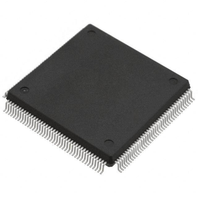
| 描述 | IC 2DRVR/2RCVR RS232 3V 20-SSOP |
| 产品分类 | |
| 品牌 | Intersil |
| 数据手册 | |
| 产品图片 |
|
| 产品型号 | ICL3225CAZ |
| rohs | 无铅 / 符合限制有害物质指令(RoHS)规范要求 |
| 产品系列 | - |
| 供应商器件封装 | 20-SSOP |
| 包装 | 管件 |
| 协议 | RS232 |
| 双工 | 全 |
| 安装类型 | 表面贴装 |
| 封装/外壳 | 20-SSOP(0.209",5.30mm 宽) |
| 工作温度 | 0°C ~ 70°C |
| 接收器滞后 | 500mV |
| 数据速率 | 250kbps |
| 标准包装 | 330 |
| 电压-电源 | 3 V ~ 5.5 V |
| 类型 | 收发器 |
| 驱动器/接收器数 | 2/2 |


- 商务部:美国ITC正式对集成电路等产品启动337调查
- 曝三星4nm工艺存在良率问题 高通将骁龙8 Gen1或转产台积电
- 太阳诱电将投资9.5亿元在常州建新厂生产MLCC 预计2023年完工
- 英特尔发布欧洲新工厂建设计划 深化IDM 2.0 战略
- 台积电先进制程称霸业界 有大客户加持明年业绩稳了
- 达到5530亿美元!SIA预计今年全球半导体销售额将创下新高
- 英特尔拟将自动驾驶子公司Mobileye上市 估值或超500亿美元
- 三星加码芯片和SET,合并消费电子和移动部门,撤换高东真等 CEO
- 三星电子宣布重大人事变动 还合并消费电子和移动部门
- 海关总署:前11个月进口集成电路产品价值2.52万亿元 增长14.8%


PDF Datasheet 数据手册内容提取
DATASHEET ICL3225, ICL3245 FN4878 1 Microamp, +3V to +5.5V, 1Mbps, RS-232 Transceivers with Enhanced Rev 9.00 Automatic Powerdown October 5, 2015 The Intersil ICL32XX devices are 3.0V to 5.5V powered Features RS-232 transmitters/receivers which meet ElA/TIA-232 and • 15kV ESD Protected (Human Body Model) V.28/V.24 specifications, even at VCC = 3.0V. Targeted applications are PDAs, Palmtops, and notebook and laptop • Manual and Enhanced Automatic Powerdown Features computers where the low operational, and even lower • Drop in Replacements for MAX3225, MAX3245 standby, power consumption is critical. Efficient on-chip • Meets EIA/TIA-232 and V.28/V.24 Specifications at 3V charge pumps, coupled with manual and enhanced automatic powerdown functions, reduce the standby supply • Latch-Up Free current to a 1A trickle. Small footprint packaging, and the • On-Chip Voltage Converters Require Only Four External use of small, low value capacitors ensure board space 0.1F Capacitors savings as well. Data rates greater than 1Mbps are guaranteed at worst case load conditions. This family is fully • Guaranteed Mouse Driveability (ICL3245) compatible with 3.3V only systems, mixed 3.3V and 5.0V • “Ready to Transmit” Indicator Output (ICL3225) systems, and 5.0V only systems. • Receiver Hysteresis For Improved Noise Immunity The ICL3245 is a 3 driver, 5 receiver device that provides a • Guaranteed Minimum Data Rate. . . . . . . . . . . . . . 1Mbps complete serial port suitable for laptop or notebook computers. It also includes a noninverting always-active • Low Skew at Transmitter/Receiver Input Trip Points. . .10ns receiver for “wake-up” capability. • Guaranteed Minimum Slew Rate. . . . . . . . . . . . . . 24V/s These devices, feature an enhanced automatic • Wide Power Supply Range . . . . . . . Single +3V to +5.5V powerdown function which powers down the on-chip power- supply and driver circuits. This occurs when all receiver and • Low Supply Current in Powerdown State. . . . . . . . . . .1A transmitter inputs detect no signal transitions for a period of • Pb-Free Plus Anneal Available (RoHS Compliant) 30s. These devices power back up, automatically, whenever they sense a transition on any transmitter or receiver input. Applications Table 1 summarizes the features of the device represented • Any System Requiring RS-232 Communication Ports by this data sheet, while Application Note AN9863 - Battery Powered, Hand-Held, and Portable Equipment summarizes the features of each device comprising the - Laptop Computers, Notebooks, Palmtops ICL32XX 3V family. - Modems, Printers and other Peripherals - Digital Cameras - Cellular/Mobile Phones Related Literature • Technical Brief TB363 “Guidelines for Handling and Processing Moisture Sensitive Surface Mount Devices (SMDs)” TABLE 1. SUMMARY OF FEATURES ENHANCED NO. OF DATA MANUAL AUTOMATIC PART NO. OF NO. OF MONITOR Rx. RATE Rx. ENABLE READY POWER- POWERDOWN NUMBER Tx. Rx. (ROUTB) (kbps) FUNCTION? OUTPUT? DOWN? FUNCTION? ICL3225 2 2 0 1000 No Yes Yes Yes ICL3245 3 5 1 1000 No No Yes Yes FN4878 Rev 9.00 Page 1 of 19 October 5, 2015
ICL3225, ICL3245 Ordering Information PART TEMP. PART NO. MARKING RANGE (°C) PACKAGE PKG. DWG. # ICL3225CAZ (Note) ICL32 25CAZ 0 to 70 20 Ld SSOP (Pb-free) M20.209 ICL3225CAZ-T (Note) ICL32 25CAZ 0 to 70 20 Ld SSOP Tape and Reel (Pb-free) M20.209 ICL3225CPZ (Note) No longer ICL3225CPZ 0 to 70 20 Ld PDIP* (Pb-free) E20.3 available or supported, recommended replacement: ICL3225ECAZ ICL3225IAZ (Note) ICL32 25IAZ -40 to 85 20 Ld SSOP (Pb-free) M20.209 ICL3225IAZ-T (Note) ICL32 25IAZ -40 to 85 20 Ld SSOP Tape and Reel (Pb-free) M20.209 ICL3245CAZ (Note) ICL 3245CAZ 0 to 70 28 Ld SSOP (Pb-free) M28.209 ICL3245CAZ-T (Note) ICL 3245CAZ 0 to 70 28 Ld SSOP Tape and Reel (Pb-free) M28.209 ICL3245IVZ (Note) No longer ICL3245 IVZ -40 to 85 28 Ld TSSOP (Pb-free) M28.173 available or supported, recommended replacement: ICL3245EIAZ ICL3245IVZ-T (Note) No longer ICL3245 IVZ -40 to 85 28 Ld TSSOP Tape and Reel (Pb-free) M28.173 available or supported, recommended replacement: ICL3245EIAZ *Pb-free PDIPs can be used for through hole wave solder processing only. They are not intended for use in Reflow solder processing applications. NOTE: Intersil Pb-free plus anneal products employ special Pb-free material sets; molding compounds/die attach materials and 100% matte tin plate termination finish, which are RoHS compliant and compatible with both SnPb and Pb-free soldering operations. Intersil Pb-free products are MSL classified at Pb-free peak reflow temperatures that meet or exceed the Pb-free requirements of IPC/JEDEC J STD-020. Pinouts ICL3225 (PDIP, SSOP) ICL3245 (SSOP, TSSOP) TOP VIEW TOP VIEW READY 1 20 FORCEOFF C2+ 1 28 C1+ C1+ 2 19 VCC C2- 2 27 V+ V+ 3 18 GND V- 3 26 VCC C1- 4 17 T1OUT R1IN 4 25 GND C2+ 5 16 R1IN R2IN 5 24 C1- C2- 6 15 R1OUT R3IN 6 23 FORCEON V- 7 14 FORCEON R4IN 7 22 FORCEOFF T2OUT 8 13 T1IN R5IN 8 21 INVALID R2IN 9 12 T2IN T1OUT 9 20 R2OUTB R2OUT 10 11 INVALID T2OUT 10 19 R1OUT T3OUT 11 18 R2OUT T3IN 12 17 R3OUT T2IN 13 16 R4OUT T1IN 14 15 R5OUT FN4878 Rev 9.00 Page 2 of 19 October 5, 2015
ICL3225, ICL3245 Pin Descriptions PIN FUNCTION VCC System power supply input (3.0V to 5.5V). V+ Internally generated positive transmitter supply (+5.5V). V- Internally generated negative transmitter supply (-5.5V). GND Ground connection. C1+ External capacitor (voltage doubler) is connected to this lead. C1- External capacitor (voltage doubler) is connected to this lead. C2+ External capacitor (voltage inverter) is connected to this lead. C2- External capacitor (voltage inverter) is connected to this lead. TIN TTL/CMOS compatible transmitter Inputs. TOUT RS-232 level (nominally 5.5V) transmitter outputs. RIN RS-232 compatible receiver inputs. ROUT TTL/CMOS level receiver outputs. ROUTB TTL/CMOS level, noninverting, always enabled receiver outputs. INVALID Active low output that indicates if no valid RS-232 levels are present on any receiver input. READY Active high output that indicates when the ICL32XXE is ready to transmit (i.e., V- -4V) FORCEOFF Active low to shut down transmitters and on-chip power supply. This overrides any automatic circuitry and FORCEON (see Table 2). FORCEON Active high input to override automatic powerdown circuitry thereby keeping transmitters active. (FORCEOFF must be high). Typical Operating Circuits ICL3225 +3.3V + 0.1F 19 2 0.1CF1 +4 CC11+- VCC V+ 3 +0C.31F C2 5 C2+ 0.1F +6 V- 7 C4 C2- 0.1F + 13 T1 17 T1IN T1OUT 12 T2 8 T2IN T2OUT TTL/CMOS RS-232 15 16 LOGIC LEVELS R1OUT R1IN LEVELS R1 5k 10 9 R2OUT R2IN R2 5k 1 20 READY FORCEOFF VCC 14 11 TO POWER FORCEON INVALID CONTROL LOGIC GND 18 FN4878 Rev 9.00 Page 3 of 19 October 5, 2015
ICL3225, ICL3245 Typical Operating Circuits (Continued) ICL3245 +3.3V + 26 0.1F 28 0.1CF1 +24 C1+ VCC V+ 27 +0C.31F C1- C2 1 C2+ 0.1F + 2 V- 3 C4 C2- 0.1F + 14 T1 9 T1IN T1OUT 13 T2 10 RS-232 T2IN T2OUT LEVELS 12 T3 11 T3IN T3OUT 20 R2OUTB TTL/CMOS 19 4 LOGIC LEVELS R1OUT R1IN R1 5k 18 5 R2OUT R2IN R2 5k 17 6 RS-232 R3OUT R3IN LEVELS R3 5k 16 7 R4OUT R4IN R4 5k 15 8 R5OUT R5IN 23 R5 5k FORCEON 22 VCC FORCEOFF TO POWER 21 INVALID GND CONTROL LOGIC 25 FN4878 Rev 9.00 Page 4 of 19 October 5, 2015
ICL3225, ICL3245 Absolute Maximum Ratings Thermal Information VCC to Ground. . . . . . . . . . . . . . . . . . . . . . . . . . . . . . . . -0.3V to 6V Thermal Resistance (Typical, Note 1) JA (°C/W) V+ to Ground. . . . . . . . . . . . . . . . . . . . . . . . . . . . . . . . . -0.3V to 7V 20 Ld PDIP Package* . . . . . . . . . . . . . . . . . . . . . . . 80 V- to Ground . . . . . . . . . . . . . . . . . . . . . . . . . . . . . . . . +0.3V to -7V 20 Ld SSOP Package . . . . . . . . . . . . . . . . . . . . . . . 135 V+ to V- . . . . . . . . . . . . . . . . . . . . . . . . . . . . . . . . . . . . . . . . . . . 14V 28 Ld SSOP Package . . . . . . . . . . . . . . . . . . . . . . . 100 Input Voltages 28 Ld TSSOP Package . . . . . . . . . . . . . . . . . . . . . . 125 TIN, FORCEOFF, FORCEON . . . . . . . . . . . . . . . . . . -0.3V to 6V Maximum Junction Temperature (Plastic Package) . . . . . . . 150°C RIN. . . . . . . . . . . . . . . . . . . . . . . . . . . . . . . . . . . . . . . . . . . . 25V Maximum Storage Temperature Range . . . . . . . . . .-65°C to 150°C Output Voltages Maximum Lead Temperature (Soldering 10s). . . . . . . . . . . . 300°C TOUT . . . . . . . . . . . . . . . . . . . . . . . . . . . . . . . . . . . . . . . . . 13.2V (SSOP, TSSOP - Lead Tips Only) ROUT, INVALID, READY . . . . . . . . . . . . . . . . -0.3V to VCC +0.3V *Pb-free PDIPs can be used for through hole wave solder processing Short Circuit Duration only. They are not intended for use in Reflow solder processing TOUT . . . . . . . . . . . . . . . . . . . . . . . . . . . . . . . . . . . . . Continuous applications. ESD Rating . . . . . . . . . . . . . . . . . . . . . . . . .See Specification Table Operating Conditions Temperature Range ICL32XXC . . . . . . . . . . . . . . . . . . . . . . . . . . . . . . . . . 0°C to 70°C ICL32XXI . . . . . . . . . . . . . . . . . . . . . . . . . . . . . . . . .-40°C to 85°C CAUTION: Stresses above those listed in “Absolute Maximum Ratings” may cause permanent damage to the device. This is a stress only rating and operation of the device at these or any other conditions above those indicated in the operational sections of this specification is not implied. NOTE: 1. JA is measured with the component mounted on a low effective thermal conductivity test board in free air. See Tech Brief TB379 for details. Electrical Specifications Test Conditions: VCC = 3V to 5.5V, C1 - C4 = 0.1F; Unless Otherwise Specified. Typicals are at TA = 25°C TEMP PARAMETER TEST CONDITIONS (°C) MIN TYP MAX UNITS DC CHARACTERISTICS Supply Current, Automatic All RIN Open, FORCEON = GND, FORCEOFF = VCC 25 - 1.0 10 A Powerdown Supply Current, Powerdown FORCEOFF = GND 25 - 1.0 10 A Supply Current, All Outputs Unloaded, ICL3245, VCC = 3.0V 25 - 0.3 1.0 mA Automatic Powerdown Disabled FORCEON = FORCEOFF = VCC ICL322X, VCC = 3.15V 25 - 0.3 1.0 mA LOGIC AND TRANSMITTER INPUTS AND RECEIVER OUTPUTS Input Logic Threshold Low TIN, FORCEON, FORCEOFF Full - - 0.8 V Input Logic Threshold High TIN, FORCEON, FORCEOFF VCC = 3.3V Full 2.0 - - V VCC = 5.0V Full 2.4 - - V Transmitter Input Hysteresis 25 - 0.5 - V Input Leakage Current TIN, FORCEON, FORCEOFF Full - 0.01 1.0 A Output Leakage Current FORCEOFF = GND Full - 0.05 10 A Output Voltage Low IOUT = 1.6mA Full - - 0.4 V Output Voltage High IOUT = -1.0mA Full VCC -0.6 VCC -0.1 - V RECEIVER INPUTS Input Voltage Range Full -25 - 25 V Input Threshold Low VCC = 3.3V 25 0.6 1.2 - V VCC = 5.0V 25 0.8 1.5 - V Input Threshold High VCC = 3.3V 25 - 1.5 2.4 V VCC = 5.0V 25 - 1.8 2.4 V Input Hysteresis 25 - 0.5 - V Input Resistance 25 3 5 7 k TRANSMITTER OUTPUTS Output Voltage Swing All Transmitter Outputs Loaded with 3k to Ground Full 5.0 5.4 - V Output Resistance VCC = V+ = V- = 0V, Transmitter Output = 2V Full 300 10M - Output Short-Circuit Current Full - 35 60 mA FN4878 Rev 9.00 Page 5 of 19 October 5, 2015
ICL3225, ICL3245 Electrical Specifications Test Conditions: VCC = 3V to 5.5V, C1 - C4 = 0.1F; Unless Otherwise Specified. Typicals are at TA = 25°C (Continued) TEMP PARAMETER TEST CONDITIONS (°C) MIN TYP MAX UNITS Output Leakage Current VOUT =12V, VCC = 0V or 3V to 5.5V Full - - 25 A Automatic Powerdown or FORCEOFF = GND MOUSE DRIVEABILITY Transmitter Output Voltage T1IN = T2IN = GND, T3IN = VCC, T3OUT Loaded with 3kto GND, Full 5 - - V (See Figure 11) T1OUT and T2OUT Loaded with 2.5mA Each ENHANCED AUTOMATIC POWERDOWN (FORCEON = GND, FORCEOFF = VCC) Receiver Input Thresholds to See Figure 6 Full -2.7 - 2.7 V INVALID High Receiver Input Thresholds to See Figure 6 Full -0.3 - 0.3 V INVALID Low INVALID, READY Output Voltage IOUT = 1.6mA Full - - 0.4 V Low INVALID, READY Output Voltage IOUT = -1.0mA Full VCC-0.6 - - V High Receiver Positive or Negative 25 - 1 - s Threshold to INVALID High Delay (tINVH) Receiver Positive or Negative 25 - 30 - s Threshold to INVALID Low Delay (tINVL) Receiver or Transmitter Edge to Note 2 25 - 100 - s Transmitters Enabled Delay (tWU) Receiver or Transmitter Edge to Note 2 Full 15 30 60 sec Transmitters Disabled Delay (tAUTOPWDN) TIMING CHARACTERISTICS Maximum Data Rate RL = 3kOne Transmitter CL = 1000pF Full 250 - - kbps Switching VCC = 3V to 4.5V, CL = 250pF Full 1000 - - kbps VCC = 4.5V to 5.5V, Full 1000 - - kbps CL=1000pF Receiver Propagation Delay Receiver Input to Receiver Output, tPHL 25 - 0.15 - s CL = 150pF tPLH 25 - 0.15 - s Receiver Output Enable Time Normal Operation 25 - 200 - ns Receiver Output Disable Time Normal Operation 25 - 200 - ns Transmitter Skew tPHL - tPLH (Note 3) 25 - 25 - ns Receiver Skew tPHL - tPLH (Note 3) 25 - 50 - ns Transition Region Slew Rate VCC = 3.3V, RL = 3kto 7kMeasured from 3V to -3V or -3V to 25 24 - 150 V/s 3V, CL = 150pF to 1000pF ESD PERFORMANCE RS-232 Pins (TOUT, RIN) Human Body Model 25 - 15 - kV IEC61000-4-2 Contact Discharge 25 - 8 - kV IEC61000-4-2 Air Gap Discharge 25 - >8 - kV All Other Pins Human Body Model 25 - 2.5 - kV NOTES: 2. An “edge” is defined as a transition through the transmitter or receiver input thresholds. 3. Skews are measured at the receiver input switching points (1.4V). FN4878 Rev 9.00 Page 6 of 19 October 5, 2015
ICL3225, ICL3245 Detailed Description receivers’ Schmitt trigger input stage uses hysteresis to increase noise immunity and decrease errors due to slow These ICL32XX interface ICs operate from a single +3V to input signal transitions. +5.5V supply, guarantee a 1Mbps minimum data rate, require only four small external 0.1F capacitors, feature low The ICL3245 inverting receivers disable during forced power consumption, and meet all ElA RS-232C and V.28 (manual) powerdown, but not during automatic powerdown specifications. The circuit is divided into three sections: The (see Table 2). Conversely, the monitor receiver remains charge pump, the transmitters, and the receivers. active even during manual powerdown making it extremely useful for Ring Indicator monitoring. Standard receivers Charge-Pump driving powered down peripherals must be disabled to Intersil’s new ICL32XX family utilizes regulated on-chip dual prevent current flow through the peripheral’s protection charge pumps as voltage doublers, and voltage inverters to diodes (see Figures 2 and 3). This renders them useless for generate 5.5V transmitter supplies from a VCC supply as wake up functions, but the corresponding monitor receiver low as 3.0V. This allows these devices to maintain RS-232 can be dedicated to this task as shown in Figure 3. compliant output levels over the 10% tolerance range of 3.3V powered systems. The efficient on-chip power supplies VCC require only four small, external 0.1F capacitors for the RXIN RXOUT voltage doubler and inverter functions at VCC = 3.3V. See the “Capacitor Selection” section, and Table 3 for capacitor -25V VRIN +25V 5k GND VROUT VCC recommendations for other operating conditions. The charge GND FIGURE 1. INVERTING RECEIVER CONNECTIONS pumps operate discontinuously (i.e., they turn off as soon as the V+ and V- supplies are pumped up to the nominal values), resulting in significant power savings. VCC VCC Transmitters The transmitters are proprietary, low dropout, inverting CURRENT VCC FLOW drivers that translate TTL/CMOS inputs to EIA/TIA-232 output levels. Coupled with the on-chip 5.5V supplies, VOUT = VCC these transmitters deliver true RS-232 levels over a wide Rx range of single supply system voltages. POWERED DOWN Transmitter outputs disable and assume a high impedance UART state when the device enters the powerdown mode (see Tx Table 2). These outputs may be driven to 12V when SHDN = GND OLD disabled. GND RS-232 CHIP All devices guarantee a 1Mbps data rate for full load conditions (3k and 250pF), VCC 3.0V, with one FIGURE 2. POWER DRAIN THROUGH POWERED DOWN transmitter operating at full speed. Under more typical PERIPHERAL conditions of VCC 3.3V, RL = 3k, and CL = 250pF, one transmitter easily operates at 1.4Mbps. Transmitter skew is extremely low on these devices, and is specified at the VCC receiver input trip points (1.4V), rather than the arbitrary 0V crossing point typical of other RS-232 families. TRANSITION DETECTOR Transmitter inputs float if left unconnected, and may cause TO ICL3245 ICC increases. Connect unused inputs to GND for the best WAKE-UP LOGIC performance. VCC Receivers R2OUTB All the ICL32XX devices contain standard inverting RX VOUT = HI-Z receivers, but only the ICL3245 receivers can three-state, via the FORCEOFF control line. Additionally, the ICL3245 POWERED R2OUT R2IN DOWN includes a noninverting (monitor) receiver (denoted by the UART TX T1IN ROUTB label) that is always active, regardless of the state of any control lines. Both receiver types convert RS-232 T1OUT signals to CMOS output levels and accept inputs up to 25V FORCEOFF = GND while presenting the required 3k to 7k input impedance FIGURE 3. DISABLED RECEIVERS PREVENT POWER DRAIN (see Figure 1) even if the power is off (VCC = 0V). The FN4878 Rev 9.00 Page 7 of 19 October 5, 2015
ICL3225, ICL3245 TABLE 2. POWERDOWN LOGIC TRUTH TABLE RS-232 RCVR OR LEVEL XMTR PRESENT EDGE (NOTE 4) AT WITHIN FORCEOFF FORCEON TRANSMITTER RECEIVER ROUTB RECEIVER INVALID 30s? INPUT INPUT OUTPUTS OUTPUTS OUTPUTS INPUT? OUTPUT MODE OF OPERATION ICL3225 NO H H Active Active N.A. No L Normal Operation (Enhanced Auto Powerdown Disabled) NO H H Active Active N.A. Yes H YES H L Active Active N.A. No L Normal Operation (Enhanced Auto Powerdown Enabled) YES H L Active Active N.A. Yes H NO H L High-Z Active N.A. No L Powerdown Due to Enhanced Auto Powerdown Logic NO H L High-Z Active N.A. Yes H X L X High-Z Active N.A. No L Manual Powerdown X L X High-Z Active N.A. Yes H ICL322X - INVALID DRIVING FORCEON AND FORCEOFF (EMULATES AUTOMATIC POWERDOWN) X NOTE 5 NOTE 5 Active Active N.A. Yes H Normal Operation X NOTE 5 NOTE 5 High-Z Active N.A. No L Forced Auto Powerdown ICL3245 NO H H Active Active Active No L Normal Operation (Enhanced Auto Powerdown Disabled) NO H H Active Active Active Yes H YES H L Active Active Active No L Normal Operation (Enhanced Auto Powerdown Enabled) YES H L Active Active Active Yes H NO H L High-Z Active Active No L Powerdown Due to Enhanced Auto Powerdown Logic NO H L High-Z Active Active Yes H X L X High-Z High-Z Active No L Manual Powerdown X L X High-Z High-Z Active Yes H ICL3245 - INVALID DRIVING FORCEON AND FORCEOFF (EMULATES AUTOMATIC POWERDOWN) X NOTE 5 NOTE 5 Active Active Active Yes H Normal Operation X NOTE 5 NOTE 5 High-Z High-Z Active No L Forced Auto Powerdown NOTES: 4. Applies only to the ICL3245. 5. Input is connected to INVALID Output. Powerdown Functionality where the FORCEON and FORCEOFF inputs determine the IC’s mode. For always enabled operation, FORCEON and This 3V family of RS-232 interface devices requires a FORCEOFF are both strapped high. To switch between nominal supply current of 0.3mA during normal operation active and powerdown modes, under logic or software (not in powerdown mode). This is considerably less than the control, only the FORCEOFF input need be driven. The 5mA to 11mA current required of 5V RS-232 devices. The FORCEON state isn’t critical, as FORCEOFF dominates already low current requirement drops significantly when the over FORCEON. Nevertheless, if strictly manual control over device enters powerdown mode. In powerdown, supply powerdown is desired, the user must strap FORCEON high current drops to 1A, because the on-chip charge pump to disable the enhanced automatic powerdown circuitry. turns off (V+ collapses to VCC, V- collapses to GND), and ICL3245 inverting (standard) receiver outputs also disable the transmitter outputs three-state. Inverting receiver outputs when the device is in powerdown, thereby eliminating the may or may not disable in powerdown; refer to Table 2 for possible current path through a shutdown peripheral’s input details. This micro-power mode makes these devices ideal protection diode (see Figures 2 and 3). for battery powered and portable applications. Connecting FORCEOFF and FORCEON together disables Software Controlled (Manual) Powerdown the enhanced automatic powerdown feature, enabling them These three devices allow the user to force the IC into the to function as a manual SHUTDOWN input (see Figure 4). low power, standby state, and utilize a two pin approach FN4878 Rev 9.00 Page 8 of 19 October 5, 2015
ICL3225, ICL3245 floating (but pulled to GND by the internal receiver pull down FORCEOFF resistors), the INVALID logic detects the invalid levels and PWR MGT FORCEON drives the output low. The power management logic then uses LOGIC this indicator to power down the interface block. Reconnecting INVALID the cable restores valid levels at the receiver inputs, INVALID ICL32XX switches high, and the power management logic wakes up the interface block. INVALID can also be used to indicate the DTR or RING INDICATOR signal, as long as the other receiver inputs are floating, or driven to GND (as in the case of a I/O powered down driver). UART CPU VALID RS-232 LEVEL - INVALID = 1 2.7V INDETERMINATE FIGURE 4. CONNECTIONS FOR MANUAL POWERDOWN 0.3V WHEN NO VALID RECEIVER SIGNALS ARE INVALID LEVEL - INVALID = 0 PRESENT -0.3V With any of the above control schemes, the time required to INDETERMINATE exit powerdown, and resume transmission is only 100s. When using both manual and enhanced automatic powerdown -2.7V VALID RS-232 LEVEL - INVALID = 1 (FORCEON = 0), the ICL32XX won’t power up from manual powerdown until both FORCEOFF and FORCEON are driven FIGURE 6. DEFINITION OF VALID RS-232 RECEIVER LEVELS high, or until a transition occurs on a receiver or transmitter Enhanced Automatic Powerdown input. Figure 5 illustrates a circuit for ensuring that the ICL32XX powers up as soon as FORCEOFF switches high. The rising Even greater power savings is available by using these edge of the Master Powerdown signal forces the device to devices which feature an enhanced automatic powerdown power up, and the ICL32XX returns to enhanced automatic function. When the enhanced powerdown logic determines powerdown mode an RC time constant after this rising edge. that no transitions have occurred on any of the transmitter The time constant isn’t critical, because the ICL32XX remains nor receiver inputs for 30 seconds, the charge pump and powered up for 30 seconds after the FORCEON falling edge, transmitters powerdown, thereby reducing supply current to even if there are no signal transitions. This gives slow-to-wake 1A. The ICL32XX automatically powers back up whenever systems (e.g., a mouse) plenty of time to start transmitting, and it detects a transition on one of these inputs. This automatic as long as it starts transmitting within 30 seconds both systems powerdown feature provides additional system power remain enabled. savings without changes to the existing operating system. Enhanced automatic powerdown operates when the POWER MASTER POWERDOWN LINE FORCEON input is low, and the FORCEOFF input is high. MANAGEMENT Tying FORCEON high disables automatic powerdown, but UNIT 0.1F 1M manual powerdown is always available via the overriding FORCEOFF input. Table 2 summarizes the enhanced automatic powerdown functionality. FORCEOFF FORCEON ICL32XX FORCEOFF FIGURE 5. CIRCUIT TO ENSURE IMMEDIATE POWER UP T_IN EDGE DETECT WHEN EXITING FORCED POWERDOWN S INVALID Output 30s TIMER AUTOSHDN The INVALID output always indicates (see Table 2) whether or not 30s have elapsed with invalid RS-232 signals (see Figures EDGE R R_IN 6 and 8) persisting on all of the receiver inputs, giving the user DETECT an easy way to determine when the interface block should power down. Invalid receiver levels occur whenever the driving peripheral’s outputs are shut off (powered down) or when the FORCEON RS-232 interface cable is disconnected. In the case of a FIGURE 7. ENHANCED AUTOMATIC POWERDOWN LOGIC disconnected interface cable where all the receiver inputs are FN4878 Rev 9.00 Page 9 of 19 October 5, 2015
ICL3225, ICL3245 RECEIVER }INVALID INPUTS REGION TRANSMITTER INPUTS TRANSMITTER OUTPUTS tINVH INVALID OUTPUT tINVL tAUTOPWDN tAUTOPWDN tWU tWU READY OUTPUT V+ VCC 0 V- FIGURE 8. ENHANCED AUTOMATIC POWERDOWN, INVALID AND READY TIMING DIAGRAMS Figure 7 illustrates the enhanced powerdown control logic. another computer via a detachable cable. Detaching the Note that once the ICL32XX enters powerdown (manually or cable allows the internal receiver pull-down resistors to pull automatically), the 30 second timer remains timed out (set), the inputs to GND (an invalid RS-232 level), causing the keeping the ICL32XX powered down until FORCEON 30s timer to time-out and drive the IC into powerdown. transitions high, or until a transition occurs on a receiver or Reconnecting the cablerestores valid levels, causing the IC transmitter input. to power back up. The INVALID output signal switches low to indicate that invalid levels have persisted on all of the receiver inputs for F more than 30s (see Figure 8), but this has no direct effect LID EON EOF A C C on the state of the ICL32XX (see the next sections for NV OR OR methods of utilizing INVALID to power down the device). I F F INVALID switches high 1s after detecting a valid RS-232 ICL32XX level on a receiver input. INVALID operates in all modes (forced or automatic powerdown, or forced on), so it is also useful for systems employing manual powerdown circuitry. I/O The time to recover from automatic powerdown mode is UART typically 100s. CPU Emulating Standard Automatic Powerdown If enhanced automatic powerdown isn’t desired, the user can implement the standard automatic powerdown feature (mimics the function on the ICL3221/ICL3223/ICL3243) by FIGURE 9. CONNECTIONS FOR AUTOMATIC POWERDOWN connecting the INVALID output to the FORCEON and WHEN NO VALID RECEIVER SIGNALS ARE FORCEOFF inputs, as shown in Figure 9. After 30s of PRESENT invalid receiver levels, INVALID switches low and drives the Hybrid Automatic Powerdown Options ICL32XX into a forced powerdown condition. INVALID For devices which communicate only through a detachable switches high as soon as a receiver input senses a valid RS- cable, connecting INVALID to FORCEOFF (with FORCEON 232 level, forcing the ICL32XX to power on. See the = 0) may be a desirable configuration. While the cable is “INVALID DRIVING FORCEON AND FORCEOFF” section attached INVALID and FORCEOFF remain high, so the of Table 2 for an operational summary. This operational enhanced automatic powerdown logic powers down the RS- mode is perfect for handheld devices that communicate with 232 device whenever there is 30 seconds of inactivity on the FN4878 Rev 9.00 Page 10 of 19 October 5, 2015
ICL3225, ICL3245 receiver and transmitter inputs. Detaching the cable allows Transmitter Outputs when Exiting the receiver inputs to drop to an invalid level (GND), so Powerdown INVALID switches low and forces the RS-232 device to Figure 10 shows the response of two transmitter outputs power down. The ICL32XX remains powered down until the when exiting powerdown mode. As they activate, the two cable is reconnected (INVALID = FORCEOFF = 1) and a transmitter outputs properly go to opposite RS-232 levels, transition occurs on a receiver or transmitter input (see with no glitching, ringing, nor undesirable transients. Each Figure 7). For immediate power up when the cable is transmitter is loaded with 3kin parallel with 2500pF. Note reattached, connect FORCEON to FORCEOFF through a that the transmitters enable only when the magnitude of the network similar to that shown in Figure 5. supplies exceed approximately 3V. Ready Output (ICL3225 Only) The Ready output indicates that the ICL322X is ready to transmit. Ready switches low whenever the device enters 5V/DIV. FORCEOFF powerdown, and switches back high during power-up when T1 V- reaches -4V or lower. Capacitor Selection VCC = +3.3V C1 - C4 = 0.1F The charge pumps require 0.1F capacitors for 3.3V 2V/DIV operation. For other supply voltages refer to Table 3 for capacitor values. Do not use values smaller than those listed in Table 3. Increasing the capacitor values (by a factor of 2) T2 reduces ripple on the transmitter outputs and slightly reduces power consumption. C2, C3, and C4 can be 5V/DIV. READY increased without increasing C1’s value, however, do not TIME (20s/DIV.) increase C1 without also increasing C2, C3, and C4 to maintain the proper ratios (C1 to the other capacitors). FIGURE 10. TRANSMITTER OUTPUTS WHEN EXITING POWERDOWN When using minimum required capacitor values, make sure that capacitor values do not degrade excessively with Mouse Driveability temperature. If in doubt, use capacitors with a larger nominal The ICL3245 is specifically designed to power a serial mouse value. The capacitor’s equivalent series resistance (ESR) while operating from low voltage supplies. Figure 11 shows the usually rises at low temperatures and it influences the transmitter output voltages under increasing load current. The amount of ripple on V+ and V-. on-chip switching regulator ensures the transmitters will supply at least 5V during worst case conditions (15mA for paralleled TABLE 3. REQUIRED CAPACITOR VALUES V+ transmitters, 7.3mA for single V- transmitter). VCC (V) C1 (F) C2, C3, C4 (F) 3.0 to 3.6 0.1 0.1 6 4.5 to 5.5 0.047 0.33 GE (V) 45 VOUT+ 3.0 to 5.5 0.1 0.47 A LT 3 VCC = 3.0V O Power Supply Decoupling T V 2 T1 U 1 In most circumstances a 0.1F bypass capacitor is UTP 0 VOUT+ apdoewqeur astuep. pInly a npopislicea, tdioencso uthpalet aVrCeC p atort igcruoluanrldy sweitnhs aiti ve to TER O --21 T2 ICL3245 T capacitor of the same value as the charge-pump capacitor C1. MI -3 VCC T3 VOUT - S Connect the bypass capacitor as close as possible to the IC. AN -4 VOUT - R T -5 Operation Down to 2.7V -6 0 1 2 3 4 5 6 7 8 9 10 ICL32XXE transmitter outputs meet RS-562 levels (3.7V), LOAD CURRENT PER TRANSMITTER (mA) at full data rate, with VCC as low as 2.7V. RS-562 levels typically ensure inter operability with RS-232 devices. FIGURE 11. TRANSMITTER OUTPUT VOLTAGE vs LOAD CURRENT (PER TRANSMITTER, i.e., DOUBLE CURRENT AXIS FOR TOTAL VOUT+ CURRENT) FN4878 Rev 9.00 Page 11 of 19 October 5, 2015
ICL3225, ICL3245 High Data Rates The ICL32XX maintain the RS-232 5V minimum transmitter 5V/DIV. output voltages even at high data rates. Figure 12 details a T1IN transmitter loopback test circuit, and Figure 13 illustrates the loopback test result at 250kbps. For this test, all transmitters were simultaneously driving RS-232 loads in parallel with 1000pF, at 250kbps. Figure 14 shows the loopback results T1OUT for a single transmitter driving 250pF and an RS-232 load at 1Mbps. The static transmitters were also loaded with an RS-232 receiver. VCC R1OUT + 0.1F VCC = +3.3V C1 - C4 = 0.1F 0.5s/DIV. C1+ C1+ VCC V+ +C3 FIGURE 14. LOOPBACK TEST AT 1Mbps (CL = 250pF) C1- ICL32XX Interconnection with 3V and 5V Logic + C2+ V- C2 +C4 The ICL32XXE directly interfaces with 5V CMOS and TTL C2- logic families. Nevertheless, with the ICL32XX at 3.3V, and TIN TOUT the logic supply at 5V, AC, HC, and CD4000 outputs can drive ICL32XX inputs, but ICL32XX outputs do not reach the ROUT RIN CL minimum VIH for these logic families. See Table 4 for more information. FORCEON 5K TABLE 4. LOGIC FAMILY COMPATIBILITY WITH VARIOUS VCC FORCEOFF SUPPLY VOLTAGES SYSTEM VCC FIGURE 12. TRANSMITTER LOOPBACK TEST CIRCUIT POWER-SUPPLY SUPPLY VOLTAGE VOLTAGE (V) (V) COMPATIBILITY 3.3 3.3 Compatible with all CMOS 5V/DIV. families. T1IN 5 5 Compatible with all TTL and CMOS logic families. 5 3.3 Compatible with ACT and HCT CMOS, and with TTL. ICL32XX T1OUT outputs are incompatible with AC, HC, and CD4000 CMOS inputs. R1OUT VCC = +3.3V C1 - C4 = 0.1F 2s/DIV. FIGURE 13. LOOPBACK TEST AT 250kbps (CL = 1000pF) FN4878 Rev 9.00 Page 12 of 19 October 5, 2015
ICL3225, ICL3245 Typical Performance Curves VCC = 3.3V, TA = 25°C 6 110 V) E ( AG 4 VOUT+ 90 T L +SLEW T VO 2 1 TRANSMITTER AT 1Mbps V/s) 70 PU OTHER TRANSMITTERS AT 30kbps E ( T 0 T U A O R 50 TER -2 LEW -SLEW MIT VOUT - S 30 S N -4 A R 10 T -6 0 0 1000 2000 3000 4000 5000 0 1000 2000 3000 4000 5000 LOAD CAPACITANCE (pF) LOAD CAPACITANCE (pF) FIGURE 15. TRANSMITTER OUTPUT VOLTAGE vs LOAD FIGURE 16. SLEW RATE vs LOAD CAPACITANCE CAPACITANCE 90 90 ICL3225 ICL3245 1Mbps 80 80 1Mbps A) 70 A) 70 m m NT ( 60 NT ( 60 E E RR 50 RR 50 U U C C PLY 40 250kbps PLY 40 250kbps P P SU 30 SU 30 120kbps 120kbps 20 20 10 10 0 1000 2000 3000 4000 5000 0 1000 2000 3000 4000 5000 LOAD CAPACITANCE (pF) LOAD CAPACITANCE (pF) FIGURE 17. SUPPLY CURRENT vs LOAD CAPACITANCE FIGURE 18. SUPPLY CURRENT vs LOAD CAPACITANCE WHEN TRANSMITTING DATA WHEN TRANSMITTING DATA FN4878 Rev 9.00 Page 13 of 19 October 5, 2015
ICL3225, ICL3245 Typical Performance Curves VCC = 3.3V, TA = 25°C (Continued) 3.5 NO LOAD ALL OUTPUTS STATIC 3.0 A) 2.5 m T ( N E 2.0 R R U C 1.5 Y L P P U 1.0 S 0.5 0 2.5 3.0 3.5 4.0 4.5 5.0 5.5 6.0 SUPPLY VOLTAGE (V) FIGURE 19. SUPPLY CURRENT vs SUPPLY VOLTAGE Die Characteristics SUBSTRATE POTENTIAL (POWERED UP) GND TRANSISTOR COUNT ICL3225: 937 ICL3245: 1109 PROCESS Si Gate CMOS FN4878 Rev 9.00 Page 14 of 19 October 5, 2015
ICL3225, ICL3245 Revision History The revision history provided is for informational purposes only and is believed to be accurate, but not warranted. Please go to the web to make sure that you have the latest revision. DATE REVISION CHANGE October 5, 2015 FN4878.9 Added Rev History and About Intersil Verbiage. Updated Ordering Information on page2. About Intersil Intersil Corporation is a leading provider of innovative power management and precision analog solutions. The company's products address some of the largest markets within the industrial and infrastructure, mobile computing and high-end consumer markets. For the most updated datasheet, application notes, related documentation and related parts, please see the respective product information page found at www.intersil.com. You may report errors or suggestions for improving this datasheet by visiting www.intersil.com/ask. Reliability reports are also available from our website at www.intersil.com/support FN4878 Rev 9.00 Page 15 of 19 October 5, 2015
ICL3225, ICL3245 Dual-In-Line Plastic Packages (PDIP) N E20.3 (JEDEC MS-001-AD ISSUE D) E1 20 LEAD DUAL-IN-LINE PLASTIC PACKAGE INDEX AREA 1 2 3 N/2 INCHES MILLIMETERS -B- SYMBOL MIN MAX MIN MAX NOTES -A- A - 0.210 - 5.33 4 D E A1 0.015 - 0.39 - 4 BASE PLANE A2 -C- A A2 0.115 0.195 2.93 4.95 - SEATING PLANE L CL B 0.014 0.022 0.356 0.558 - B1 0.045 0.070 1.55 1.77 8 D1 D1 A1 eA B1 e eC C C 0.008 0.014 0.204 0.355 - B D 0.980 1.060 24.89 26.9 5 e B 0.010 (0.25) M C A B S D1 0.005 - 0.13 - 5 E 0.300 0.325 7.62 8.25 6 NOTES: E1 0.240 0.280 6.10 7.11 5 1. Controlling Dimensions: INCH. In case of conflict between English e 0.100 BSC 2.54 BSC - and Metric dimensions, the inch dimensions control. eA 0.300 BSC 7.62 BSC 6 2. Dimensioning and tolerancing per ANSI Y14.5M-1982. eB - 0.430 - 10.92 7 3. Symbols are defined in the “MO Series Symbol List” in Section 2.2 of Publication No. 95. L 0.115 0.150 2.93 3.81 4 4. Dimensions A, A1 and L are measured with the package seated in N 20 20 9 JEDEC seating plane gauge GS-3. Rev. 0 12/93 5. D, D1, and E1 dimensions do not include mold flash or protrusions. Mold flash or protrusions shall not exceed 0.010 inch (0.25mm). 6. E and eA are measured with the leads constrained to be perpen- dicular to datum -C- . 7. eB and eC are measured at the lead tips with the leads uncon- strained. eC must be zero or greater. 8. B1 maximum dimensions do not include dambar protrusions. Dam- bar protrusions shall not exceed 0.010 inch (0.25mm). 9. N is the maximum number of terminal positions. 10. Corner leads (1, N, N/2 and N/2 + 1) for E8.3, E16.3, E18.3, E28.3, E42.6 will have a B1 dimension of 0.030 - 0.045 inch (0.76 - 1.14mm). FN4878 Rev 9.00 Page 16 of 19 October 5, 2015
ICL3225, ICL3245 Shrink Small Outline Plastic Packages (SSOP) M20.209 (JEDEC MO-150-AE ISSUE B) N 20 LEAD SHRINK SMALL OUTLINE PLASTIC PACKAGE IANRDEEAX H 0.25(0.010) M B M INCHES MILLIMETERS E GAUGE SYMBOL MIN MAX MIN MAX NOTES -B- PLANE A 0.068 0.078 1.73 1.99 A1 0.002 0.008’ 0.05 0.21 1 2 3 A2 0.066 0.070’ 1.68 1.78 L SEATING PLANE 0.25 B 0.010’ 0.015 0.25 0.38 9 0.010 -A- C 0.004 0.008 0.09 0.20’ D A D 0.278 0.289 7.07 7.33 3 -C- E 0.205 0.212 5.20’ 5.38 4 e 0.026 BSC 0.65 BSC e A2 A1 C H 0.301 0.311 7.65 7.90’ B 0.10(0.004) L 0.025 0.037 0.63 0.95 6 0.25(0.010) M C A M B S N 20 20 7 0 deg. 8 deg. 0 deg. 8 deg. NOTES: Rev. 3 11/02 1. Symbols are defined in the “MO Series Symbol List” in Section 2.2 of Publication Number 95. 2. Dimensioning and tolerancing per ANSI Y14.5M-1982. 3. Dimension “D” does not include mold flash, protrusions or gate burrs. Mold flash, protrusion and gate burrs shall not exceed 0.20mm (0.0078 inch) per side. 4. Dimension “E” does not include interlead flash or protrusions. In- terlead flash and protrusions shall not exceed 0.20mm (0.0078 inch) per side. 5. The chamfer on the body is optional. If it is not present, a visual index feature must be located within the crosshatched area. 6. “L” is the length of terminal for soldering to a substrate. 7. “N” is the number of terminal positions. 8. Terminal numbers are shown for reference only. 9. Dimension “B” does not include dambar protrusion. Allowable dambar protrusion shall be 0.13mm (0.005 inch) total in excess of “B” dimension at maximum material condition. 10. Controlling dimension: MILLIMETER. Converted inch dimen- sions are not necessarily exact. FN4878 Rev 9.00 Page 17 of 19 October 5, 2015
ICL3225, ICL3245 Thin Shrink Small Outline Plastic Packages (TSSOP) N M28.173 INDEX E 0.25(0.010) M B M 28 LEAD THIN SHRINK SMALL OUTLINE PLASTIC AREA E1 PACKAGE GAUGE -B- PLANE INCHES MILLIMETERS SYMBOL MIN MAX MIN MAX NOTES 1 2 3 A - 0.047 - 1.20 - L A1 0.002 0.006 0.05 0.15 - 0.05(0.002) SEATING PLANE 0.25 0.010 A2 0.031 0.051 0.80 1.05 - -A- D A b 0.0075 0.0118 0.19 0.30 9 c 0.0035 0.0079 0.09 0.20 - -C- D 0.378 0.386 9.60 9.80 3 e A2 A1 E1 0.169 0.177 4.30 4.50 4 c b 0.10(0.004) e 0.026 BSC 0.65 BSC - 0.10(0.004) M C A M B S E 0.246 0.256 6.25 6.50 - L 0.0177 0.0295 0.45 0.75 6 NOTES: N 28 28 7 1. These package dimensions are within allowable dimensions of 0o 8o 0o 8o - JEDEC MO-153-AE, Issue E. Rev. 0 6/98 2. Dimensioning and tolerancing per ANSI Y14.5M-1982. 3. Dimension “D” does not include mold flash, protrusions or gate burrs. Mold flash, protrusion and gate burrs shall not exceed 0.15mm (0.006 inch) per side. 4. Dimension “E1” does not include interlead flash or protrusions. Inter- lead flash and protrusions shall not exceed 0.15mm (0.006 inch) per side. 5. The chamfer on the body is optional. If it is not present, a visual index feature must be located within the crosshatched area. 6. “L” is the length of terminal for soldering to a substrate. 7. “N” is the number of terminal positions. 8. Terminal numbers are shown for reference only. 9. Dimension “b” does not include dambar protrusion. Allowable dambar protrusion shall be 0.08mm (0.003 inch) total in excess of “b” dimen- sion at maximum material condition. Minimum space between protru- sion and adjacent lead is 0.07mm (0.0027 inch). 10. Controlling dimension: MILLIMETER. Converted inch dimensions are not necessarily exact. (Angles in degrees) FN4878 Rev 9.00 Page 18 of 19 October 5, 2015
ICL3225, ICL3245 Shrink Small Outline Plastic Packages (SSOP) M28.209 (JEDEC MO-150-AH ISSUE B) N 28 LEAD SHRINK SMALL OUTLINE PLASTIC PACKAGE INDEX AREA H 0.25(0.010) M B M INCHES MILLIMETERS E GAUGE SYMBOL MIN MAX MIN MAX NOTES -B- PLANE A - 0.078 - 2.00 - 1 2 3 A1 0.002 - 0.05 - - A2 0.065 0.072 1.65 1.85 - L SEATING PLANE 0.25 B 0.009 0.014 0.22 0.38 9 0.010 -A- C 0.004 0.009 0.09 0.25 - D A D 0.390 0.413 9.90 10.50 3 -C- E 0.197 0.220 5.00 5.60 4 e 0.026 BSC 0.65 BSC - e A1 A2 C H 0.292 0.322 7.40 8.20 - B 0.10(0.004) L 0.022 0.037 0.55 0.95 6 0.25(0.010) M C A M B S N 28 28 7 NOTES: 0° 8° 0° 8° - 1. Symbols are defined in the “MO Series Symbol List” in Section 2.2 Rev. 2 6/05 of Publication Number 95. 2. Dimensioning and tolerancing per ANSI Y14.5M-1982. 3. Dimension “D” does not include mold flash, protrusions or gate burrs. Mold flash, protrusion and gate burrs shall not exceed 0.20mm (0.0078 inch) per side. 4. Dimension “E” does not include interlead flash or protrusions. Interlead flash and protrusions shall not exceed 0.20mm (0.0078 inch) per side. 5. The chamfer on the body is optional. If it is not present, a visual index feature must be located within the crosshatched area. 6. “L” is the length of terminal for soldering to a substrate. 7. “N” is the number of terminal positions. 8. Terminal numbers are shown for reference only. 9. Dimension “B” does not include dambar protrusion. Allowable dambar protrusion shall be 0.13mm (0.005 inch) total in excess of “B” dimension at maximum material condition. 10. Controlling dimension: MILLIMETER. Converted inch dimensions are not necessarily exact. © Copyright Intersil Americas LLC 2000-2015. All Rights Reserved. All trademarks and registered trademarks are the property of their respective owners. For additional products, see www.intersil.com/en/products.html Intersil products are manufactured, assembled and tested utilizing ISO9001 quality systems as noted in the quality certifications found at www.intersil.com/en/support/qualandreliability.html Intersil products are sold by description only. Intersil may modify the circuit design and/or specifications of products at any time without notice, provided that such modification does not, in Intersil's sole judgment, affect the form, fit or function of the product. Accordingly, the reader is cautioned to verify that datasheets are current before placing orders. Information furnished by Intersil is believed to be accurate and reliable. However, no responsibility is assumed by Intersil or its subsidiaries for its use; nor for any infringements of patents or other rights of third parties which may result from its use. No license is granted by implication or otherwise under any patent or patent rights of Intersil or its subsidiaries. For information regarding Intersil Corporation and its products, see www.intersil.com FN4878 Rev 9.00 Page 19 of 19 October 5, 2015
Mouser Electronics Authorized Distributor Click to View Pricing, Inventory, Delivery & Lifecycle Information: R enesas Electronics: ICL3225CAZ ICL3225CAZ-T ICL3225IAZ ICL3225IAZ-T ICL3245CAZ ICL3245CAZ-T