 Datasheet下载
- 型号: HSSR-7110
- 制造商: Avago Technologies
- 库位|库存: xxxx|xxxx
- 要求:
| 数量阶梯 | 香港交货 | 国内含税 |
| +xxxx | $xxxx | ¥xxxx |
查看当月历史价格
查看今年历史价格
HSSR-7110产品简介:
ICGOO电子元器件商城为您提供HSSR-7110由Avago Technologies设计生产,在icgoo商城现货销售,并且可以通过原厂、代理商等渠道进行代购。 HSSR-7110价格参考。Avago TechnologiesHSSR-7110封装/规格:专用型, Optoisolator Power MOSFET 1500VDC 1 Channel 8-DIP。您可以下载HSSR-7110参考资料、Datasheet数据手册功能说明书,资料中有HSSR-7110 详细功能的应用电路图电压和使用方法及教程。
Broadcom Limited的专用型型号HSSR-7110主要用于高速信号处理和通信领域。该器件是一款高性能、低功耗的集成电路,适用于多种应用场景,特别是在需要高带宽和低延迟的数据传输环境中。

 主要应用场景:

1. 5G无线基础设施:
   HSSR-7110广泛应用于5G基站和相关通信设备中。它能够支持大规模MIMO(多输入多输出)技术,提供更高的数据传输速率和更广的覆盖范围。其强大的信号处理能力可以有效提升5G网络的性能,满足用户对高速移动互联网的需求。

2. 数据中心互连:
   在数据中心内部或之间的高速数据传输中,HSSR-7110发挥了重要作用。它可以用于构建高速以太网交换机、路由器等设备,确保数据在不同服务器之间快速、稳定地传输。其低延迟特性使得它特别适合于需要实时处理大量数据的应用,如云计算和大数据分析。

3. 光纤通信系统:
   该型号还适用于光纤通信系统中的光模块和收发器。它可以实现从电信号到光信号的高效转换,以及相反过程。在长距离、大容量的光纤通信网络中,HSSR-7110有助于提高传输效率和可靠性,降低误码率。

4. 工业自动化与物联网(IoT):
   在工业自动化领域,HSSR-7110可用于构建智能工厂中的通信节点。它能够连接各种传感器、控制器和执行器,实现设备间的高效通信。同时,在物联网应用中,它也可以作为网关或节点的核心组件,支持大规模设备的互联互通。

5. 航空航天与国防:
   由于其高可靠性和抗干扰能力,HSSR-7110也被用于航空航天和国防领域的关键通信系统。例如,在卫星通信、雷达系统和军用通信设备中,它提供了稳定的数据传输和信号处理功能,确保任务的顺利完成。

总之,Broadcom Limited的HSSR-7110凭借其卓越的性能和广泛的适用性,成为多个高科技领域不可或缺的关键组件。
| 参数 | 数值 |
| 产品目录 | |
| 描述 | ISOLAT 1.5KVDC 1CH GATE DVR 8DIP |
| 产品分类 | |
| 品牌 | Avago Technologies US Inc. |
| 数据手册 | http://www.avagotech.com/docs/AV02-3835EN |
| 产品图片 |
|
| 产品型号 | HSSR-7110 |
| PCN设计/规格 | |
| rohs | 无铅 / 符合限制有害物质指令(RoHS)规范要求 |
| 产品系列 | - |
| 产品目录绘图 |
|
| 产品目录页面 | |
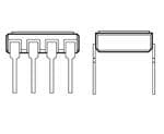
| 供应商器件封装 | 8-DIP |
| 其它名称 | 516-1943-5 |
| 包装 | 管件 |
| 安装类型 | 通孔 |
| 封装/外壳 | 8-DIP(0.300",7.62mm) |
| 工作温度 | -55°C ~ 125°C |
| 标准包装 | 1 |
| 电压-电源 | - |
| 电压-隔离 | 1500VDC |
| 类型 | 功率 MOSFET |
| 输入类型 | DC |


- 商务部:美国ITC正式对集成电路等产品启动337调查
- 曝三星4nm工艺存在良率问题 高通将骁龙8 Gen1或转产台积电
- 太阳诱电将投资9.5亿元在常州建新厂生产MLCC 预计2023年完工
- 英特尔发布欧洲新工厂建设计划 深化IDM 2.0 战略
- 台积电先进制程称霸业界 有大客户加持明年业绩稳了
- 达到5530亿美元!SIA预计今年全球半导体销售额将创下新高
- 英特尔拟将自动驾驶子公司Mobileye上市 估值或超500亿美元
- 三星加码芯片和SET,合并消费电子和移动部门,撤换高东真等 CEO
- 三星电子宣布重大人事变动 还合并消费电子和移动部门
- 海关总署:前11个月进口集成电路产品价值2.52万亿元 增长14.8%
PDF Datasheet 数据手册内容提取
HSSR-7110, HSSR-7111, HSSR-7112, 1 HSSR-711E, 5962-9314001, 5962-9314002 90V/1.0Ω, Hermetically Sealed, Power MOSFET Optocoupler Data Sheet Description Features The Broadcom® HSSR-7110, HSSR-7111, HSSR-7112, HSSR-711E Dual marked with device part number and DLA Standard and SMD 5962-9314001, 5962-9314002 are single-channel Microcircuit Drawing (SMD) power MOSFET optocouplers, constructed in eight-pin, ac/dc signal and power switching hermetic, dual-in-line, ceramic packages. The devices operate Compact solid-state bidirectional switch exactly like a solid-state relay. Manufactured and tested on a MIL-PRF-38534 certified line The products are capable of operation and storage over the full QML-38534, Class H and Class E military temperature range and can be purchased as a Hermetically sealed 8-pin, dual-in-line package commercial product (HSSR-7110), with full MIL-PRF-38534 Small size and weight Class H testing (HSSR-7111 and HSSR- 7112), with MIL-PRF-38534 Class E testing (Class K with exceptions) Performance guaranteed over –55°C to +125°C (HSSR-711E) or from the DLA Standard Microcircuit Drawing Connection A 0.8A, 1.0Ω (SMD) 5962-93140. Details of the Class E program exceptions Connection B 1.6A, 0.25Ω are listed here: 1500 Vdc withstand test voltage 1. Nondestructive Bond Pull, Test method 2023 of High transient immunity MIL-STD-883 in device screening is not required. 5 Amp output surge current 2. Particle Impact Noise Detection (PIND), Test method 2020 of MIL-STD-883 in device screening and group C testing is Applications not required. 3. Die Shear Strength, Test method 2019 of MIL-STD-883 in Military and space group B testing is not required. High reliability systems 4. Internal Water Vapor Content, Test method 1018 of Standard 28 Vdc and 48 Vdc load driver MIL-STD-883 in group C testing is not required. Standard 24 Vac load driver 5. Scanning Electron Microscope (SEM) inspections, Test Aircraft controls method 2018 of MIL-STD-883 in element evaluation is not ac/dc electromechanical and solid-state relay replacement required. I/O modules Harsh industrial environments CAUTION It is advised that normal static precautions be taken in handling and assembly of this 1. See Selection Guide – Lead Configuration Options for available component to prevent damage and/or extensions. degradation that may be induced by ESD. Broadcom - 1 -
HSSR-7110, HSSR-7111, HSSR-7112, HSSR-711E, 5962-9314001, 5962-9314002 Functional Diagrams Data Sheet Functional Diagrams The devices feature logic level input control and very low output on-resistance, making them suitable for both ac and dc CONNECTION A CONNECTION B loads. Connection A, as shown in the Functional Diagrams, AC/DC CONNECTION DC CONNECTION allows the device to switch either ac or dc loads. Connection B, IO IO 1 NC 8 + 1 NC 8 + with the polarity and pin configuration as shown, allows the IF IF VO device to switch dc loads only. The advantage of Connection B + 2 7 + 2 7 - is that the on-resistance is significantly reduced, and the VF VO VF - 3 6 - 3 6 output current capability increases by a factor of two. 4 NC 5 - 4 NC 5 The devices are convenient replacements for mechanical and solid-state relays where high component reliability with TRUTH TABLE standard footprint lead configuration is desirable. Devices may INPUT OUTPUT be purchased with a variety of lead bend and plating options. H CLOSED See Selection Guide – Lead Configuration Options table for L OPEN details. Standard microcircuit drawing (SMD) parts are available for each package and lead style. All devices are manufactured and tested on a MIL-PRF-38534 The HSSR-7110, HSSR-7111, HSSR-7112, HSSR-711E, and SMD certified line, and Class H and Class E devices are included in 5962-9314001, 5962-9314002 are designed to switch loads on the DLA Qualified Manufacturers List, QML-38534 for Hybrid 28 Vdc power systems. They meet 80V surge and ±600V spike Microcircuits. Each device contains an AlGaAs light-emitting requirements. diode optically coupled to a photovoltaic diode stack, which drives two discrete power MOSFETs. The device operates as a CAUTION Maximum Switching Frequency – Care should be solid-state replacement for single-pole, normally open (1 Form taken during repetitive switching of loads so as A) relay used for general-purpose switching of signals and not to exceed the maximum output current, loads in high reliability applications. maximum output power dissipation, maximum case temperature, and maximum junction temperature. Selection Guide – Lead Configuration Options Avago Technologies Part Number and Options Commercial HSSR-7110 MIL-PRF-38534 Class H HSSR-7111 HSSR-7112 MIL-PRF-38534 Class E HSSR-711E Standard Lead Finisha Gold Plate Gold Plate Gold Plate Solder Dippedb Option #200 Option -200 Option -200 Butt Joint/Gold Platea Option #100 Option -100 Gull Wing/Solderedb Option #300 Option -300 Option -300 Crew Cut/Gold Platea Option #600 Option -600 SMD Part Number Prescript for all below 5962- 5962- 5962- Gold Platea 9314001HPC 9314002HPC 9314001EPC Solder Dippedb 9314001HPA 9314002HPA 9314001EPA Butt Joint/Gold Platea 9314001HYC 9314002HYC Butt Joint/Solderedb 9314001HYA 9314002HYA Gull Wing/Solderedb 9314001HXA 9314002HXA 9314001EXA Crew Cut/Gold Platea 9314001HZC 9314002HZC Crew Cut/Solderedb 9314001HZA 9314002HZA a. Gold Plate lead finish: Maximum gold thickness of leads is <100 μin. Typical is 60 μin to 90 μin. b. Solder lead finish: Sn63/Pb37. Broadcom - 2 -
HSSR-7110, HSSR-7111, HSSR-7112, HSSR-711E, 5962-9314001, 5962-9314002 Outline Drawing Data Sheet Outline Drawing Device Marking AVAGO 8-Pin DIP Through Hole DESIGNATOR A QYYWWZ COMPLIANCE INDICATOR,[1] AVAGO P/N XXXXXX DATE CODE, SUFFIX DLA SMD[1] XXXXXXX (IF NEEDED) 10.03 (0.395) 8.13 (0.320) DLA SMD[1] XXX XXX COUNTRY OF MFR. 10.29 (0.405) MAX. PIN ONE/ 50434 AVAGO CAGE CODE[1] 1.02 (0.040) 7.16 (0.282) 1.52 (0.060) 7.57 (0.298) ESD IDENT [1] QML PARTS ONLY 4.32 (0.170) MAX. Thermal Resistance 0.51 (0.020) 3.81 (0.150) MIN. MIN. 0.20 (0.008) Maximum Output MOSFET Junction to Case – θJC = 15°C/W 0.33 (0.013) ESD Classification 7.36 (0.290) 2.29 (0.090) 0.51 (0.020) 7.87 (0.310) 2.79 (0.110) MAX. MIL-STD-883, Method 3015 , Class 2 NOTE: DIMENSIONS IN MILLIMETERS (INCHES). Hermetic Optocoupler Options Note: Dimensions in millimeters (inches). Option Description 100 Surface-mountable hermetic optocoupler with leads trimmed for butt joint assembly. This option is available on Commercial, Class H and E product. 4.32 (0.170) MAX. 0.51 (0.020) 1.14 (0.045) MIN. 1.40 (0.055) 0.20 (0.008) 0.33 (0.013) 2.29 (0.090) 0.51 (0.020) 2.79 (0.110) MAX. 7.36 (0.290) 7.87 (0.310) 200 Lead finish is solder dipped rather than gold plated. This option is available on Commercial, Class H and E product. DLA Drawing (SMD) part numbers contain provisions for lead finish. 300 Surface-mountable hermetic optocoupler with leads cut and bent for gull wing assembly. This option is available on Commercial, Class H and E product. This option has solder dipped leads. 4.57 (0.180) 4.57 (0.180) MAX. MAX. 0.20 (0.008) 0.51 (0.020) 1.40 (0.055) 5˚ MAX. 0.33 (0.013) MIN. 1.65 (0.065) 1.07 (0.042) 9.65 (0.380) 1.31 (0.052) 2.29 (0.090) 0.51 (0.020) 9.91 (0.390) 2.79 (0.110) MAX. 600 Surface-mountable hermetic optocoupler with leads trimmed for butt joint assembly. This option is available on Commercial, Class H and E product. 3.81 (0.150) MAX. 0.20 (0.008) 0.51 (0.020) 0.33 (0.013) MIN. 2.29 (0.090) 1.02 (0.040) 7.36 (0.290) 2.79 (0.110) TYP. 7.87 (0.310) Broadcom - 3 -
HSSR-7110, HSSR-7111, HSSR-7112, HSSR-711E, 5962-9314001, 5962-9314002 Absolute Maximum Ratings Data Sheet Absolute Maximum Ratings Parameter Symbol Min Max Unit Storage Temperature Range T –65 +150 °C S Operating Ambient Temperature T –55 +125 °C A Junction Temperature T — +150 °C J Operating Case Temperaturea TC — +145 °C Lead Solder Temperature — 260 for 10 s °C Average Input Current I — 20 mA F Peak Repetitive Input Current I — 40 mA FPK (Pulse Width < 100 ms; duty cycle < 50%) Peak Surge Input Current I — 100 mA FPK surge (Pulse Width < 0.2 ms; duty cycle < 0.1%) Reverse Input Voltage V — 5 V R Average Output Current (See Figure2.) I O Connection A — 0.8 A Connection B — 1.6 A Single Shot Output Current (See Figure3.) I OPK surge Connection A (Pulse width < 10 ms) — 5.0 A Connection B (Pulse width < 10 ms) — 10.0 A Output Voltage V O Connection A –90 90 V Connection B 0 90 V Average Output Power Dissipationb (See Figure4.) — 800 mW a. Maximum junction to case thermal resistance for the device is 15°C/W, where case temperature, T , is measured at the center of the package bottom. C b. For rating, see Figure4. The output power P rating curve is obtained when the part is handling the maximum average output current I as shown in Figure2. O O Recommended Operating Conditions Parameter Symbol Min Max Unit Input Current (on)a IF(ON) 5 20 mA Input Current (on)b IF(ON) 10 20 mA Input Voltage (off) V 0 0.6 V F(OFF) Operating Temperature T –55 +125 °C A a. Applies to HSSR-7112 and 5962-9314002Hxx devices only. b. Applies to HSSR-7110, HSSR-7111, HSSR-711E, 5962-9314001Hxx, and 5962-9314001Exx devices only. Broadcom - 4 -
HSSR-7110, HSSR-7111, HSSR-7112, HSSR-711E, 5962-9314001, 5962-9314002 Electrical Specifications Data Sheet Electrical Specifications T = –55°C to +125°C, unless otherwise specified. A Group A Parameter Symbol Test Conditions Min Typ Max Unit Figure Note Subgroupa Output Withstand Voltage |V | 1, 2, 3 V = 0.6V, I = 10 μA 90 110 — V 5 O(OFF) F O Output On-Resistance R 1, 2, 3 I = 10 mA, I = 800 mA, — 0.40 1.0 Ω 6, 7 b, c (ON) F O Connection A (pulse duration ≤ 30 ms) I = 5 mA, I = 800 mA, — — 1.0 b, d F O (pulse duration ≤ 30 ms) Output On-Resistance R 1, 2, 3 I = 10 mA, I = 1.6A, — 0.12 0.25 Ω 6, 7 b, c (ON) F O Connection B (pulse duration ≤ 30 ms) I = 5 mA, I = 1.6A, — — 0.25 b, d F O (pulse duration ≤ 30 ms) Output Leakage Current IO(OFF) 1, 2, 3 VF = 0.6V, VO = 90V — 10-4 10 μA 8 Input Forward Voltage V 1, 2, 3 I = 10 mA 1.0 1.24 1.7 V 9 c F F I = 5 mA — — — d F Input Reverse Breakdown V 1, 2, 3 I = 100 μA 5.0 — — V R R Voltage Input-Output Insulation II-O 1 RH ≤ 65%, t = 5s, — — 1.0 μA e, f V = 1500 Vdc, T = 25°C I-O A Turn On Time t 9, 10, 11 I = 10 mA, V = 28V, — 1.25 6.0 ms 1, 10, c ON F DD I = 800 mA 11, 12, O 13 I = 5 mA, V = 28V, I = 800 mA — — 6.0 d F DD O Turn Off Time t 9, 10, 11 I = 10 mA, V = 28V, — 0.02 0.25 ms 1, 10, c OFF F DD I = 800 mA 14, 15 O I = 5 mA, V = 28V, I = 800 mA — — 0.25 d F DD O Output Transient Rejection 9 V = 50V, C = 1000 pF, 1000 — — V/μs 17 dVo PEAK M ---------- dt CL = 15 pF, RM ≥ 1 MΩ Input-Output Transient 9 V = 5V, V = 50V, 500 — — V/μs 18 dVio DD I-O(PEAK) Rejection ----------- dt RL = 20 kΩ, CL = 15 pF a. Commercial parts receive 100% testing at 25°C (Subgroups 1 and 9). SMD, Class H, and Class E parts receive 100% testing at 25°C, 125°C, and –55°C (subgroups 1 and 9, 2 and 10, 3 and 11, respectively). b. During the pulsed R measurement (I duration <30 ms), ambient (T ) and case temperature (T ) are equal. ON O A C c. Applies to HSSR-7110, HSSR-7111, HSSR-711E, 5962-9314001Hxx and 5962-9314001Exx devices only. d. Applies to HSSR-7112 and 5962-9314002Hxx devices only. e. Device considered a two-terminal device: pins 1 through 4 shorted together and pins 5 through 8 shorted together. f. This is a momentary withstand test, not an operating condition. Broadcom - 5 -
HSSR-7110, HSSR-7111, HSSR-7112, HSSR-711E, 5962-9314001, 5962-9314002 Typical Characteristics Data Sheet Typical Characteristics All typical values are at T = 25°C, I (ON) = 10 mA, V (OFF) = 0.6V unless otherwise specified. A F F Parameter Symbol Test Conditions Typ Unit Figure Output Off-Capacitance C V = 28V, f = 1 MHz 145 pF 16 O(OFF) O Output Offset Voltagea |VOS| IF = 10 mA, IO = 0 mA 2 μV 19 Input Diode Temperature Coefficient ΔV /ΔT I = 10 mA –1.4 mV/°C F A F Input Capacitanceb CIN VF = 0V, f = 1 MHz 20 pF Input-Output Capacitancec CI-O VI-O = 0V, f = 1 MHz 1.5 pF Input-Output Resistancec RI-O VI-O = 500V, t = 60s 1013 Ω Turn On Time With Peakingd tON IFPK = 100 mA, IFSS = 10 mA, 0.22 ms 1 V = 28V, I = 800 mA DD O a. V is a function of I , and is defined between pins 5 and 8, with pin 5 as the reference. V must be measured in a stable ambient (free of temperature OS F OS gradients). b. Zero-bias capacitance measured between the LED anode and cathode. c. Device considered a two-terminal device: pins 1 through 4 shorted together and pins 5 through 8 shorted together. d. For a faster turn-on time, the optional peaking circuit shown in Figure1 can be implemented. Figure1 Recommended Input Circuit HSSR-711x 1 8 VCC (+5V) IF + 2 7 VF - 3 6 R2 1200 (cid:58) R3 4 5 R1 330 (cid:58) C 15 μF IN 1/4 54ACTOO R1 = REQUIRED CURRENT LIMITING RESISTOR FOR IF (ON)= 10 mA. 1/4 54ACTOO* R2 = PULL-UP RESISTOR FOR VF (OFF) < 600 mV; IF (VCC- VOH ) < 600 mV, OMIT R2. R3, C = OPTIONAL PEAKING CIRCUIT. TYPICAL VALUES R3 IF (PK) HSSR-711x ((cid:58)) (mA) tON (ms) - 10 (NO PK) 2.0 * USE SECOND GATE IF IF (PK) > 50 mA 330 20 1.0 REMINDER: TIE ALL UNUSED INPUTS TO GROUND OR VCC 100 40 0.48 33 100 0.22 Broadcom - 6 -
HSSR-7110, HSSR-7111, HSSR-7112, HSSR-711E, 5962-9314001, 5962-9314002 Typical Characteristics Data Sheet Figure2 Maximum Average Output Current Rating vs. Ambient Figure3 Single Shot (Non-Repetitive) Output Current vs. Pulse Temperature Duration 1.0 12 IF 10 mA 11 0.8 A T - 10 N UT CURRENT - A 00..46 UTPUT CURRE 798 CONNECTION-B I - OUTPO 0.2 CIFO N N 1E0C TmCCIAAOA N =-= A 8400˚˚CC//WW SURGE - OK 645 CONNECTION-A 0-55 -25 5 35 65 95 125 155 IOP 3 10 200 400 600 800 1000 TA - AMBIENT TEMPERATURE - ˚C PULSE DURATION - ms Figure4 Output Power Rating vs. Ambient Temperature Figure5 Normalized Typical Output Withstand Voltage vs. Temperature 1.0 1.10 VF = 0.6 V 0.8 1.08 IO = 10 μA 1.06 W P - OUTPUT POWER DISSIPATION - O 000...6240 CIFO N N 1E0C TmCCIAAOA N =-= A 8400˚˚CC//WW NORMALIZED TYPICAL OUTPUTWITHSTAND VOLTAGE 000111......999000468024 -55 -25 5 35 65 95 125 155 0.92 -55 -25 5 35 65 95 125 TA - AMBIENT TEMPERATURE - ˚C TA - AMBIENT TEMPERATURE - ˚C Figure6 Normalized Typical Output Resistance vs. Temperature Figure7 Typical On State Output I-V Characteristics 1.8 0.8 CONNECTION - A CONNECTION - A IF 10 mA 0.6 IO 10 mA 1.6 (IPOU =LS 8E0 D0U mRAATION 30 ms) 0.4 I O ( P3U0 LmSEs) DURATION 1.4 0.2 A NORMALIZED TYPICAL OUTPUT RESISTANCE 011...802 - OUTPUT CURRENT - IO ---000...6420 TTTAAA === 21-5525˚5˚C˚CC 0.6 -0.8 -55 -25 5 35 65 95 125 -0.6 -0.4 -0.2 0 0.2 0.4 0.6 TA - AMBIENT TEMPERATURE - ˚C VO - OUTPUT VOLTAGE - V Broadcom - 7 -
HSSR-7110, HSSR-7111, HSSR-7112, HSSR-711E, 5962-9314001, 5962-9314002 Typical Characteristics Data Sheet Figure8 Typical Output Leakage Current vs. Temperature Figure9 Typical Input Forward Current vs. Input Forward Voltage 10-7 10-1 CONNECTION A 10-8 VVFO == 09.06 VV 10-2 A RENT - NT - A 10-3 UTPUT LEAKAGE CUR 1100-1-09 UT FORWARD CURRE 1100--45 TA = 125˚C TA = 25˚C - OIO (OFF)10-1120 35 65 95 125 - INPIF 10-60.4 0.6 0.8 1.0 1.2TA =1. -455˚C 1.6 TA - TEMPERATURE - ˚C VF - INPUT FORWARD VOLTAGE - V Figure10 Switching Test Circuit for t , t ON OFF VDD PULSE GEN. 50% 50% IF tfZ =O t =r =50 5 ns HSSR-711x RL P.W. = 15 ms 1 8 VO IF MONITOR NODE + 2 7 VF CL = 25 pF - 3 6 (CL INCLUDES PROBE AND FIXTURE CAPACITANCE) VO 90% 4 5 10% MONITIFOR R (MONITOR) 200 tON tOFF GND GND Broadcom - 8 -
HSSR-7110, HSSR-7111, HSSR-7112, HSSR-711E, 5962-9314001, 5962-9314002 Typical Characteristics Data Sheet Figure11 Typical Turn On Time vs. Temperature Figure12 Typical Turn On Time vs. Input Current 2.6 3.0 CONNECTION A CONNECTION A 2.4 IF = 10 mA 2.6 VDD = 28 V 2.2 IVOD D= 8=0 208 m VA 2.2 TIOA = = 8 2050˚ CmA 2.0 ME - ms 1.8 ME - ms 1.8 - TURN ON TI 111...642 - TURN ON TI 11..40 TON 1.0 TON 0.6 0.8 0.2 -55 -25 5 35 65 95 125 5 10 15 20 TA - TEMPERATURE - ˚C IF - INPUT CURRENT - mA Figure13 Typical Turn On Time vs. Voltage Figure14 Typical Turn Off Time vs. Temperature 2.0 15.0 CONNECTION - A 111...486 TIIFOA === 8120050 ˚m CmAA 1144..68 ICIVFOOD ND ==N 1=8E0C0 2 T0m8I OmA VNA A 14.4 ME - ms 11..02 ME - μs 14.2 - TURN ON TIN 000...864 - TURN OFF TI 111433...086 TO 0.2 TOFF 13.4 0 13.2 0 10 20 30 40 50 60 70 80 90 -55 -25 5 35 65 95 125 VDD - VOLTAGE - V TA-TEMPERATURE - ˚C Figure15 Typical Turn Off Time vs. Input Current Figure16 Typical Output Off Capacitance vs. Output Voltage 45 440 CONNECTION A CONNECTION A 40 VDD = 28 V 400 f = 1 MHz 35 ITOA = = 8 2050˚ CmA NCE - pF 360 TA = 25˚C T - TURN OFF TIME - μsOFF 3221105050 - OUTPUT OFF CAPACITAO(OFF)322212840600000 5 C 120 5 10 15 20 0 5 10 15 20 25 30 IF - INPUT CURRENT - mA VO(OFF) - OUTPUT VOLTAGE - V Broadcom - 9 -
HSSR-7110, HSSR-7111, HSSR-7112, HSSR-711E, 5962-9314001, 5962-9314002 Typical Characteristics Data Sheet Figure17 Output Transient Rejection Test Circuit HSSR-711x VM 1 8 MONITOR IF NODE INPUT OPEN + 2 7 CM RM VF - 3 6 VPEAK + - 4 5 PULSE GENERATOR CM INCLUDES PROBE AND FIXTURE CAPACITANCE RM INCLUDES PROBE AND FIXTURE RESISTANCE 90% 90% VPEAK 10% 10% tr tf VM (MAX) 5 V ddVtO =(0.8) Vtr(PEAK) OR (0.8) Vtf(PEAK) OVERSHOOT ON VPEAK IS TO BE 10%. Figure18 Input-Output Transient Rejection Test Circuit VDD HSSR-711x RL 1 8 VO IF + 2 7 CL V-F 3 6 F(CIXLT UINRCEL CUADPEASC PITRAONBCEE P )LUS S1 A 4 5 B VIN VI-O + - PULSE GENERATOR 90% 90% VI-O(PEAK) 10% 10% tr tf VO(OFF) S1 AT A (VF = 0 V) VO(OFF) (min) 3.25 V VO(ON) (max) 0.8 VO(ON) S1 AT B (IF = 10 mA)11 OR (I F = 5 mA)10 dVdIt-O = (0.8) VIt-rO(PEAK) OR (0.8) VI-tOf(PEAK) OVERSHOOT ON VI-O(PEAK) IS TO BE 10% Broadcom - 10 -
HSSR-7110, HSSR-7111, HSSR-7112, HSSR-711E, 5962-9314001, 5962-9314002 Applications Information Data Sheet Figure19 Voltage Offset Test Setup Figure21 Thermal Model ISOTHERMAL CHAMBER Tje Tjf1 Tjd Tjf2 HSSR-711x IF 1 8 + 104 15 15 15 TC +2 7 VOS NANODVOIGLITTMALE TER - 3 6 CA 4 5 - TA T je = LED JUNCTION TEMPERATURE Tjf1 = FET 1 JUNCTION TEMPERATURE Figure20 Burn-In Circuit Tjf2 = FET 2 JUNCTION TEMPERATURE Tjd = FET DRIVER JUNCTION TEMPERATURE 1 HSSR-711x 8 ROUT (VSOEE NOTE) TC = COAFS PEA TCEKMAPGEER BAOTTUTROEM ()MEASURED AT CENTER 1.0 TA = AMBIENT TEMPERATURE (MEASURED 6" AWAY 2 7 FROM THE PACKAGE) VIN RIN 3 6 CA = CASE-TO-AMBIENT THERMAL RESISTANCE 5.5 V 200 4 5 ROUT ALL THERMAL RESISTANCE VALUES ARE IN ˚C/W 1.0 On-Resistance and Rating Curves NOTE: IN ORDER TO DETERMINE VOUT CORRECTLY, THE CASE TO AMBIENT THERMAL IMPEDANCE MUST BCOER MREEACSTU ORUETDP FUOTR C TUHRER EBNUTR PNE-IRN F BIGOUARREDSS 2T OA NBDE U4 STEOD I.N TSHUERNE, TKHNAOTW TIHNEG D EVCAIC, ED METEEERTMS ITNHEE THE The output on-resistance, RON, specified in this data sheet, is DERATING REQUIREMENTS AS SHOWN. the resistance measured across the output contact when a pulsed current signal (I = 800 mA) is applied to the output O pins. The use of a pulsed signal (≤30 ms) implies that each Applications Information junction temperature is equal to the ambient and case temperatures. The steady-state resistance, R , on the other SS Thermal Model hand, is the value of the resistance measured across the output contact when a DC current signal is applied to the output pins The steady-state thermal model for the HSSR-711x is shown in for a duration sufficient to reach thermal equilibrium. R SS Figure21. The thermal resistance values given in this model includes the effects of the temperature rise of each element in can be used to calculate the temperatures at each node for a the thermal model. Rating curves are shown in Figure2 and given operating condition. The thermal resistances between Figure4. Figure2 specifies the maximum average output the LED and other internal nodes are very large in comparison current allowable for a given ambient temperature. Figure4 with the other terms and are omitted for simplicity. The specifies the output power dissipation allowable for a given components do, however, interact indirectly through θ , the CA ambient temperature. Above 55°C (for θ = 80°C/W) and CA case-to-ambient thermal resistance. All heat generated flows 107°C (for θ =40°C/W/W), the maximum allowable output CA through θ , which raises the case temperature T accordingly. CA C current and power dissipation are related by the expression The value of θCA depends on the conditions of the board R = P / (I )2 from which R can be calculated. SS O(max) O(max) SS design and is, therefore, determined by the designer. Staying within the safe area assures that the steady-state The maximum value for each output MOSFET junction-to-case junction temperatures remain less than 150°C. As an example, thermal resistance is specified as 15°C/W. The thermal for TA=95°C and θCA=80°C/W, Figure2 shows that the output resistance from FET driver junction-to-case is also 15°C/W/W. current should be limited to less than 610mA. A check with The power dissipation in the FET driver, however, is negligible Figure4 shows that the output power dissipation at TA = 95°C in comparison to the MOSFETs. and IO=610mA, is limited to less than 0.35W. This yields an RSS of 0.94Ω. Broadcom - 11 -
HSSR-7110, HSSR-7111, HSSR-7112, HSSR-711E, 5962-9314001, 5962-9314002 Design Considerations for Replacement of Electromechanical Relays Data Sheet Design Considerations for Replacement of Output Circuit Electromechanical Relays Unlike with electromechanical relays, when considering The HSSR-711x family can replace electromechanical relays solid-state relays, the designer should pay careful attention to with comparable output voltage and current ratings. The the output on-resistance. The previous section, On-Resistance following design issues need to be considered in the and Rating Curves, describes the issues that need to be replacement circuit. considered. In addition, for strictly dc applications, the designer has an advantage using Connection B, which has twice the output current rating as Connection A. Furthermore, Input Circuit for dc-only applications, with Connection B the on-resistance is considerably less when compared to Connection A. The drive circuit of the electromechanical relay coil needs to be modified so that the average forward current driving the LED Output over-voltage protection is yet another important of the HSSR-711x does not exceed 20 mA. A nominal forward design consideration when replacing electromechanical relays drive current of 10 mA is recommended. A recommended drive with the HSSR-711x. The output power MOSFETs can be circuit with 5V VCC and CMOS logic gates is shown in Figure1. protected using Metal oxide varistors (MOVs) or TransZorbs If higher VCC voltages are used, adjust the current limiting against voltage surges that exceed the 90V output withstand resistor to a nominal LED forward current of 10 mA. One voltage rating. Examples of sources of voltage surges are important consideration to note is that when the LED is turned inductive load kickbacks, lightning strikes, and electrostatic off, no more than 0.6V forward bias should be applied across voltages that exceed the specifications on this data sheet. For the LED. Even a few microamps of current may be sufficient to more information on output load and protection, refer to turn on the HSSR- 711x, although it may take a considerable Application Note 1047. time. The drive circuit should maintain at least 5 mA of LED current during the ON condition. If the LED forward current is References less than the 5 mA level, it causes the HSSR-711x to turn on with a longer delay. In addition, the power dissipation in the Application Note 1047, Low On-Resistance Solid State Relays output power MOSFETs increases, which, in turn, may violate for High Reliability Applications. the power dissipation guidelines and affect the reliability of the Reliability Data for HSSR-7111, HSSR-7112, and HSSR-711E. device. Broadcom - 12 -
For product information and a complete list of distributors, please go to our web site: www.broadcom.com. Broadcom, the pulse logo, Connecting everything, Avago Technologies, Avago, and the A logo are among the trademarks of Broadcom in the United States, certain other countries and/or the EU. Copyright © 2016–2017 Broadcom. All Rights Reserved. The term "Broadcom" refers to Broadcom Limited and/or its subsidiaries. For more information, please visit www.broadcom.com. Broadcom reserves the right to make changes without further notice to any products or data herein to improve reliability, function, or design. Information furnished by Broadcom is believed to be accurate and reliable. However, Broadcom does not assume any liability arising out of the application or use of this information, nor the application or use of any product or circuit described herein, neither does it convey any license under its patent rights nor the rights of others. AV02-3835EN – October 19, 2017
Mouser Electronics Authorized Distributor Click to View Pricing, Inventory, Delivery & Lifecycle Information: B roadcom Limited: 5962-9314001HPA 5962-9314001HPC 5962-9314001HXA 5962-9314001HYA 5962-9314001HYC 5962- 9314001HZA 5962-9314001HZC 5962-9314002HPA 5962-9314002HPC 5962-9314002HXA 5962-9314002HYA HSSR-7110 HSSR-7110#100 HSSR-7110#200 HSSR-7110#300 HSSR-7110#600 HSSR-7111 HSSR-7111#100 HSSR-7111#200 HSSR-7111#300 HSSR-7111#600 HSSR-7112-200 5962-9314002HYC 5962-9314002HZC 5962- 9314002HZA 5962-9314001EPC HSSR-7112-100 HSSR-7112-600 HSSR-7112 5962-9314001EPA HSSR-7112- 300 HSSR-711E-200 HSSR-711E HSSR-711E-300 5962-9314001EXA