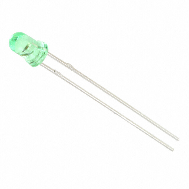
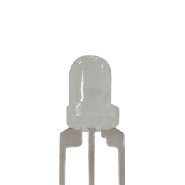
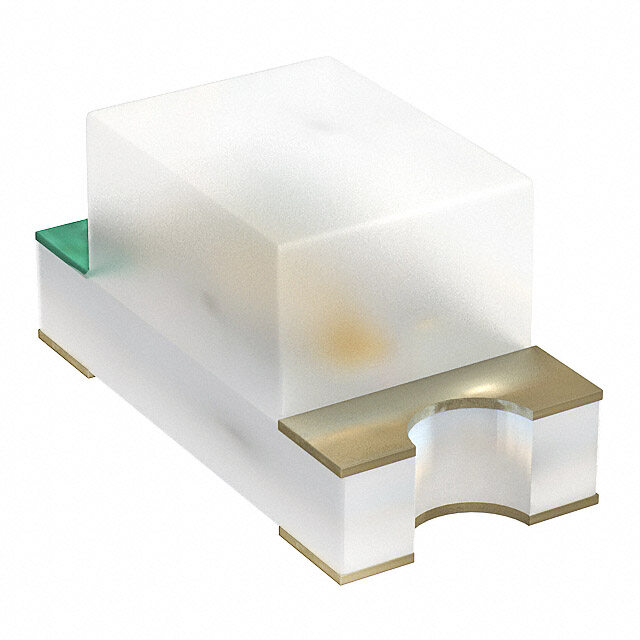
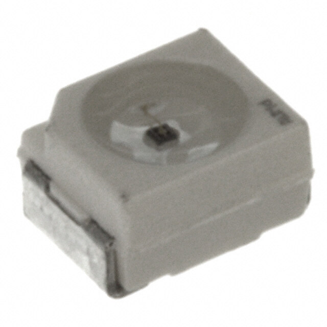
ICGOO在线商城 > 光电元件 > LED 指示 - 分立 > HSMF-C165
- 型号: HSMF-C165
- 制造商: Avago Technologies
- 库位|库存: xxxx|xxxx
- 要求:
| 数量阶梯 | 香港交货 | 国内含税 |
| +xxxx | $xxxx | ¥xxxx |
查看当月历史价格
查看今年历史价格
HSMF-C165产品简介:
ICGOO电子元器件商城为您提供HSMF-C165由Avago Technologies设计生产,在icgoo商城现货销售,并且可以通过原厂、代理商等渠道进行代购。 HSMF-C165价格参考¥1.05-¥1.05。Avago TechnologiesHSMF-C165封装/规格:LED 指示 - 分立, Green, Red 572nm Green, 621nm Red LED Indication - Discrete 2.2V Green, 1.95V Red 0603 (1608 Metric)。您可以下载HSMF-C165参考资料、Datasheet数据手册功能说明书,资料中有HSMF-C165 详细功能的应用电路图电压和使用方法及教程。
| 参数 | 数值 |
| 产品目录 | |
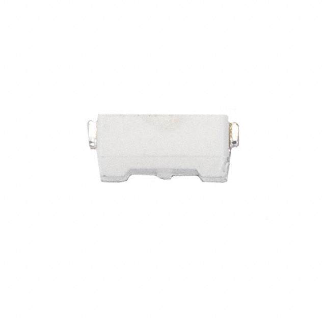
| 描述 | LED BICOLOR HER/GN DIFF 0603 SMD标准LED-SMD Grn/Red Bi-Color |
| 产品分类 | |
| LED大小 | 1.6 mm x 0.8 mm x 0.5 mm |
| 品牌 | Avago Technologies |
| 产品手册 | |
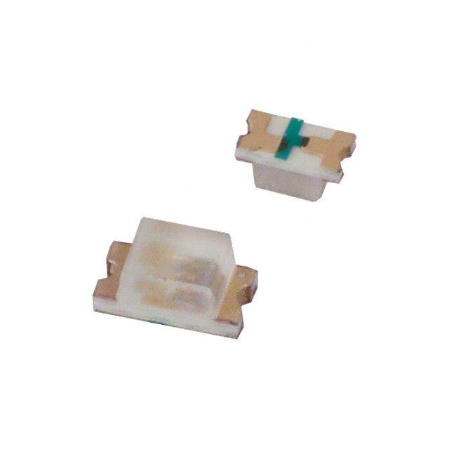
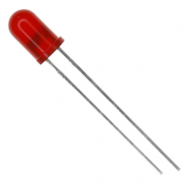
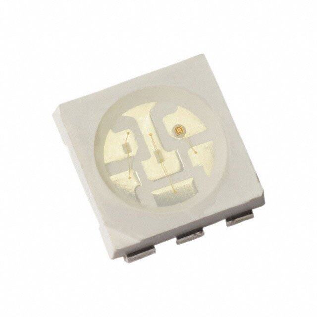
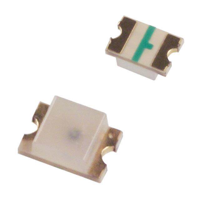
| 产品图片 |
|
| rohs | 符合RoHS无铅 / 符合限制有害物质指令(RoHS)规范要求 |
| 产品系列 | LED发射器,标准LED-SMD,Avago Technologies HSMF-C165- |
| 数据手册 | http://www.avagotech.com/docs/AV02-0584EN |
| 产品型号 | HSMF-C165 |
| 产品目录绘图 |
|
| 产品目录页面 | |
| 产品种类 | 标准LED-SMD |
| 光强度 | 15 mcd, 10 mcd |
| 其它名称 | 516-1419-6 |
| 包装 | Digi-Reel® |
| 商标 | Avago Technologies |
| 大小/尺寸 | 1.60mm 长 x 0.80mm 宽 |
| 安装类型 | 表面贴装 |
| 封装 | Reel |
| 封装/外壳 | 0603(1608 公制) |
| 封装/箱体 | 0603 |
| 工厂包装数量 | 4000 |
| 显示角 | 120 deg |
| 最大工作温度 | + 85 C |
| 最小工作温度 | - 40 C |
| 标准包装 | 1 |
| 正向电压 | 2.1 V, 2.2 V |
| 正向电流 | 20 mA |
| 毫烛光等级 | 15mcd 绿,10mcd 红 |
| 波长-主 | 572nm,621nm |
| 波长-峰值 | 570nm,636nm |
| 波长/色温 | 626 nm, 572 nm |
| 测试电流时的光通量 | - |
| 照明颜色 | Red, Green |
| 电压-正向(Vf)(典型值) | 2.2V 绿,2.1V 红 |
| 电流-测试 | 20mA |
| 视角 | 120° |
| 透镜样式/尺寸 | 矩形,带平顶,1.6mm x 0.8mm |
| 透镜类型 | 散射 |
| 透镜颜色/类型 | Untinted Diffused |
| 颜色 | 绿,红 |
| 高度 | 0.50mm |


- 商务部:美国ITC正式对集成电路等产品启动337调查
- 曝三星4nm工艺存在良率问题 高通将骁龙8 Gen1或转产台积电
- 太阳诱电将投资9.5亿元在常州建新厂生产MLCC 预计2023年完工
- 英特尔发布欧洲新工厂建设计划 深化IDM 2.0 战略
- 台积电先进制程称霸业界 有大客户加持明年业绩稳了
- 达到5530亿美元!SIA预计今年全球半导体销售额将创下新高
- 英特尔拟将自动驾驶子公司Mobileye上市 估值或超500亿美元
- 三星加码芯片和SET,合并消费电子和移动部门,撤换高东真等 CEO
- 三星电子宣布重大人事变动 还合并消费电子和移动部门
- 海关总署:前11个月进口集成电路产品价值2.52万亿元 增长14.8%

PDF Datasheet 数据手册内容提取
HSMF-C16x Miniature Bi-Color Surface Mount ChipLEDs Data Sheet Description Features This series of bi-color ChipLEDs is designed with the small- • Small size est footprint to achieve high density of components on • 0603 industry standard footprint board. They have the industry standard footprint of 1.6 • Diffused optics mm x 0.8 mm and a height of only 0.5 mm. This makes them very suitable for cellular phone and mobile equip- • Operating temperature range of –40° C to +85° C ment backlighting and indication. They are available in • Compatible with reflow soldering a wide range of color combinations. In order to facilitate • Available in various color combination automated pick and place operation, these ChipLEDs are shipped in tape and reel, with 4000 units per reel. These • Available in 8 mm tape on 7" (178 mm) diameter parts are compatible with reflow soldering. reels Applications • Keypad backlighting • Symbol indicator • LCD backlighting • Pushbutton backlighting • Front panel indicator Device Selection Guide Part Number Color Package Description HSMF-C162 AlInGaP Red / AlInGaP Amber Untinted, Diffused HSMF-C163 AlInGaP Red / InGaN Green Untinted, Diffused HSMF-C164 AlInGaP Red / InGaN Blue Untinted, Diffused HSMF-C165 High Efficiency Red / GaP Green Untinted, Diffused HSMF-C166 GaP Yellow / GaP Green Untinted, Diffused HSMF-C167 GaP Orange / GaP Green Untinted, Diffused HSMF-C168 InGaN Green / InGaN Blue Untinted, Diffused HSMF-C169 AlInGaP Amber / InGaN Blue Untinted, Diffused CAUTION: HSMF-C16x LEDs are class 1A ESD sensitive per JESD22-A114C.01 standard. Please observe appropriate pre- cautions during handling and processing. Refer to Avago Technologies Application Note AN-1142 for additional details.
Package Dimensions LED DIES CATHODE LINE 1 3 0.8 (0.031) 2 4 1.6 (0.063†) DIFFUSED EPOXY 0.5 (0.020) PC BOARD 0.16 (0.006) CATHODE LINE 0.4 (0.016) 0.3 (0.012) SOLDERING TERMINALS POLARITY HSMF-C162 HSMF-C163 HSMF-C164 HSMF-C165 HSMF-C166 HSMF-C167 HSMF-C168 HSMF-C169 1 3 AMBER GREEN BLUE GREEN GREEN GREEN BLUE BLUE 2 4 RED RED RED RED YELLOW ORANGE GREEN AMBER NoTES: 1. All DIMENSIoNS IN MIllIMETERS (INCHES). 2. TolERANCE IS ± 0.1 MM (± 0.004 IN.) UNlESS oTHERwISE SPECIFIED. Absolute Maximum Ratings for Each Die at TA = 25° C Parameter AlInGaP InGaN GaP Units DC Forward Current [1] 20 10 20 mA Power Dissipation 48 38 52 mW Reverse Voltage 5 5 5 V LED Junction Temperature 95 95 95 ˚C Operating Temperature Range –40 to +85 ˚C Storage Temperature Range –40 to +85 ˚C Soldering Temperature See reflow soldering profile (Figure 6 & 7) Note: 1. Derate linearly as shown in Figure 4. 2
Electrical Characteristics at TA = 25° C Reverse Breakdown Capacitance Thermal Forward Voltage VR (Volts) C (pF), @ VF = 0, Resistance VF (Volts) @ IF[1] @ IR = 100 µA f = 1 MHz RθJ-PIN (°C/w) Color Typ. Max. Min. Typ. Typ. AlInGaP Red 20 mA 1.9 2.4 5 15 300 AlInGaP Amber 20 mA 1.9 2.4 5 11 300 AlInGaP Red[2] 10 mA 1.8 2.3 5 15 300 AlInGaP Amber[2] 10 mA 1.8 2.3 5 11 300 InGaN Green 10 mA 3.4 3.8 5 35 500 InGaN Blue 10 mA 3.4 3.8 5 35 500 HER 20 mA 1.95 2.6 5 5 325 GaP Orange 20 mA 2.2 2.6 5 7 325 GaP Yellow 20 mA 2.1 2.6 5 6 325 GaP Green 20 mA 2.2 2.6 5 9 325 Notes: 1. VF Tolerance: ± 0.1 V. 2. The product testing is based on 20 mA. This is for reference only. optical Characteristics at TA = 25° C Color Peak Dominant luminous luminous Intensity wavelength wavelength Viewing Angle Efficacy Iv (mcd) @ IF[1] λpeak (nm) λd[2] (nm) 2 θ1/2 Degrees[3] ηv (lm/w) Color Min. Typ. Typ. Typ. Typ. Typ. AlInGaP Red 20 mA 28.5 90 637 626 120 155 AlInGaP Amber 20 mA 28.5 90 595 592 120 480 AlInGaP Red[4] 10 mA 11.2 35 637 626 120 155 AlInGaP Amber[4] 10 mA 11.2 35 595 592 120 480 InGaN Green 10 mA 18 45 523 525 120 500 InGaN Blue 10 mA 2.8 10 468 470 120 80 HER 20 mA 2.8 10 636 621 120 145 GaP Orange 20 mA 2.8 8 605 604 120 380 GaP Yellow 20 mA 2.8 8 589 586 120 500 GaP Green 20 mA 4.5 15 570 572 120 595 Notes: 1. The luminous intensity Iv is measured at the peak of the spatial radiation pattern which may not be aligned with the mechanical axis of the lamp package. 2. The dominant wavelength λd is derived from the CIE Chromatically Diagram and represents the perceived color of the device. 3. θ1/2 is the off-axis angle where the luminous intensity is 1/2 the peak intensity. 4. The product testing is based on 20 mA. This is for reference purpose. 3
Color Bin limits[1] Intensity (Iv) Bin limits[1] Intensity @ 20 mA (mcd) Green Color Bins[1] Yellow/Amber Color Bins[1] Bin ID Min. Max. Dom. wavelength (nm) Dom. wavelength (nm) A 0.11 0.18 Bin ID Min. Max. Bin ID Min. Max. B 0.18 0.29 A 561.5 564.5 A 582.0 584.5 C 0.29 0.45 B 564.5 567.5 B 584.5 587.0 D 0.45 0.72 C 567.5 570.5 C 587.0 589.5 E 0.72 1.10 D 570.5 573.5 D 589.5 592.0 F 1.10 1.80 E 573.5 576.5 E 592.0 594.5 G 1.80 2.80 Tolerance: ± 0.5 nm F 594.5 597.0 H 2.80 4.50 Tolerance: ± 0.5 nm J 4.50 7.20 Blue Color Bins[1] K 7.20 11.20 Dom. wavelength (nm) InGaN Green Color Bins[1] L 11.20 18.00 Bin ID Min. Max. Dom. wavelength (nm) M 18.00 28.50 A 460.0 465.0 Bin ID Min. Max. N 28.50 45.00 B 465.0 470.0 A 515.0 520.0 P 45.00 71.50 C 470.0 475.0 B 520.0 525.0 Q 71.50 112.50 D 475.0 480.0 C 525.0 530.0 R 112.50 180.00 Tolerance: ± 1 nm D 530.0 535.0 S 180.00 285.00 Tolerance: ± 1 nm T 285.00 450.00 orange Color Bins[1] U 450.00 715.00 Dom. wavelength (nm) V 715.00 1125.00 Bin ID Min. Max. W 1125.00 1800.00 A 597.0 600.0 X 1800.00 2850.00 B 600.0 603.0 Y 2850.00 4500.00 C 603.0 606.0 Tolerance: ± 15%. D 606.0 609.0 E 609.0 612.0 F 612.0 615.0 Note: 1. Bin categories are established for classifi- Tolerance: ± 1 nm cation of products. Products may not be available in all categories. Please contact your Avago representative for information Note: on currently available bins. 1. Bin categories are established for classifi- cation of products. Products may not be available in all categories. Please contact your Avago representative for information on currently available bins. 4
100 1.0 90 InBGLaUNE AMBEARS AOSRANGE GaP GREEN InGaN 80 GREEN AS RELATIVE INTENSITY – %5376400000 RED RELATIVE INTENSITY0.5 GGaaPP OYERLALNOGWE HER 20 10 0 0 400 450 500 550 600 650 700 500 550 600 650 700 750 WAVELENGTH – nm WAVELENGTH - nm Figure 1. Relative intensity vs. wavelength. HSMF-C16x fig 1 100 100 AS AlInGaP I – FORWARD CURRENT – mAF 101 InGaN I – FORWARD CURRENT – mAF 101 ORANHGaGERPE GGaaPP YGERLELEONW 0.1 0 1.5 2.0 2.5 3.0 3.5 4.0 1.5 1.6 1.7 1.8 1.9 2 2.1 2.2 2.3 VF – FORWARD VOLTAGE – V VF – FORWARD VOLTAGE – V Figure 2. Forward current vs. forward voltage. HSMF-C16x fig 2 1.4 1.6 1.4 1.2 1.4 1.2 1.2 LUMINOUS INTENSITY(NORMALIZED AT 20 mA) 0100....8064 AS AlInGaP LUMINOUS INTENSITY(NORMALIZED AT 10 mA) 0010....6804 InGaN LUMINOUS INTENSITY(NORMALIZED AT 20 mA) 0001....6840 GaP 0.2 0.2 0.2 0 0 0 0 5 10 15 20 25 30 0 2 4 6 8 10 12 14 16 0 5 10 15 20 25 30 IF – FORWARD CURRENT – mA IF – FORWARD CURRENT – mA IF – FORWARD CURRENT – mA Figure 3. luminous intensity vs. forward current. HSMF-C16x fig 3a HSMF-C16x fig 3b 5
25 100 mA 90 – AlInGaP/GaP NT 20 80 URRE – %70 M FORWARD C 1150 InGaN VE INTENSITY 654000 AXIMU RELATI30 – M 5 20 MAX. 10 IF 0 0 0 10 20 30 40 50 60 70 80 90 100 -90 -80 -70 -60 -50 -40 -30 -20 -10 0 10 20 30 40 50 60 70 80 90 TA – AMBIENT TEMPERATURE – °C ANGLE Figure 4. Maximum forward current vs. ambient Figure 5. Relative intensity vs. angle. temperature. HSMF-C16x fig 5 10 - 30 SEC. 255 - 260°C 10 SEC. MAX. 3°C/SEC. MAX. RE 217°C PERATURE 140-160°C 230°C MAX. 4°C/SEC. MAX. TEMPERATU 210500°°CC 3°C/SEC. MAX. 6°C/SEC. MAX. TEM 4°CM/SAEXC.. 3°C/SEC. MAX. 60 - 120 SEC. 100 SEC. MAX. OVER 2 MIN. TIME TIME (Acc. to J-STD-020C) Figure 6. Recommended reflow soldering profile. Figure 7. Recommended Pb-free reflow soldering profile. 0.60 (0.024) 0.40 0.30 (0.016) (0.012) 0.40 (0.016) 0.70 0.70 (0.028) (0.028) Figure 8. Recommended soldering pad pattern. HSMF-C16x fig 7 6
USER FEED DIRECTION CATHODE SIDE xxxxxxxxxxxxxxxxxxxxxxxxx PRINTED LABEL Figure 9. Reeling orientation. 8.0 ± 1.0 (0.315 ± 0.039) 10.50 ± 1.0 (0.413 ± 0.039) Ø 13.1 ± 0.5 (Ø 0.516 ± 0.020) Ø 20.20 MIN. (Ø 0.795 MIN.) 3.0 ± 0.5 (0.118 ± 0.020) 178.40 ± 1.00 59.60 ± 1.00 (7.024 ± 0.039) (2.346 ± 0.039) 4.0 ± 0.5 5.0 ± 0.5 (0.157 ± 0.020) (0.197 ± 0.020) 6 PS NoTE: 1. All DIMENSIoNS IN MIllIMETERS (INCHES). Figure 10. Reel dimensions. 7
DIM. C 4.00 (0.157) CATHODE (SEE TABLE 1) 1.50 (0.059) 0.20 ± 0.05 (0.008 ± 0.002) 1.75 (0.069) 3.50 ± 0.05 (0.138 ± 0.002) DIM. A (SEE TABLE 1) 8.00 ± 0.30 (0.315 ± 0.012) DIM. B CARRIER TAPE (SEE TABLE 1) USER FEED 2.00 ± 0.05 DIRECTION COVER TAPE (0.079 ± 0.002) 4.00 (0.157) TABLE 1 DIMENSIONS IN MILLIMETERS (INCHES) DIM. A DIM. B DIM. C PART NUMBER ± 0.10 (± 0.004) ± 0.10 (± 0.004) ± 0.10 (± 0.004) HSMF-C16x 1.75 (0.069) 0.95 (0.037) 0.60 (0.024) Figure 11. Tape dimensions. END START THERE SHALL BE A MINIMUM MOUNTED WITH THERE SHALL BE A MINIMUM MINIMUM OF OF 160 mm (6.3 INCH) OF COMPONENTS. OF 160 mm (6.3 INCH) OF 230 mm (9.05 INCH) EMPTY COMPONENT POCKETS EMPTY COMPONENT POCKETS MAY CONSIST OF SEALED WITH COVER TAPE. SEALED WITH COVER TAPE. CARRIER AND/OR COVER TAPE. NoTES: 1. All DIMENSIoNS IN MIllIMETERS (INCHES). 2. TolERANCE IS ± 0.1 MM (± 0.004 IN.) UNlESS oTHERwISE SPECIFIED. HSMF-C16x fig 15 Figure 12. Tape leader and trailer dimensions. Reflow Soldering Storage Condition: For more information on reflow soldering, refer to Ap- 5 to 30° C @ 60% RH max. plication Note 1060, Surface Mounting SMT LED Indicator Baking is required under the condition: Components. a) the blue silica gel indicator becoming white/ transparent color b) the pack has been opened for more than 672 hours. Baking recommended condition: 60 ± 5° C for 20 hours. For product information and a complete list of distributors, please go to our web site: www.avagotech.com Avago, Avago Technologies, and the A logo are trademarks of Avago Technologies in the United States and other countries. Data subject to change. Copyright © 2005-2012 Avago Technologies. All rights reserved. Obsoletes 5989-4810EN AV02-0584EN - April 3, 2012
Mouser Electronics Authorized Distributor Click to View Pricing, Inventory, Delivery & Lifecycle Information: B roadcom Limited: HSMF-C169 HSMF-C163 HSMF-C164 HSMF-C168 HSMF-C162 HSMF-C165 HSMF-C166 HSMF-C167
/HSMF-C165.jpg)
 Datasheet下载


