首页 > HMC774LC3B > 详情

 Datasheet下载
- 型号: HMC774LC3B
- 制造商: Hittite
- 库位|库存: xxxx|xxxx
- 要求:
| 数量阶梯 | 香港交货 | 国内含税 |
| +xxxx | $xxxx | ¥xxxx |
查看当月历史价格
查看今年历史价格
产品参数
| 参数 | 数值 |
| 产品目录 | 射频/IF 和 RFID |
| 描述 | IC MMIC MIXER GAAS 12SMD |
| 产品分类 | RF 混频器 |
| 品牌 | Hittite Microwave Corporation |
| 数据手册 | 点击此处下载产品Datasheet |
| 产品图片 | 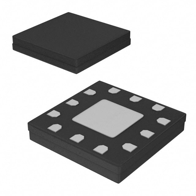 |
| 产品型号 | HMC774LC3B |
| RF类型 | 通用 |
| rohs | 无铅 / 符合限制有害物质指令(RoHS)规范要求 |
| 产品系列 | - |
| 供应商器件封装 | 12-CSMT (3x3) |
| 其它名称 | 1127-1723 |
| 包装 | 剪带 |
| 噪声系数 | - |
| 增益 | - |
| 封装/外壳 | 12-VFCQFN 裸露焊盘 |
| 标准包装 | 5 |
| 混频器数 | 1 |
| 电压-电源 | - |
| 电流-电源 | - |
| 辅助属性 | 升/降频器 |
| 配用 | /product-detail/zh/125042-HMC774LC3B/1127-2412-ND/4794704 |
| 频率 | 7GHz ~ 34GHz |
Datasheet
PDF Datasheet 数据手册内容提取
HMC774LC3B v01.0514 GaAs MMIC FUNDAMENTAL MIXER, 7 - 34 GHz Typical Applications Features The HMC774LC3B is ideal for: Passive: No DC Bias Required T • Point-to-Point Radios Input IP3: +22 dBm M • Point-to-Multi-Point Radios & VSAT LO/RF Isolation: 35 dB S • Test Equipment & Sensors Wide IF Bandwidth: DC - 8 GHz - D • Military End-Use 12 Lead Ceramic 3x3 mm SMT Package: 9mm2 E C N A Functional Diagram General Description L A The HMC774LC3B is a general purpose double B balanced mixer in a leadless RoHS compliant SMT E package that can be used as an upconverter or L downconverter between 7 and 34 GHz. This mixer B requires no external components or matching U circuitry. The HMC774LC3B provides excellent LO to O RF and LO to IF suppression due to optimized balun D structures. The mixer operates best with LO drive & levels above +15 dBm. The HMC774LC3B eliminates the need for wire bonding, allowing use of surface E L mount manufacturing techniques. G N I S - S R E Electrical Specifications, T = +25° C, IF = 0.5 GHz, LO = +15 dBm* X A I M Parameter Min. Typ. Max. Min. Typ. Max. Units Frequency Range, RF & LO 7 - 20 20 - 34 GHz Frequency Range, IF DC - 8 DC - 8 GHz Conversion Loss 10 13 11 14 dB LO to RF Isolation 35 35 dB LO to IF Isolation 20 30 25 40 dB RF to IF Isolation 7 10 14 20 dB IP3 (Input) 20 22 dBm IP2 (Input) 45 48 dBm 1 dB Gain Compression (Input) 12 13 dBm *Unless otherwise noted, all measurements performed as downconverter, IF = 0.5 GHz. InFfoormra tpiorni cfuern,is hdeed lbivy eArnyal oag nDdev itcoes pisl abcelieev eodr dto ebres a: cHcuirtatteit ean dM reicliarbolew. Haovweev eCr, onor poFroart ipornic,e 2, dEelliivzearby,e atnhd D tor ivpela,c eC horedlemrss: fAonradlo, gM DAe v0ic1e8s2, 4Inc., responsibility is assumed by Analog Devices for its use, nor for any infringements of patents or other One Technology Way, P.O. Box 9106, Norwood, MA 02062-9106 1 rliicgehntss eo fi sth girrda nptaerdti ebsy t himatp mlicPaayht ioroens nuolret of:rto hm9er 7wits8is ue-s 2eu.n5 dS0epre- ca3infi3yc ap4tiao3tne sn ts ou rb Fjpeaactte xtno:t cr9higa7hnt8gs e-o 2wf Ai5thn0oaulo-t g3n oD3tiec7vei3.c eN s o. OPrhdoneer: O78n1--3li2n9e- 4a7t0 0w (cid:127)w Owrd.ehri totnitlein.ec aot mwww.analog.com Trademarks and registered trademarks aArep thpe lpircopaetrityo onf thSeiur rpesppeoctrivte: oPwhneorsn.e: 978-250-33A4p3p l icoart i oanp Spusp@pohrti:t Ptihteon.ceo: 1m-800-ANALOG-D
HMC774LC3B v01.0514 GaAs MMIC FUNDAMENTAL MIXER, 7 - 34 GHz Conversion Gain vs. Temperature Isolation -4 0 T -10 B) M d -8 N GAIN ( ON (dB) -20 LLROOF///RIIFFF S SIO -12 ATI -30 - R L D E O NV +25 C IS -40 E O -16 +85 C C -40 C C -50 N -20 -60 A 6 11 16 21 26 31 36 6 11 16 21 26 31 36 L RF FREQUENCY (GHz) FREQUENCY (GHz) A B E Conversion Gain vs. LO Drive Return Loss L B 0 0 U RF LO O B) N (d -10 dB) -5 D N GAI OSS ( & CONVERSIO --3200 111135 dddBBBmmm RETURN L --1150 GLE 17 dBm N -40 -20 SI 6 11 16 21 26 31 36 6 11 16 21 26 31 36 RF FREQUENCY (GHz) FREQUENCY (GHz) - S R Upconverter Performance E IF Bandwidth Conversion Gain vs. LO Drive X 0 0 I M -5 -5 B) d E (dB) -10 GAIN ( -10 S N N O -15 RESPO --2105 Conversion Gain CONVERSI -20 111 9135 ddddBBBBmmmm IF Return Loss -25 17 dBm -25 -30 0 2 4 6 8 10 12 6 11 16 21 26 31 36 IF FREQUENCY (GHz) RF FREQUENCY (GHz) InFfoormra tpiorni cfuern,is hdeed lbivy eArnyal oag nDdev itcoes pisl abcelieev eodr dto ebres a: cHcuirtatteit ean dM reicliarbolew. Haovweev eCr, onor poFroart ipornic,e 2, dEelliivzearby,e atnhd D tor ivpela,c eC horedlemrss: fAonradlo, gM DAe v0ic1e8s2, 4Inc., responsibility is assumed by Analog Devices for its use, nor for any infringements of patents or other One Technology Way, P.O. Box 9106, Norwood, MA 02062-9106 rights of third parties that mPayh roesnulet f:ro m9 7its8 u-s2e.5 S0pe-c3ifi3ca4tio3n s s u bFjeact xto: c9ha7n8ge- 2wi5th0ou-t 3no3tic7e3. N o OPrhdoneer: O78n1--3li2n9e- 4a7t0 0w (cid:127)w Owrd.ehri totnitlein.ec aot mwww.analog.com 2 license is granted by implication or otherwise under any patent or patent rights of Analog Devices. Trademarks and registered trademarks aArep thpe lpircopaetrityo onf thSeiur rpesppeoctrivte: oPwhneorsn.e: 978-250-33A4p3p l icoart i oanp Spusp@pohrti:t Ptihteon.ceo: 1m-800-ANALOG-D
HMC774LC3B v01.0514 GaAs MMIC FUNDAMENTAL MIXER, 7 - 34 GHz Input IP3 vs. LO Drive [1] Input IP3 vs. Temperature [1] 35 35 T 30 30 M 25 25 S Bm) 20 Bm) 20 D - IP3 (d 15 IP3 (d 15 +25 C +85 C E 10 11 dBm 10 -40 C C 13 dBm 15 dBm 5 17 dBm 5 N A 0 0 6 11 16 21 26 31 36 6 11 16 21 26 31 36 L RF FREQUENCY (GHz) RF FREQUENCY (GHz) A B E L Input IP2 vs. LO Drive [1] Input IP2 vs. Temperature [1] B 70 70 U O 60 60 D 50 50 & Bm) Bm) E P2 (d 40 P2 (d 40 I I L 30 30 +25 C G 11 dBm +85 C N 20 1135 ddBBmm 20 -40 C 17 dBm SI 10 10 6 11 16 21 26 31 36 6 11 16 21 26 31 36 - RF FREQUENCY (GHz) RF FREQUENCY (GHz) S R E Input P1dB vs. Temperature MxN Spurious Outputs X MI 22 nLO mRF 0 1 2 3 4 18 0 xx 10 39 xx xx Bm) 14 1 5 0 37 43 xx B (d 2 30 49 47 55 68 P1d 10 3 xx 74 62 45 63 4 xx xx xx 77 71 +25 C 6 +85 C RF = 17.5 GHz @ -10 dBm -40 C LO = 18 GHz @ +15 dBm All values in dBc below the IF output power level. 2 6 11 16 21 26 31 36 RF FREQUENCY (GHz) [1] Two-tone input power = -10 dBm each tone, 1 MHz spacing. InFfoormra tpiorni cfuern,is hdeed lbivy eArnyal oag nDdev itcoes pisl abcelieev eodr dto ebres a: cHcuirtatteit ean dM reicliarbolew. Haovweev eCr, onor poFroart ipornic,e 2, dEelliivzearby,e atnhd D tor ivpela,c eC horedlemrss: fAonradlo, gM DAe v0ic1e8s2, 4Inc., responsibility is assumed by Analog Devices for its use, nor for any infringements of patents or other One Technology Way, P.O. Box 9106, Norwood, MA 02062-9106 3 rliicgehntss eo fi sth girrda nptaerdti ebsy t himatp mlicPaayht ioroens nuolret of:rto hm9er 7wits8is ue-s 2eu.n5 dS0epre- ca3infi3yc ap4tiao3tne sn ts ou rb Fjpeaactte xtno:t cr9higa7hnt8gs e-o 2wf Ai5thn0oaulo-t g3n oD3tiec7vei3.c eN s o. OPrhdoneer: O78n1--3li2n9e- 4a7t0 0w (cid:127)w Owrd.ehri totnitlein.ec aot mwww.analog.com Trademarks and registered trademarks aArep thpe lpircopaetrityo onf thSeiur rpesppeoctrivte: oPwhneorsn.e: 978-250-33A4p3p l icoart i oanp Spusp@pohrti:t Ptihteon.ceo: 1m-800-ANALOG-D
HMC774LC3B v01.0514 GaAs MMIC FUNDAMENTAL MIXER, 7 - 34 GHz Absolute Maximum Ratings RF / IF Input +21 dBm ELECTROSTATIC SENSITIVE DEVICE LO Drive +27 dBm T OBSERVE HANDLING PRECAUTIONS Channel Temperature 150 °C M Continuous Pdiss (Ta = 85 °C) S 189 mW (derate 2.9 mW/°C above 85 °C) - Thermal Resistance 343 °C/W D (channel to ground paddle) E Storage Temperature -65 to +150 °C C Operating Temperature -40 to +85 °C N A L A B Outline Drawing E L B U O D & E L G N I S - S R NOTES: E 1. PACKAGE BODY MATERIAL: ALUMINA. X 2. LEAD AND GROUND PADDLE PLATING: GOLD FLASH OVER NICKEL. 3. DIMENSIONS ARE IN INCHES (MILLIMETERS). I M 4. LEAD SPACING TOLERANCE IS NON-CUMULATIVE. 5. CHARACTERS TO BE HELVETICA MEDIUM, .025 HIGH, BLACK INK, OR LASER MARK LOCATED APPROX. AS SHOWN. 6. PACKAGE WARP SHALL NOT EXCEED 0.05MM DATUM – C – 7. ALL GROUND LEADS AND GROUND PADDLE MUST BE SOLDERED TO PCB RF GROUND. Package Information Part Number Package Body Material Lead Finish MSL Rating Package Marking [2] HMC774LC3B Alumina, White Gold over Nickel MSL3 [1] H774 XXXX [1] Max peak reflow temperature of 260 °C [2] 4-Digit lot number XXXX InFfoormra tpiorni cfuern,is hdeed lbivy eArnyal oag nDdev itcoes pisl abcelieev eodr dto ebres a: cHcuirtatteit ean dM reicliarbolew. Haovweev eCr, onor poFroart ipornic,e 2, dEelliivzearby,e atnhd D tor ivpela,c eC horedlemrss: fAonradlo, gM DAe v0ic1e8s2, 4Inc., responsibility is assumed by Analog Devices for its use, nor for any infringements of patents or other One Technology Way, P.O. Box 9106, Norwood, MA 02062-9106 rights of third parties that mPayh roesnulet f:ro m9 7its8 u-s2e.5 S0pe-c3ifi3ca4tio3n s s u bFjeact xto: c9ha7n8ge- 2wi5th0ou-t 3no3tic7e3. N o OPrhdoneer: O78n1--3li2n9e- 4a7t0 0w (cid:127)w Owrd.ehri totnitlein.ec aot mwww.analog.com 4 license is granted by implication or otherwise under any patent or patent rights of Analog Devices. Trademarks and registered trademarks aArep thpe lpircopaetrityo onf thSeiur rpesppeoctrivte: oPwhneorsn.e: 978-250-33A4p3p l icoart i oanp Spusp@pohrti:t Ptihteon.ceo: 1m-800-ANALOG-D
HMC774LC3B v01.0514 GaAs MMIC FUNDAMENTAL MIXER, 7 - 34 GHz Pin Descriptions Pin Number Function Description Interface Schematic T 1, 3, 7, 9, These pins and package bottom must M GND 10, 12 be connected to RF/DC ground. S - D This pin is DC coupled 2 LO and matched to 50 Ohms. E C N These pins are not connected internally; however, all data A 4, 6, 11 N/C shown herein was measured with these pins connected to RF/DC ground externally. L A This pin is DC coupled. For applications not requiring opera- B tion to DC, this port should be DC blocked externally using a series capacitor whose value has been chosen to pass the 5 IF E necessary IF frequency range. For operation to DC, this pin L must not source or sink more than 2 mA of current or part non-function and possible part failure will result. B U O This pin is DC coupled 8 RF D and matched to 50 Ohms. & E L G N I S - S R E X I M InFfoormra tpiorni cfuern,is hdeed lbivy eArnyal oag nDdev itcoes pisl abcelieev eodr dto ebres a: cHcuirtatteit ean dM reicliarbolew. Haovweev eCr, onor poFroart ipornic,e 2, dEelliivzearby,e atnhd D tor ivpela,c eC horedlemrss: fAonradlo, gM DAe v0ic1e8s2, 4Inc., responsibility is assumed by Analog Devices for its use, nor for any infringements of patents or other One Technology Way, P.O. Box 9106, Norwood, MA 02062-9106 5 rliicgehntss eo fi sth girrda nptaerdti ebsy t himatp mlicPaayht ioroens nuolret of:rto hm9er 7wits8is ue-s 2eu.n5 dS0epre- ca3infi3yc ap4tiao3tne sn ts ou rb Fjpeaactte xtno:t cr9higa7hnt8gs e-o 2wf Ai5thn0oaulo-t g3n oD3tiec7vei3.c eN s o. OPrhdoneer: O78n1--3li2n9e- 4a7t0 0w (cid:127)w Owrd.ehri totnitlein.ec aot mwww.analog.com Trademarks and registered trademarks aArep thpe lpircopaetrityo onf thSeiur rpesppeoctrivte: oPwhneorsn.e: 978-250-33A4p3p l icoart i oanp Spusp@pohrti:t Ptihteon.ceo: 1m-800-ANALOG-D
HMC774LC3B v01.0514 GaAs MMIC FUNDAMENTAL MIXER, 7 - 34 GHz Evaluation PCB T M S - D E C N A L A B E L B U O D & E L G N I S - S R E List of Materials for Evaluation PCB 125042 [1] X The circuit board used in this application should use I Item Description M RF circuit design techniques. Signal lines should J1 - J2 Southwest K Connector have 50 Ohm impedance while the package ground J3 Johnson SMA Connector leads and exposed paddle should be connected U1 HMC774LC3B Mixer directly to the ground plane similar to that shown. PCB [2] 125040 Evaluation PCB A sufficient number of via holes should be used to [1] Reference this number when ordering compete evaluation PCB connect the top and bottom ground planes. The [2] Circuit Board Material: Arlon 25FR or Rogers 4350 evaluation board should be mounted to an appro- priate heat sink. The evaluation circuit board shown is available from Hittite upon request. InFfoormra tpiorni cfuern,is hdeed lbivy eArnyal oag nDdev itcoes pisl abcelieev eodr dto ebres a: cHcuirtatteit ean dM reicliarbolew. Haovweev eCr, onor poFroart ipornic,e 2, dEelliivzearby,e atnhd D tor ivpela,c eC horedlemrss: fAonradlo, gM DAe v0ic1e8s2, 4Inc., responsibility is assumed by Analog Devices for its use, nor for any infringements of patents or other One Technology Way, P.O. Box 9106, Norwood, MA 02062-9106 rights of third parties that mPayh roesnulet f:ro m9 7its8 u-s2e.5 S0pe-c3ifi3ca4tio3n s s u bFjeact xto: c9ha7n8ge- 2wi5th0ou-t 3no3tic7e3. N o OPrhdoneer: O78n1--3li2n9e- 4a7t0 0w (cid:127)w Owrd.ehri totnitlein.ec aot mwww.analog.com 6 license is granted by implication or otherwise under any patent or patent rights of Analog Devices. Trademarks and registered trademarks aArep thpe lpircopaetrityo onf thSeiur rpesppeoctrivte: oPwhneorsn.e: 978-250-33A4p3p l icoart i oanp Spusp@pohrti:t Ptihteon.ceo: 1m-800-ANALOG-D