首页 > HMC713MS8E > 详情
 Datasheet下载
- 型号: HMC713MS8E
- 制造商: Hittite
- 库位|库存: xxxx|xxxx
- 要求:
| 数量阶梯 | 香港交货 | 国内含税 |
| +xxxx | $xxxx | ¥xxxx |
查看当月历史价格
查看今年历史价格
产品参数
| 参数 | 数值 |
| 产品目录 | 射频/IF 和 RFID |
| 描述 | RF LOG DETECT CNTRL 2.7GHZ 8MSOP |
| 产品分类 | RF 检测器 |
| 品牌 | Hittite Microwave Corporation |
| 数据手册 | 点击此处下载产品Datasheet |
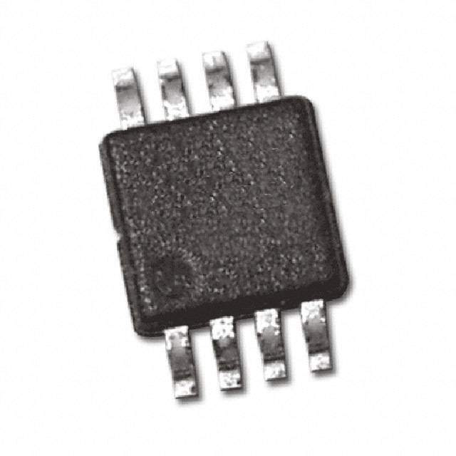
| 产品图片 |  |
| 产品型号 | HMC713MS8E |
| RF类型 | 通用 |
| rohs | 无铅 / 符合限制有害物质指令(RoHS)规范要求 |
| 产品系列 | - |
| 其它名称 | 1127-1179-1 |
| 包装 | 剪切带 (CT) |
| 封装/外壳 | 8-TSSOP,8-MSOP(0.118",3.00mm 宽) |
| 标准包装 | 1 |
| 电压-电源 | 2.7 V ~ 5.5 V |
| 电流-电源 | 17mA |
| 精度 | ±1dB |
| 输入范围 | - |
| 频率 | 45MHz ~ 2.7GHz |
Datasheet
PDF Datasheet 数据手册内容提取
HMC713MS8 / 713MS8E v06.0412 54 dB, LOGARITHMIC DETECTOR / CONTROLLER, 45 - 2700 MHz Typical Applications Features the HMc713Ms8(e) is ideal for: wide Dynamic range: up to 54 dB t • Cellular Infrastructure High Accuracy: M ±1 dB with 54 dB range Up to 2.7 GHz • WiMAX, WiBro & LTE/4G s Fast output response time • Power Monitoring & Control Circuitry - supply Voltage: +2.7 to +5.5V • Receiver Signal Strength Indication (RSSI) s Power-Down Mode r • Automatic Gain & Power Control excellent stability over temperature o • Military, ECM & Radar t MsoP-8 sMt Package: 14.8 mm² c e Functional Diagram General Description t e the HMc713Ms8(e) Logarithmic Detector/control- D ler is ideal for converting rF signals with frequencies r in the 45 MHz to 2700 MHz range, to a proportional e Dc voltage at its output. the HMc713Ms8(e) employs w a successive compression technology which delivers 54 dB of dynamic range with high conversion accuracy o over a wide input frequency range. As the input signal is P increased, successive amplifiers move into saturation one by one creating an accurate approximation of the logarithm function. the outputs of a series of detectors are summed, converted into voltage domain and buffered to drive the oUt output. For detection mode, the oUt pin is connected to the Vset input and will provide a nominal logarithmic slope of 17 mV/dB and an intercept of -68 dBm. the HMc713Ms8(e) can also be used in the controller mode where an external voltage is applied to the Vset pin to create an AGc or APc feedback loop. Electrical Specifications, T = +25 °C, Vcc= +3V [1] A Parameter typ. typ. typ. typ. typ. typ. Units Input Frequency 45 100 900 1900 2200 2700 MHz ±3 dB Dynamic range 60 61 61 62 62 68 dB ±3 dB Dynamic range center -26 -28 -28 -30 -31 -27 dBm ±1 dB Dynamic range 53 54 54 54 53 59 dB oUt slope 17.3 17.3 17.2 17.1 17.1 17.2 mV/dB OUT Intercept -68 -68 -69 -71 -72 -70 dBm Variation of oUt with temperature -0.8 -1 -0.9 -0.5 -0.6 -0.5 dB from -40°C to +85°C @ -20 dBm Input [1] Detector mode measurements; oUt (Pin 6) is shorted to Vset (Pin 3) through an rc network. InFfoormra tpiorni cfuern,is hdeed lbivy eArnyal oag nDdev itcoes pisl abcelieev eodr dto ebres a: cHcuirtatteit ean dM reicliarbolew. Haovweev eCr, onor poFroart ipornic,e 2, dEelliivzearby,e atnhd D tor ivpela,c eC horedlemrss: fAonradl,o gM DAe v0ic1e8s2, 4Inc., responsibility is assumed by Analog Devices for its use, nor for any infringements of patents or other One Technology Way, P.O. Box 9106, Norwood, MA 02062-9106 1 rliicgehntss eo fi sth girrda nptaerdti ebsy t himatp mlicPaayht ioroens nuolret of:rto hm9er 7wits8is ue-s 2eu.n5 dS0epre- ca3infi3yc ap4tiao3tne sn ts ou rb Fjpeaactte xtno:t cr9higa7hnt8gs e-o 2wf Ai5thn0oaulo-t g3n oD3tiec7vei3.c eN s o. OPrhdoneer: O78n1--3li2n9e- 4a7t0 0w (cid:127)w Owrd.ehri totnitlein.ec aot mwww.analog.com Trademarks and registered trademarks aArep thpe lpircopaetrityo onf thSeiur rpesppeoctrivte: oPwhneorsn.e: 978-250-33A4p3p l icoart i oanp Spusp@pohrti:t Ptihteo.nceo: 1m-800-ANALOG-D
HMC713MS8 / 713MS8E v06.0412 54 DB, LOGARITHMIC DETECTOR / CONTROLLER, 45 - 2700 MHz Electrical Specifications, (continued) Parameter conditions Min. typ. Max. Units Power Down (EN) Interface t Voltage range for Normal Mode 0.8 x Vcc V M Voltage range for Powerdown Mode 0.2 x Vcc V s threshold Voltage Vcc/2 V - Power Supply (Vcc) s operating Voltage range 2.7 - 5.5 V r supply current in Normal Mode 17 mA o supply current in Power Down Mode 0.3 mA t OUT Interface c rise time cLPF= 0, No Power to -10 dBm, 10% - 90% 24 ns e Fall time cLPF= 0, -10 dBm to No Power, 90% - 10% 70 ns t 3 dB reduction in output Video Bw 16 MHz e demodulated output voltage D Voltage range closed Loop (eval Board setup) 0.2 - 1.2 V 0.1 to (Vcc r Voltage range open Loop V -0.1) e current Drive source / sink 3.5 / 0.51 mA w OUTN Interface o current Drive source / sink 3.6 / 0.47 mA OUTN Interface P output Voltage range 0.2 - 2.1 V RF Input F= 50 MHz to 2.5 GHz Input Return Loss (S11) 10 dB Z0= 50Ω, see plot VSET Interface Input Impedance 1 MΩ Input Voltage Range eval Board 0.2 - 1.2 V Low Frequency Gain Vset to oUt 64 dB open Loop corner Frequency 11 kHz InFfoormra tpiorni cfuern,is hdeed lbivy eArnyal oag nDdev itcoes pisl abcelieev eodr dto ebres a: cHcuirtatteit ean dM reicliarbolew. Haovweev eCr, onor poFroart ipornic,e 2, dEelliivzearby,e atnhd D tor ivpela,c eC horedlemrss: fAonradl,o gM DAe v0ic1e8s2, 4Inc., responsibility is assumed by Analog Devices for its use, nor for any infringements of patents or other One Technology Way, P.O. Box 9106, Norwood, MA 02062-9106 rights of third parties that mPayh roesnulet f:ro m9 7its8 u-s2e.5 S0pe-c3ifi3ca4tio3n s s u bFjeact xto: c9ha7n8ge- 2wi5th0ou-t 3no3tic7e3. N o OPrhdoneer: O78n1--3li2n9e- 4a7t0 0w (cid:127)w Owrd.ehri totnitlein.ec aot mwww.analog.com 2 license is granted by implication or otherwise under any patent or patent rights of Analog Devices. Trademarks and registered trademarks aArep thpe lpircopaetrityo onf thSeiur rpesppeoctrivte: oPwhneorsn.e: 978-250-33A4p3p l icoart i oanp Spusp@pohrti:t Ptihteo.nceo: 1m-800-ANALOG-D
HMC713MS8 / 713MS8E v06.0412 54 DB, LOGARITHMIC DETECTOR / CONTROLLER, 45 - 2700 MHz Output Voltage & Error Output Voltage & Error vs. Input Power, Fin = 45 MHz vs. Input Power, Fin = 100 MHz 2.4 6 2.4 6 OUT Err +25C t OUT Err +85C OUT Err +25C M 2 OOUUTT ENr rE -r4r 0+C25C 4 2 OOOUUUTTT EENrr rrE +r-r48 +052CC5C 4 OUT N Err +85C OUT N Err +85C rs - s OUT, OUTN (V) 011...826 OUT N Err -40C -022 ERROR (dB) OUT, OUTN (V)011...826 OUT N Err -40C -022 ERROR (dB) o 0.4 OUT -4 0.4 OUT OUT N -4 OUT N t c 0 -6 0 -6 e -60 -50 -40 -30 -20 -10 0 10 -60 -50 -40 -30 -20 -10 0 10 INPUT POWER (dBm) INPUT POWER (dBm) t e D Output Voltage & Error Output Voltage & Error r vs. Input Power, Fin = 900 MHz vs. Input Power, Fin = 1900 MHz e 2.4 6 2.4 6 w OUT Err +25C OUT Err +25C o 2 OOUUTT EErrrr +-4805CC 4 2 OOUUTT EErrrr +-4805CC 4 OUT N Err +25C OUT N Err +25C P V)1.6 OOUUTT NN EErrrr +-4805CC 2 V)1.6 OOUUTT NN EErrrr +-4805CC 2 N ( ER N ( ER OUT, OUT01..82 -02 ROR (dB) OUT, OUT01..82 -02 ROR (dB) OUT OUT 0.4 OUT N -4 0.4 OUT N -4 0 -6 0 -6 -60 -50 -40 -30 -20 -10 0 10 -60 -50 -40 -30 -20 -10 0 10 Input Power (dBm) INPUT POWER (dBm) Output Voltage & Error Output Voltage & Error vs. Input Power, Fin = 2200 MHz vs. Input Power, Fin = 2700 MHz 2.4 6 2.4 6 OUT Err +25C 2 OOUUTT EErrrr +-4805CC 4 2 OOUUTT EErrrr ++2855CC 4 OUT N Err +25C OUT Err -40C OUT, OUTN (V)011...826 OOUUTT NN EErrrr +-4805CC -022 ERROR (dB) OUT, OUTN (V)011...826 OOOUUUTTT NNN EEErrrrrr ++-428055CCC -022 ERROR (dB) OUT 0.4 OUT N -4 0.4 OUT OUT N -4 0 -6 0 -6 -60 -50 -40 -30 -20 -10 0 10 -60 -50 -40 -30 -20 -10 0 10 INPUT POWER (dBm) NPUT POWER (dBm) Unless otherwise noted: Vcc= +3V, TA = +25 °C InFfoormra tpiorni cfuern,is hdeed lbivy eArnyal oag nDdev itcoes pisl abcelieev eodr dto ebres a: cHcuirtatteit ean dM reicliarbolew. Haovweev eCr, onor poFroart ipornic,e 2, dEelliivzearby,e atnhd D tor ivpela,c eC horedlemrss: fAonradl,o gM DAe v0ic1e8s2, 4Inc., responsibility is assumed by Analog Devices for its use, nor for any infringements of patents or other One Technology Way, P.O. Box 9106, Norwood, MA 02062-9106 3 rliicgehntss eo fi sth girrda nptaerdti ebsy t himatp mlicPaayht ioroens nuolret of:rto hm9er 7wits8is ue-s 2eu.n5 dS0epre- ca3infi3yc ap4tiao3tne sn ts ou rb Fjpeaactte xtno:t cr9higa7hnt8gs e-o 2wf Ai5thn0oaulo-t g3n oD3tiec7vei3.c eN s o. OPrhdoneer: O78n1--3li2n9e- 4a7t0 0w (cid:127)w Owrd.ehri totnitlein.ec aot mwww.analog.com Trademarks and registered trademarks aArep thpe lpircopaetrityo onf thSeiur rpesppeoctrivte: oPwhneorsn.e: 978-250-33A4p3p l icoart i oanp Spusp@pohrti:t Ptihteo.nceo: 1m-800-ANALOG-D
HMC713MS8 / 713MS8E v06.0412 54 DB, LOGARITHMIC DETECTOR / CONTROLLER, 45 - 2700 MHz OUT Slope vs. Frequency OUT Slope vs. Supply Voltage 20 20 19 ++ -284550CCC ssslllooopppeee 19 000...0194GG5HHGzzHz Mt 1.9GHz OPE (mV/dB) 1178 OPE (mV/dB) 1178 22..27GGHHzz s - s SL 16 SL r 16 o 15 t 14 15 c 0 0.3 0.6 0.9 1.2 1.5 1.8 2.1 2.4 2.7 2.7 3.1 3.5 3.9 4.3 4.7 5.1 5.5 e FREQUENCY (GHz) VOLTAGE SUPPLY (V) t e D OUT Intercept vs. Frequency OUT Intercept vs. Supply Voltage r -50 -50 e w -60 -60 o INTERCEPT (dBm)--8700 +25C intercept INTERCEPT (dBm)--8700 0001....01994GGG5HHHGzzzHz P -90 +85C intercept -90 2.2GHz -40C intercept 2.7GHz -100 -100 0 0.3 0.6 0.9 1.2 1.5 1.8 2.1 2.4 2.7 2.7 3.1 3.5 3.9 4.3 4.7 5.1 5.5 FREQUENCY (GHz) VOLTAGE SUPPLY (V) OUT vs. Frequency & Input Power OUT Voltage & Error vs. Frequency 1.4 1.8 6 0dBm 1.2 1.5 4 -10dBm 1 -20dBm 1.2 2 UT (V) 0.8 -30dBm T (V)0.9 Error 0 ERRO O 0.6 U R 0.4 -40dBm O0.6 OUT -2 (dB) -50dBm 0.045GHz 0.1GHz 0.2 0.3 01..99GGHHzz -4 -60dBm 22..27GGHHzz 0 0 -6 0 0.3 0.6 0.9 1.2 1.5 1.8 2.1 2.4 2.7 -60 -50 -40 -30 -20 -10 0 10 FREQUENCY (GHz) INPUT POWER (dBm) Unless otherwise noted: Vcc= +3V, TA = +25 °C InFfoormra tpiorni cfuern,is hdeed lbivy eArnyal oag nDdev itcoes pisl abcelieev eodr dto ebres a: cHcuirtatteit ean dM reicliarbolew. Haovweev eCr, onor poFroart ipornic,e 2, dEelliivzearby,e atnhd D tor ivpela,c eC horedlemrss: fAonradl,o gM DAe v0ic1e8s2, 4Inc., responsibility is assumed by Analog Devices for its use, nor for any infringements of patents or other One Technology Way, P.O. Box 9106, Norwood, MA 02062-9106 rights of third parties that mPayh roesnulet f:ro m9 7its8 u-s2e.5 S0pe-c3ifi3ca4tio3n s s u bFjeact xto: c9ha7n8ge- 2wi5th0ou-t 3no3tic7e3. N o OPrhdoneer: O78n1--3li2n9e- 4a7t0 0w (cid:127)w Owrd.ehri totnitlein.ec aot mwww.analog.com 4 license is granted by implication or otherwise under any patent or patent rights of Analog Devices. Trademarks and registered trademarks aArep thpe lpircopaetrityo onf thSeiur rpesppeoctrivte: oPwhneorsn.e: 978-250-33A4p3p l icoart i oanp Spusp@pohrti:t Ptihteo.nceo: 1m-800-ANALOG-D
HMC713MS8 / 713MS8E v06.0412 54 DB, LOGARITHMIC DETECTOR / CONTROLLER, 45 - 2700 MHz Output Response Output Response Fall Time @ 900 MHz, C1 = Open Fall Time @ 900 MHz, C1 = 10nF 1.5 1.5 t 0dBm 0dBm M 1.2 --1200ddBBmm 1.2 --1200ddBBmm -30dBm -30dBm s - T (V) 0.9 T (V) 0.9 U U s O 0.6 O 0.6 r o 0.3 0.3 t c 0 0 0 50 100 150 200 250 300 350 400 450 500 0 25 50 75 100 125 150 175 200 e TIME (ns) TIME (us) t e D Output Response Output Response r Rise Time @ 900 MHz, C1 = Open Rise Time @ 900 MHz, C1 = 10nF e 1.5 1.5 w 0dBm 0dBm -10dBm -10dBm o 1.2 -20dBm 1.2 -20dBm -30dBm -30dBm P V) 0.9 V) 0.9 T ( T ( U U O O 0.6 0.6 0.3 0.3 0 0 0 50 100 150 200 250 300 350 400 450 500 0 10 20 30 40 50 60 70 80 90 100 TIME (ns) TIME (us) Input Return Loss 0 -10 B) d SS (-20 O L N UR-30 T E R -40 -50 0 0.5 1 1.5 2 2.5 3 FREQUENCY (GHz) Unless otherwise noted: Vcc= +3V, TA = +25 °C InFfoormra tpiorni cfuern,is hdeed lbivy eArnyal oag nDdev itcoes pisl abcelieev eodr dto ebres a: cHcuirtatteit ean dM reicliarbolew. Haovweev eCr, onor poFroart ipornic,e 2, dEelliivzearby,e atnhd D tor ivpela,c eC horedlemrss: fAonradl,o gM DAe v0ic1e8s2, 4Inc., responsibility is assumed by Analog Devices for its use, nor for any infringements of patents or other One Technology Way, P.O. Box 9106, Norwood, MA 02062-9106 5 rliicgehntss eo fi sth girrda nptaerdti ebsy t himatp mlicPaayht ioroens nuolret of:rto hm9er 7wits8is ue-s 2eu.n5 dS0epre- ca3infi3yc ap4tiao3tne sn ts ou rb Fjpeaactte xtno:t cr9higa7hnt8gs e-o 2wf Ai5thn0oaulo-t g3n oD3tiec7vei3.c eN s o. OPrhdoneer: O78n1--3li2n9e- 4a7t0 0w (cid:127)w Owrd.ehri totnitlein.ec aot mwww.analog.com Trademarks and registered trademarks aArep thpe lpircopaetrityo onf thSeiur rpesppeoctrivte: oPwhneorsn.e: 978-250-33A4p3p l icoart i oanp Spusp@pohrti:t Ptihteo.nceo: 1m-800-ANALOG-D
HMC713MS8 / 713MS8E v06.0412 54 DB, LOGARITHMIC DETECTOR / CONTROLLER, 45 - 2700 MHz Absolute Maximum Ratings Vcc 0 to +5.6V ELECTROSTATIC SENSITIVE DEVICE eN 0 to +5.6V t OBSERVE HANDLING PRECAUTIONS Vset 0 to +5.6V M oUt output current 5 mA s oUtN output current 5 mA - RF Input Power 12 dBm s Junction temperature 125 °c r continuous Pdiss (t = 85°c) o 0.22 watts (Derate 5.43 mw/°c above 85°c) t thermal resistance (rth) 184 °c/w c (junction to lead) e storage temperature -65 to +150 °c t operating temperature -40 to +85 °c e esD sensitivity (HBM) class 1c D Outline Drawing r e w o P Notes: 1. PACKAGE BODY MATERIAL: LOW STRESS INJECTION MOLDED PLASTIC SILICA AND SILICON IMPREGNATED. 2. LEAD MATERIAL: COPPER ALLOY 3. LEAD PLATING: 100% MATTE TIN 4. DIMENSIONS ARE IN INCHES [MILLIMETERS]. 5. DIMENSION DOES NOT INCLUDE MOLDFLASH OF 0.15mm PER SIDE. 6. DIMENSION DOES NOT INCLUDE MOLDFLASH OF 0.25mm PER SIDE. 7. ALL GroUND LeADs MUst Be soLDereD to PcB rF GroUND. Package Information Part Number Package Body Material Lead Finish MsL rating Package Marking [3] HMc713Ms8 Low Stress Injection Molded Plastic sn/Pb solder MsL1 [1] H713 XXXX HMc713Ms8e RoHS-compliant Low Stress Injection Molded Plastic 100% matte sn MsL1 [2] H713 XXXX [1] Max peak reflow temperature of 235 °c [2] Max peak reflow temperature of 260 °c [3] 4-Digit lot number XXXX InFfoormra tpiorni cfuern,is hdeed lbivy eArnyal oag nDdev itcoes pisl abcelieev eodr dto ebres a: cHcuirtatteit ean dM reicliarbolew. Haovweev eCr, onor poFroart ipornic,e 2, dEelliivzearby,e atnhd D tor ivpela,c eC horedlemrss: fAonradl,o gM DAe v0ic1e8s2, 4Inc., responsibility is assumed by Analog Devices for its use, nor for any infringements of patents or other One Technology Way, P.O. Box 9106, Norwood, MA 02062-9106 rights of third parties that mPayh roesnulet f:ro m9 7its8 u-s2e.5 S0pe-c3ifi3ca4tio3n s s u bFjeact xto: c9ha7n8ge- 2wi5th0ou-t 3no3tic7e3. N o OPrhdoneer: O78n1--3li2n9e- 4a7t0 0w (cid:127)w Owrd.ehri totnitlein.ec aot mwww.analog.com 6 license is granted by implication or otherwise under any patent or patent rights of Analog Devices. Trademarks and registered trademarks aArep thpe lpircopaetrityo onf thSeiur rpesppeoctrivte: oPwhneorsn.e: 978-250-33A4p3p l icoart i oanp Spusp@pohrti:t Ptihteo.nceo: 1m-800-ANALOG-D
HMC713MS8 / 713MS8E v06.0412 54 DB, LOGARITHMIC DETECTOR / CONTROLLER, 45 - 2700 MHz Pin Descriptions Pin Number Function Description Interface Schematic t M s - s 1 INP rF input pin. r o t c e t e enable pin. D Apply VeN >0.8 x Vcc for normal operation. Apply VeN <0.2xVcc to disable the HMc713Ms8e and r reduce supply current to 0.3mA. 2 eN e to ensure proper start-up apply the power-up sequence w shown in the “Power-Up timing Diagram” attached to the application circuit. o P set point input for controller mode. 3 Vset connect to oUt with the resistor network shown in evaluation board drawing for detector mode. connection for ground referenced external lowpass 4 cLPF filter capacitor. 5 GND Device ground. InFfoormra tpiorni cfuern,is hdeed lbivy eArnyal oag nDdev itcoes pisl abcelieev eodr dto ebres a: cHcuirtatteit ean dM reicliarbolew. Haovweev eCr, onor poFroart ipornic,e 2, dEelliivzearby,e atnhd D tor ivpela,c eC horedlemrss: fAonradl,o gM DAe v0ic1e8s2, 4Inc., responsibility is assumed by Analog Devices for its use, nor for any infringements of patents or other One Technology Way, P.O. Box 9106, Norwood, MA 02062-9106 7 rliicgehntss eo fi sth girrda nptaerdti ebsy t himatp mlicPaayht ioroens nuolret of:rto hm9er 7wits8is ue-s 2eu.n5 dS0epre- ca3infi3yc ap4tiao3tne sn ts ou rb Fjpeaactte xtno:t cr9higa7hnt8gs e-o 2wf Ai5thn0oaulo-t g3n oD3tiec7vei3.c eN s o. OPrhdoneer: O78n1--3li2n9e- 4a7t0 0w (cid:127)w Owrd.ehri totnitlein.ec aot mwww.analog.com Trademarks and registered trademarks aArep thpe lpircopaetrityo onf thSeiur rpesppeoctrivte: oPwhneorsn.e: 978-250-33A4p3p l icoart i oanp Spusp@pohrti:t Ptihteo.nceo: 1m-800-ANALOG-D
HMC713MS8 / 713MS8E v06.0412 54 DB, LOGARITHMIC DETECTOR / CONTROLLER, 45 - 2700 MHz Pin Descriptions (Continued) Pin Number Function Description Interface Schematic t M s Logarithmic output that converts the input power to a 6 oUt Dc level in controller mode. output voltage increases - with increasing amplitude s r o t c e t e Inverted logarithmic output. D 7 oUtN oUtN= 2.55 - 2 x oUt r e w o P Bias supply. 8 Vcc connect supply voltage to all this pin with appropriate filtering. InFfoormra tpiorni cfuern,is hdeed lbivy eArnyal oag nDdev itcoes pisl abcelieev eodr dto ebres a: cHcuirtatteit ean dM reicliarbolew. Haovweev eCr, onor poFroart ipornic,e 2, dEelliivzearby,e atnhd D tor ivpela,c eC horedlemrss: fAonradl,o gM DAe v0ic1e8s2, 4Inc., responsibility is assumed by Analog Devices for its use, nor for any infringements of patents or other One Technology Way, P.O. Box 9106, Norwood, MA 02062-9106 rights of third parties that mPayh roesnulet f:ro m9 7its8 u-s2e.5 S0pe-c3ifi3ca4tio3n s s u bFjeact xto: c9ha7n8ge- 2wi5th0ou-t 3no3tic7e3. N o OPrhdoneer: O78n1--3li2n9e- 4a7t0 0w (cid:127)w Owrd.ehri totnitlein.ec aot mwww.analog.com 8 license is granted by implication or otherwise under any patent or patent rights of Analog Devices. Trademarks and registered trademarks aArep thpe lpircopaetrityo onf thSeiur rpesppeoctrivte: oPwhneorsn.e: 978-250-33A4p3p l icoart i oanp Spusp@pohrti:t Ptihteo.nceo: 1m-800-ANALOG-D
HMC713MS8 / 713MS8E v06.0412 54 DB, LOGARITHMIC DETECTOR / CONTROLLER, 45 - 2700 MHz Application & Evaluation PCB Schematic t M s - s r o t c e t e D r e w o P Notes Note 1: The HMC713MS8(E) evaluation board is pre-assembled for single-ended input, and detector/RSSI mode. Note 2: For detector mode, connect high impedance volt meter to the oUt / oUtN port. Note 3: For controller mode, remove R6 & C3 and install 1k Ω resistor (R4) and 100pF capacitor (C2), then make appropriate connection to OUT and VSET. In controller mode, the OUT / OUTN output can be used to drive a variable gain amplifier, or a variable attenuator, either directly or through a buffer or microcontroller. Vset should be connected to an external supply, typically between +0.2 and +1.2V. Note 4: An external capacitance c1 can be connected to cLPF port for additional filtering of oUt and oUtN outputs.. Power-Up Timing Diagram InFfoormra tpiorni cfuern,is hdeed lbivy eArnyal oag nDdev itcoes pisl abcelieev eodr dto ebres a: cHcuirtatteit ean dM reicliarbolew. Haovweev eCr, onor poFroart ipornic,e 2, dEelliivzearby,e atnhd D tor ivpela,c eC horedlemrss: fAonradl,o gM DAe v0ic1e8s2, 4Inc., responsibility is assumed by Analog Devices for its use, nor for any infringements of patents or other One Technology Way, P.O. Box 9106, Norwood, MA 02062-9106 9 rliicgehntss eo fi sth girrda nptaerdti ebsy t himatp mlicPaayht ioroens nuolret of:rto hm9er 7wits8is ue-s 2eu.n5 dS0epre- ca3infi3yc ap4tiao3tne sn ts ou rb Fjpeaactte xtno:t cr9higa7hnt8gs e-o 2wf Ai5thn0oaulo-t g3n oD3tiec7vei3.c eN s o. OPrhdoneer: O78n1--3li2n9e- 4a7t0 0w (cid:127)w Owrd.ehri totnitlein.ec aot mwww.analog.com Trademarks and registered trademarks aArep thpe lpircopaetrityo onf thSeiur rpesppeoctrivte: oPwhneorsn.e: 978-250-33A4p3p l icoart i oanp Spusp@pohrti:t Ptihteo.nceo: 1m-800-ANALOG-D
HMC713MS8 / 713MS8E v06.0412 54 DB, LOGARITHMIC DETECTOR / CONTROLLER, 45 - 2700 MHz Evaluation PCB t M s - s r o t c e t e D r e w o P List of Materials for Evaluation PCB 121947 [1] the circuit board used in the application should Item Description use rF circuit design techniques. signal lines J1 - J3 Pc Mount sMA connector should have 50 ohm impedance while the package J5 - J7 Dc Pin ground leads and exposed paddle should be con- c3 1 pF capacitor, 0402 Pkg. nected directly to the ground plane similar to that c6 0.1 µF capacitor, 0402 Pkg. shown. A sufficient number of via holes should be r1, r7, r10 0Ω resistor, 0402 Pkg. used to connect the top and bottom ground planes. r2 51Ω resistor, 0402 Pkg. the evaluation circuit board shown is available from r3, r5 10k resistor, 0402 Pkg. Hittite upon request. r6 1k resistor, 0402 Pkg. HMc713Ms8(e) U1 Logarithmic Detector / controller PcB [2] 121944 evaluation PcB [1] reference this number when ordering complete evaluation PcB [2] circuit Board Material: Arlon 25Fr or rogers 4350 InFfoormra tpiorni cfuern,is hdeed lbivy eArnyal oag nDdev itcoes pisl abcelieev eodr dto ebres a: cHcuirtatteit ean dM reicliarbolew. Haovweev eCr, onor poFroart ipornic,e 2, dEelliivzearby,e atnhd D tor ivpela,c eC horedlemrss: fAonradl,o gM DAe v0ic1e8s2, 4Inc., responsibility is assumed by Analog Devices for its use, nor for any infringements of patents or other One Technology Way, P.O. Box 9106, Norwood, MA 02062-9106 rights of third parties that mPayh roesnulet f:ro m9 7its8 u-s2e.5 S0pe-c3ifi3ca4tio3n s s u bFjeact xto: c9ha7n8ge- 2wi5th0ou-t 3no3tic7e3. N o OPrhdoneer: O78n1--3li2n9e- 4a7t0 0w (cid:127)w Owrd.ehri totnitlein.ec aot mwww.analog.com 10 license is granted by implication or otherwise under any patent or patent rights of Analog Devices. Trademarks and registered trademarks aArep thpe lpircopaetrityo onf thSeiur rpesppeoctrivte: oPwhneorsn.e: 978-250-33A4p3p l icoart i oanp Spusp@pohrti:t Ptihteo.nceo: 1m-800-ANALOG-D