ICGOO在线商城 > 射频/IF 和 RFID > RF 放大器 > HMC708LP5E
 Datasheet下载
- 型号: HMC708LP5E
- 制造商: Hittite
- 库位|库存: xxxx|xxxx
- 要求:
| 数量阶梯 | 香港交货 | 国内含税 |
| +xxxx | $xxxx | ¥xxxx |
查看当月历史价格
查看今年历史价格
HMC708LP5E产品简介:
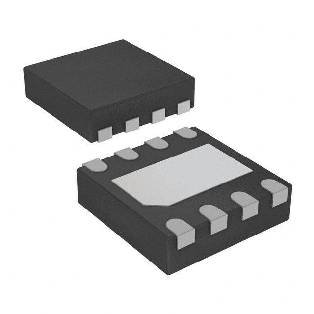
ICGOO电子元器件商城为您提供HMC708LP5E由Hittite设计生产,在icgoo商城现货销售,并且可以通过原厂、代理商等渠道进行代购。 HMC708LP5E价格参考。HittiteHMC708LP5E封装/规格:RF 放大器, RF Amplifier IC WiMAX / WiBro 1.7GHz ~ 2.2GHz 24-QFN (5x5)。您可以下载HMC708LP5E参考资料、Datasheet数据手册功能说明书,资料中有HMC708LP5E 详细功能的应用电路图电压和使用方法及教程。
| 参数 | 数值 |
| 产品目录 | |
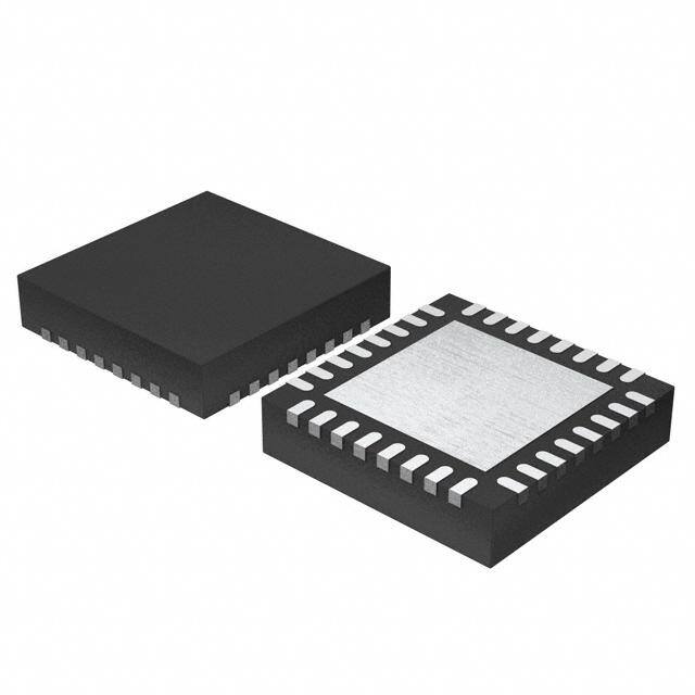
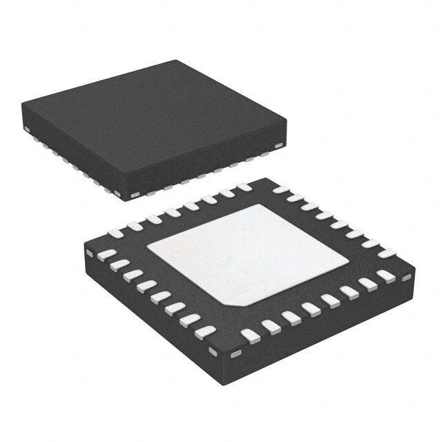
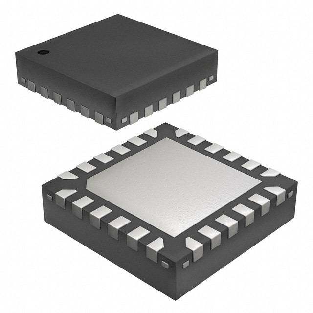
| 描述 | IC AMP DVGA LNA 6-BIT 32-QFN |
| 产品分类 | |
| 品牌 | Hittite Microwave Corporation |
| 数据手册 | |
| 产品图片 |
|
| P1dB | 21.5dBm |
| 产品型号 | HMC708LP5E |
| RF类型 | WiMAX / WiBro |
| rohs | 无铅 / 符合限制有害物质指令(RoHS)规范要求 |
| 产品系列 | - |
| 供应商器件封装 | 24-QFN(5x5) |
| 其它名称 | 1127-1540 |
| 包装 | 剪带 |
| 噪声系数 | 1dB |
| 增益 | 29dB |
| 封装/外壳 | 32-VFQFN 裸露焊盘 |
| 标准包装 | 100 |
| 测试频率 | - |
| 电压-电源 | 2.7 V ~ 3.3 V,4.5 V ~ 5.5 V |
| 电流-电源 | 97mA |
| 频率 | 1.7GHz ~ 2.2GHz |


- 商务部:美国ITC正式对集成电路等产品启动337调查
- 曝三星4nm工艺存在良率问题 高通将骁龙8 Gen1或转产台积电
- 太阳诱电将投资9.5亿元在常州建新厂生产MLCC 预计2023年完工
- 英特尔发布欧洲新工厂建设计划 深化IDM 2.0 战略
- 台积电先进制程称霸业界 有大客户加持明年业绩稳了
- 达到5530亿美元!SIA预计今年全球半导体销售额将创下新高
- 英特尔拟将自动驾驶子公司Mobileye上市 估值或超500亿美元
- 三星加码芯片和SET,合并消费电子和移动部门,撤换高东真等 CEO
- 三星电子宣布重大人事变动 还合并消费电子和移动部门
- 海关总署:前11个月进口集成电路产品价值2.52万亿元 增长14.8%


PDF Datasheet 数据手册内容提取
HMC708LP5 / 708LP5E v04.0112 0.5 dB LSB 6-BIT DIGITAL VARIABLE GAIN AMPLIFIER, 1700 - 2200 MHz Typical Applications Features The HMC708LP5(E) is ideal for: -2.5 to +29 dB Gain Control in 0.5 dB Steps • Cellular Infrastructure Power-up State Selection T M • WiBro, WiMAX and LTE/ 4G High Output IP3: +37 dBm S • Microwave Radio & VSAT Low Noise Figure: 1 dB - • Test Equipment and Sensors TTL/CMOS Compatible L Serial, Parallel, or Latched Parallel Control A ±0.25 dB Typical Step Error T Single +3V and +5V Supply I G 32 Lead 5x5mm SMT Package: 25mm2 DI Functional Diagram General Description - The HMC708LP5(E) is a digitally controlled variable S gain amplifier which operates from 1700 MHz and R 2200 GHz, and can be programmed to provide E between 2.5 dB attenuation and +29 dB of gain, in I F 0.5 dB steps. The HMC708LP5(E) delivers noise I L figure of 1 dB in its maximum gain state, with output P IP3 of up to +37 dBm. The dual mode gain control M interface accepts either three wire serial input or A 6 bit parallel word. The HMC708LP5(E) also features a user selectable power up state and a serial N output for cascading other Hittite serially controlled I A components. For 900 MHz applications please refer G to the HMC707LP5(E) data sheet. E L B Electrical Specifications, T = +25° C A A Rbias = 270 Ohms for Vdd = +5V, Rbias = 10 kOhms for Vdd = +3V, Vdd = Vdd1 = Vdd2 = Vdd3 I R Min. Typ. Max. Min. Typ. Max. Parameter Units A Vdd = +3V Vdd = +5V V Frequency Range 1.7 - 2.2 1.7 - 2.2 GHz Gain (Maximum Gain State) 23 27 25 30 dB Gain Control Range 31.5 31.5 dB Input Return Loss 16.5 20.5 dB Output Return Loss 10.5 13.5 dB Attenuation Accuracy: (Referenced to Maximum Gain State) ±(0.2 + 5%) of Attenuation Setting ±(0.2 + 5%) of Attenuation Setting dB Output Power for 1 dB Compression 13 16 18 21.5 dBm Output Third Order Intercept Point (Two-Tone Input Power= -10 dBm Each Tone) 32.5 37.5 dBm Noise Figure 1.1 1 dB Switching Characteristics tRISE - 140 ns tRISE, tFALL (50% CTL to 90% RF) tFALL - 270 ns Current Amplifier 1 30 47 65 80 97 135 mA Current Amplifier 2 130 155 190 130 155 190 mA [1] Two-tone output power @ -10 dBm [2] Two-tone output power @ -5 dBm For price, delivery and to place orders: Hittite Microwave Corporation, 2 Elizabeth Drive, Chelmsford, MA 01824 1 Phone: 978-250-3343 Fax: 978-250-3373 Order On-line at www.hittite.com Application Support: Phone: 978-250-3343 or apps@hittite.com
HMC708LP5 / 708LP5E v04.0112 0.5 dB LSB 6-BIT DIGITAL VARIABLE GAIN AMPLIFIER, 1700 - 2200 MHz Normalized Attenuation Maximum Gain vs. Frequency [1] (Only Major States are Shown) 40 0 36 Vdd=5V ++2855CC N (dB) -5 MT -40C O TI-10 B) 32 NUA S d E-15 GAIN ( 28 D ATT-20 L - Vdd=3V ALIZE-25 VVdddd==35VV TA 24 M R I O-30 G N 20 -35 I D 1.5 1.7 1.9 2.1 2.3 2.5 1.5 1.6 1.7 1.8 1.9 2 2.1 2.2 2.3 2.4 2.5 FREQUENCY (GHz) FREQUENCY (GHz) - S R Input Return Loss Output Return Loss E (Only Major States are Shown) (Only Major States are Shown) I F 0 0 I L P dB)-10 VVdddd==35VV dB) -5 VVdddd==35VV M S ( S ( A S S O O N L-20 N L-10 N R R ETU ETU AI R R -30 -15 G E -40 -20 L 1.5 1.7 1.9 2.1 2.3 2.5 1.5 1.7 1.9 2.1 2.3 2.5 FREQUENCY (GHz) FREQUENCY (GHz) B A I R A Output IP3 vs. Tone Power [1] Output IP3 vs. Attenuation @ 1900 MHz V 48 40 Pout=-15dBm Power Out = -10dBm 44 Pout=-10dBm Pout= -5dBm Pout= 0dBm Vdd=5V 30 40 m) m) B B P3 (d 36 P3 (d 20 I I 32 10 Vdd=3V Vdd=5V 28 Vdd=3V 24 0 1.7 1.8 1.9 2 2.1 2.2 0 4 8 12 16 20 24 28 32 FREQUENCY (GHz) ATTENUATION STATE (dB) [1] Maximum gain state with digital attenuator set to minimum attenuation For price, delivery and to place orders: Hittite Microwave Corporation, 2 Elizabeth Drive, Chelmsford, MA 01824 Phone: 978-250-3343 Fax: 978-250-3373 Order On-line at www.hittite.com 2 Application Support: Phone: 978-250-3343 or apps@hittite.com
HMC708LP5 / 708LP5E v04.0112 0.5 dB LSB 6-BIT DIGITAL VARIABLE GAIN AMPLIFIER, 1700 - 2200 MHz Bit Error vs. Frequency @ +3V Bit Error vs. Frequency @ +5V (Only Major States are Shown) (Only Major States are Shown) 2 2 T M 1 1 S B) dB) R (d OR ( - O R 0 R 0 R L R E A BIT E BIT Vdd = 5V T Vdd = 3V -1 -1 I G I -2 D -2 1.5 1.7 1.9 2.1 2.3 2.5 1.5 1.7 1.9 2.1 2.3 2.5 FREQUENCY (GHz) - FREQUENCY (GHz) S R E Bit Error vs. Attenuation State @ +3V Bit Error vs. Attenuation State @ +5V I F 2 2 I L P 1.5 1.5 M A R (dB) 1 Vdd=3V(1.7, 1.8, 1.9, 2.0, 2.1, 2.2) GHz R (dB) 1 Vdd=5V(1.7, 1.8, 1.9, 2.0, 2.1, 2.2) GHz N RO 0.5 RO 0.5 R R E E I T T A BI 0 BI 0 G -0.5 -0.5 E L -1 -1 B 0 4 8 12 16 20 24 28 32 0 4 8 12 16 20 24 28 32 ATTENUATION STATE (dB) ATTENUATION STATE (dB) A I R A Normal Relative Phase vs. Frequency V (Only Major States are Shown) 30 20 g) e d E ( 10 S A H P 0 E V TI A-10 L E R -20 Vdd=3V Vdd=5V -30 1.5 1.7 1.9 2.1 2.3 2.5 FREQUENCY (GHz) For price, delivery and to place orders: Hittite Microwave Corporation, 2 Elizabeth Drive, Chelmsford, MA 01824 3 Phone: 978-250-3343 Fax: 978-250-3373 Order On-line at www.hittite.com Application Support: Phone: 978-250-3343 or apps@hittite.com
HMC708LP5 / 708LP5E v04.0112 0.5 dB LSB 6-BIT DIGITAL VARIABLE GAIN AMPLIFIER, 1700 - 2200 MHz Step Error vs. Frequency @ +3V Step Error vs. Frequency @ +5V (Only Major States are Shown) (Only Major States are Shown) 2 2 Vdd = 3V Vdd = 5V T M 1 1 B) B) R (d R (d S O O P ERR 0 P ERR 0 L - TE TE A S S -1 -1 T I G -2 -2 I D 1.5 1.7 1.9 2.1 2.3 2.5 1.5 1.7 1.9 2.1 2.3 2.5 FREQUENCY (GHz) FREQUENCY (GHz) - S R E Noise Figure vs. Frequency Noise Figure vs. Attenuation @ 1900 MHz I F 2 20 I L P 1.6 Vdd=3V 16 Vdd=3V B) Vdd=5V B) Vdd=5V M d d RE (1.2 RE ( 12 A U U G G FI FI N E 0.8 E 8 S S I OI OI A N N G 0.4 4 E 0 0 L 1.5 1.7 1.9 2.1 2.3 2.5 0 4 8 12 16 20 24 28 32 FREQUENCY (GHz) ATTENUATION (dBm) B A I R Output IP3 & Supply Current vs. Output IP3 & Supply Current vs. A Supply Voltage @ 1900 MHz Rbias @ 1900 MHz V 44 300 45 500 Idd 40 250 35 400 D C P3 (dBm) 36 200 Idd (mA P3 (dBm) 25 VVdddd==35VV 300 CURREN I ) I T (m 32 150 15 200 A) IP3 @1.9GHz 28 100 5 100 2.7 3.1 3.5 3.9 4.3 4.7 5.1 5.5 1 10 100 1000 10000 VOLTAGE SUPPLY (V) Rbias (Ohms) For price, delivery and to place orders: Hittite Microwave Corporation, 2 Elizabeth Drive, Chelmsford, MA 01824 Phone: 978-250-3343 Fax: 978-250-3373 Order On-line at www.hittite.com 4 Application Support: Phone: 978-250-3343 or apps@hittite.com
HMC708LP5 / 708LP5E v04.0112 0.5 dB LSB 6-BIT DIGITAL VARIABLE GAIN AMPLIFIER, 1700 - 2200 MHz Option 1 [1] : Amp1 + 6-Bit DAT only Gain & Return Loss [1] [2] Noise Figure vs. Frequency [1] [2] T 30 2 M S21 S 20 1.6 Vdd=3V B) Vdd=5V - E (dB) 10 RE (d1.2 L S U N 0 Vdd=3V G TA RESPO-10 Vdd=5V S11 OISE FI0.8 GI S22 N 0.4 -20 I D -30 0 - 1.5 1.6 1.7 1.8 1.9 2 2.1 2.2 2.3 2.4 2.5 1.5 1.7 1.9 2.1 2.3 2.5 S FREQUENCY (GHz) FREQUENCY (GHz) R E I F Output IP3 vs. Attenuation @ 1900 MHz [1] I L 30 P M Power Out = -20dBm 20 A N m) 10 B AI 3 (d IP 0 Vdd=3V G Vdd=5V E -10 L B -20 0 4 8 12 16 20 24 28 32 A ATTENUATION STATE (dB) I R A V [1] See Application Circuit [2] Maximum gain state with digital attenuator set to minimum attenuation For price, delivery and to place orders: Hittite Microwave Corporation, 2 Elizabeth Drive, Chelmsford, MA 01824 5 Phone: 978-250-3343 Fax: 978-250-3373 Order On-line at www.hittite.com Application Support: Phone: 978-250-3343 or apps@hittite.com
HMC708LP5 / 708LP5E v04.0112 0.5 dB LSB 6-BIT DIGITAL VARIABLE GAIN AMPLIFIER, 1700 - 2200 MHz Option 2 [1] : 6-Bit DAT + Amp2 only Gain & Return Loss [1] [2] Output IP3 vs. Attenuation @ 1900 MHz [1] 20 44 T Pout=0dBm M 15 40 S21 S 10 B) 36 Setup limit ONSE (d 05 VVdddd==35VV 3 (dBm) 32 AL - RESP -5 S11 IP 28 Pout=-5dBm VVdddd==35VV IT -10 G 24 -15 I S22 D -20 20 1.5 1.6 1.7 1.8 1.9 2 2.1 2.2 2.3 2.4 2.5 0 4 8 12 16 20 24 28 32 - FREQUENCY (GHz) ATTENUATION STATE (dB) S R Serial Control Interface E I The HMC708LP5(E) contains a 3-wire SPI compatible digital interface (SERIN, CLK, LE). It is activated when P/S F I is kept high. The 6-bit serial word must be loaded MSB first. The positive-edge sensitive CLK and LE requires L P clean transitions. Standard logic families work well. If mechanical switches were used, sufficient debouncing should M be provided. When LE is high, 6-bit data in the serial input register is transferred to the attenuator. When LE is high CLK is masked to prevent data transition during output loading. A N When P/S is low, 3-wire SPI interface inputs (SERIN, CLK, LE) are disabled and serial input register is loaded I asynchronously with parallel digital inputs (D0-D5). When LE is high, 6-bit parallel data is transferred to the attenuator. A G For all modes of operations, attenuation state will stay constant while LE is kept low. E L B A I R A V [1] See Application Circuit [2] Maximum gain state with digital attenuator set to minimum attenuation For price, delivery and to place orders: Hittite Microwave Corporation, 2 Elizabeth Drive, Chelmsford, MA 01824 Phone: 978-250-3343 Fax: 978-250-3373 Order On-line at www.hittite.com 6 Application Support: Phone: 978-250-3343 or apps@hittite.com
HMC708LP5 / 708LP5E v04.0112 0.5 dB LSB 6-BIT DIGITAL VARIABLE GAIN AMPLIFIER, 1700 - 2200 MHz Timing Diagram (Latched Parallel Mode) Parameter Typ. T Min. serial period, t 100 ns SCK M Control set-up time, t 20 ns CS S Control hold-time, tCH 20 ns - LE setup-time, tLN 10 ns Min. LE pulse width, t 10 ns L LEW Min LE pulse spacing, t 630 ns A LES T Serial clock hold-time from LE, t 10 ns CKN I Hold Time, t 0 ns G PH. Latch Enable Minimum Width, t 10 ns I LEN D Setup Time, t 2 ns PS - Parallel Mode (Direct Parallel Mode & Latched Parallel Mode) S Note: The parallel mode is enabled when P/S is set to low. R E Direct Parallel Mode - The attenuation state is changed by the Control Voltage Inputs directly. The LE (Latch Enable) I must be at a logic high to control the attenuator in this manner. F LI Latched Parallel Mode - The attenuation state is selected using the Control Voltage Inputs and set while the LE is in P the Low state. The attenuator will not change state while LE is Low. Once all Control Voltage Inputs are at the desired M states the LE is pulsed. See timing diagram above for reference. A Power-Up States PUP Truth Table N If LE is set to logic LOW at power-up, the logic state of AI PUP1 and PUP2 determines the power-up state of the LE PUP1 PUP2 Gain RelatiGvea itno Maximum G part per PUP truth table. If the LE is set to logic HIGH 0 0 0 -31.5 E at power-up, the logic state of D0-D5 determines the 0 1 0 -24 L power-up state of the part per truth table. The DVGA 0 0 1 -16 B latches in the desired power-up state approximately 0 1 1 Insertion Loss A 200 ms after power-up. 1 X X 0 to -31.5 dB I R Note: The logic state of D0 - D5 determines the Power-On Sequence A power-up state per truth table shown below when LE V The ideal power-up sequence is: GND, Vdd, digital is high at power-up. inputs, RF inputs. The relative order of the digital Truth Table inputs are not important as long as they are powered Control Voltage Input Gain after Vdd / GND Relative to D5 D4 D3 D2 D1 D0 Maximum Control Voltage Table Gain High High High High High High 0 dB State Vdd = +3V Vdd = +5V High High High High High Low -0.5 dB Low 0 to 0.5V @ <1 µA 0 to 0.8V @ <1 µA High High High High Low High -1 dB High 2 to 3V @ <1 µA 2 to 5V @ <1 µA High High High Low High High -2 dB High High Low High High High -4 dB High Low High High High High -8 dB Low High High High High High -16 dB Low Low Low Low Low Low -31.5 dB Any combination of the above states will provide a reduction in gain approximately equal to the sum of the bits selected. For price, delivery and to place orders: Hittite Microwave Corporation, 2 Elizabeth Drive, Chelmsford, MA 01824 7 Phone: 978-250-3343 Fax: 978-250-3373 Order On-line at www.hittite.com Application Support: Phone: 978-250-3343 or apps@hittite.com
HMC708LP5 / 708LP5E v04.0112 0.5 dB LSB 6-BIT DIGITAL VARIABLE GAIN AMPLIFIER, 1700 - 2200 MHz Typical Supply Current vs. Vdd (Rbias = Absolute Maximum Ratings 270Ω for Vdd= 5V, Rbias= 10kΩ for Vdd= 3V) Vdd (V) Total Idd (mA) Drain Bias Voltage (Vdd) 5.5 V 2.7 191 RF Input Power (RFIN) -5 dBm + Attenuation State T 3.0 206 (Vdd = +5 Vdc) (do not exceed +10 dBm) M 3.3 220 Channel Temperature 150 °C S 4.5 230 DLaigtcitha lE Innpaubtles ,( SReersieatl ,I nSphuiftt) Clock, -0.5 to Vdd +0.5V - 5.0 252 L Continuous Pdiss (T= 85 °C) 5.5 271 (derate 28 mW/°C above 85 °C) 1.8 W A T Note: Amplifier will operate over full voltage ranges shown above. Thermal Resistance 36.2 °C/W I (channel to ground paddle) G Storage Temperature -65 to +150 °C I D Operating Temperature -40 to +85 °C ELECTROSTATIC SENSITIVE DEVICE - OBSERVE HANDLING PRECAUTIONS S R E I F I L Absolute Bias Resistor Range & Recommended Bias Resistor Values for Idd P M Rbias Ω Vdd Total Idd (mA) A Min. Max. Recommended 2.2k 195 N 3V 1K [1] Open Circuit 4.7k 201 I A 10k 206 G 0 231 E 5V 0 Open Circuit 120 243 L 270 252 B [1] Operation with Vdd= 3V and Rbias < 1K Ohm may result in the part becoming conditionally stable which is not recommended. A I R A V For price, delivery and to place orders: Hittite Microwave Corporation, 2 Elizabeth Drive, Chelmsford, MA 01824 Phone: 978-250-3343 Fax: 978-250-3373 Order On-line at www.hittite.com 8 Application Support: Phone: 978-250-3343 or apps@hittite.com
HMC708LP5 / 708LP5E v04.0112 0.5 dB LSB 6-BIT DIGITAL VARIABLE GAIN AMPLIFIER, 1700 - 2200 MHz Outline Drawing T M S - L A T I G I D - S R E I F I NOTES: L 1. LEADFRAME MATERIAL: COPPER ALLOY P 2. DIMENSIONS ARE IN INCHES [MILLIMETERS] M 3. LEAD SPACING TOLERANCE IS NON-CUMULATIVE. 4. PAD BURR LENGTH SHALL BE 0.15mm MAXIMUM. A PAD BURR HEIGHT SHALL BE 0.05mm MAXIMUM. N 5. PACKAGE WARP SHALL NOT EXCEED 0.05mm. 6. ALL GROUND LEADS AND GROUND PADDLE MUST BE I A SOLDERED TO PCB RF GROUND. 7. REFER TO HITTITE APPLICATION NOTE FOR SUGGESTED G LAND PATTERN. E Package Information L B Part Number Package Body Material Lead Finish MSL Rating Package Marking [3] A I HMC708LP5 Low Stress Injection Molded Plastic Sn/Pb Solder MSL1 [1] H708 R XXXX A HMC708LP5E RoHS-compliant Low Stress Injection Molded Plastic 100% matte Sn MSL1 [2] H708 XXXX V [1] Max peak reflow temperature of 235 °C [2] Max peak reflow temperature of 260 °C [3] 4-Digit lot number XXXX Pin Descriptions Pin Number Function Description Interface Schematic RF input to the first amplifier (AMP1) This pin is DC coupled 1 RFIN and matched to 50 Ohms. No connection necessary. These pins may be connected to 2, 3, 21, 30 N/C RF/DC ground without affecting performance. This pin is used to set the DC current of the first amplifier by 4 RES selection of external bias resistor. See application circuit. For price, delivery and to place orders: Hittite Microwave Corporation, 2 Elizabeth Drive, Chelmsford, MA 01824 9 Phone: 978-250-3343 Fax: 978-250-3373 Order On-line at www.hittite.com Application Support: Phone: 978-250-3343 or apps@hittite.com
HMC708LP5 / 708LP5E v04.0112 0.5 dB LSB 6-BIT DIGITAL VARIABLE GAIN AMPLIFIER, 1700 - 2200 MHz Pin Descriptions (Continued) Pin Number Function Description Interface Schematic T M S 5 SEROUT Serial input data delayed by 6 clock cycles. - L A T I G I D 6, 7 PUP1, PUP2 See truth table, control voltage - 9 - 14 D0 - D5 table and timing diagram. S R E I 8 Vdd1 Supply voltage F 15 P/S I L 16 CLK P 17 SERIN M See truth table, control voltage table and timing diagram. A 18 LE N I A G 19, 23, 25, These pins and package bottom GND E 26, 28 must be connected to RF/DC ground. L B A RF Output and DC BIAS for the second amplifier (AMP2). 20 RFOUT I See Application Circuit for off-chip components. R A V RF input for the second amplifier (AMP2). 22 RFIN3 This pin is DC coupled. An off-chip DC blocking capacitor is required. Input and output of the 6-bit digital attenuator (6-Bit DAT). 27 RFIN2 These pins are DC coupled and matched to 50 Ohms. Blocking capacitors are required. Select value based 24 RFOUT2 on lowest frequency of operation. RF output for the first amplifier (AMP1) 29 RFOUT1 This pin is matched to 50 Ohms. Power Supply Voltage for the first amplifier. External bypass 31, 32 Vdd2, Vdd3 capacitors are required. See application circuit. For price, delivery and to place orders: Hittite Microwave Corporation, 2 Elizabeth Drive, Chelmsford, MA 01824 Phone: 978-250-3343 Fax: 978-250-3373 Order On-line at www.hittite.com 10 Application Support: Phone: 978-250-3343 or apps@hittite.com
HMC708LP5 / 708LP5E v04.0112 0.5 dB LSB 6-BIT DIGITAL VARIABLE GAIN AMPLIFIER, 1700 - 2200 MHz Evaluation PCB T M S - L A T I G I D - S R E I F I L P M A N I A G E L B A RI List of Materials for Evaluation PCB 120493 [1] A Item Description Item Description V J1 - J4 PCB Mount SMA Connector R12, R13 0 Ohm Resistor, 0402 Pkg. J5 2mm Vertical Molex 28pos Connector U1 HMC708LP5(E) Variable Gain Amplifier C1, C8, C10, C12, C18 220 pF Capacitor, 0402 Pkg. PCB [2] 120491 Evaluation PCB C3 10 nF Capacitor, 0402 Pkg. [1] Reference this number when ordering complete evaluation PCB C6, C13, C15 1000 pF Capacitor, 0603 Pkg. [2] Circuit Board Material: Arlon 25FR or Roger 4350 C7, C14 10 nF Capacitor, 0603 Pkg. The circuit board used in the application should use C16 27 pF Capacitor, 0603 Pkg. RF circuit design techniques. Signal lines should C17 4.7 uF Capacitor, 0805 Pkg. have 50 Ohm impedance while the package ground L2 15 nH Inductor, 0402 Pkg. leads and exposed paddle should be connected L3 6.8 nH Inductor, 0603 Pkg. directly to the ground plane similar to that shown. L4 47 nH Inductor, 0603 Pkg. A sufficient number of via holes should be used to L5 5.1 nH Inductor, 0402 connect the top and bottom ground planes. The R1 (Rbias) 270 Ohm Resistor, 0402 Pkg. evaluation circuit board shown is available from Hit- R2 - R10 39K Ohm Resistor, 0402 Pkg. tite upon request. For price, delivery and to place orders: Hittite Microwave Corporation, 2 Elizabeth Drive, Chelmsford, MA 01824 11 Phone: 978-250-3343 Fax: 978-250-3373 Order On-line at www.hittite.com Application Support: Phone: 978-250-3343 or apps@hittite.com
HMC708LP5 / 708LP5E v04.0112 0.5 dB LSB 6-BIT DIGITAL VARIABLE GAIN AMPLIFIER, 1700 - 2200 MHz Application Circuit T M S - L A T I G I D - S R E I F I L P M A N I A G E L B A I R A V Note 1: For option 1 (Amp1 + 6-bit DAT only) remove L4. Move 220pF capacitor (0402 Pkg.) from location C10 to C11. Note 2: For option 2 (6-Bit DAT + Amp2 only) remove R13, L2, L3 and L5. Move 220pF capacitor (0402 Pkg.) from location C8 to C9. For price, delivery and to place orders: Hittite Microwave Corporation, 2 Elizabeth Drive, Chelmsford, MA 01824 Phone: 978-250-3343 Fax: 978-250-3373 Order On-line at www.hittite.com 12 Application Support: Phone: 978-250-3343 or apps@hittite.com