ICGOO在线商城 > 射频/IF 和 RFID > RF 调制器 > HMC696LP4E

 Datasheet下载
- 型号: HMC696LP4E
- 制造商: Hittite
- 库位|库存: xxxx|xxxx
- 要求:
| 数量阶梯 | 香港交货 | 国内含税 |
| +xxxx | $xxxx | ¥xxxx |
查看当月历史价格
查看今年历史价格
HMC696LP4E产品简介:
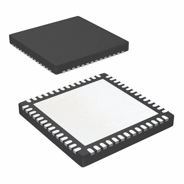
ICGOO电子元器件商城为您提供HMC696LP4E由Hittite设计生产,在icgoo商城现货销售,并且可以通过原厂、代理商等渠道进行代购。 HMC696LP4E价格参考。HittiteHMC696LP4E封装/规格:RF 调制器, RF Modulator IC 20MHz ~ 2.7GHz 24-VFQFN Exposed Pad。您可以下载HMC696LP4E参考资料、Datasheet数据手册功能说明书,资料中有HMC696LP4E 详细功能的应用电路图电压和使用方法及教程。
Analog Devices Inc.的HMC696LP4E是一款RF调制器,主要用于无线通信系统中的射频信号处理。该器件具有高性能、低功耗和小尺寸的特点,适用于多种应用场景。

1. 无线基础设施:HMC696LP4E广泛应用于基站、中继站和其他无线通信基础设施中。它可以在这些设备中实现高效的射频信号调制,确保数据传输的稳定性和可靠性。其高线性度和低相位噪声特性使得它特别适合用于多载波和宽带通信系统。

2. 卫星通信:在卫星通信领域,HMC696LP4E可以用于地面站和卫星之间的信号调制。其宽频带支持和高动态范围使其能够处理复杂的信号调制格式,如QPSK、QAM等,确保高质量的通信链路。

3. 雷达系统:HMC696LP4E在雷达系统中也有广泛应用,特别是在相控阵雷达和脉冲雷达中。它可以用于发射机部分,对射频信号进行精确调制,提高雷达系统的探测精度和分辨率。

4. 测试与测量设备:在测试与测量领域,HMC696LP4E可以集成到信号发生器、频谱分析仪等设备中。它提供了高精度的信号调制功能,帮助工程师进行各种射频性能测试和分析。

5. 军事通信:HMC696LP4E还适用于军事通信系统,如战术电台和安全通信设备。其优异的抗干扰能力和可靠性使得它能够在复杂电磁环境中保持稳定的通信质量。

总之,HMC696LP4E凭借其卓越的性能和灵活性,成为多个领域的理想选择,尤其是在需要高效、可靠射频信号调制的应用场景中。
| 参数 | 数值 |
| 产品目录 | |
| 描述 | IC RFIC I/Q MODULATOR QUAD 24QFN |
| 产品分类 | |
| LO频率 | 20MHz ~ 2.7GHz |
| 品牌 | Hittite Microwave Corporation |
| 数据手册 | |
| 产品图片 |
|
| P1dB | 7dBm |
| 产品型号 | HMC696LP4E |
| RF频率 | 20MHz ~ 2.7GHz |
| rohs | 无铅 / 符合限制有害物质指令(RoHS)规范要求 |
| 产品系列 | - |
| 其它名称 | 1127-1532 |
| 功能 | 调制器 |
| 包装 | 剪切带 (CT) |
| 封装/外壳 | 24-VQFN 裸露焊盘 |
| 本底噪声 | -162dBm/Hz |
| 标准包装 | 1 |
| 测试频率 | - |
| 特色产品 | http://www.digikey.cn/product-highlights/zh/direct-iq-modulators/52283 |
| 电压-电源 | 4.5 V ~ 5.5 V |
| 电流-电源 | 160mA |
| 输出功率 | -1dBm |


- 商务部:美国ITC正式对集成电路等产品启动337调查
- 曝三星4nm工艺存在良率问题 高通将骁龙8 Gen1或转产台积电
- 太阳诱电将投资9.5亿元在常州建新厂生产MLCC 预计2023年完工
- 英特尔发布欧洲新工厂建设计划 深化IDM 2.0 战略
- 台积电先进制程称霸业界 有大客户加持明年业绩稳了
- 达到5530亿美元!SIA预计今年全球半导体销售额将创下新高
- 英特尔拟将自动驾驶子公司Mobileye上市 估值或超500亿美元
- 三星加码芯片和SET,合并消费电子和移动部门,撤换高东真等 CEO
- 三星电子宣布重大人事变动 还合并消费电子和移动部门
- 海关总署:前11个月进口集成电路产品价值2.52万亿元 增长14.8%


PDF Datasheet 数据手册内容提取
HMC696LP4E v04.01213 SiGe WIDEBAND DIRECT QUADRATURE MODULATOR, 20 - 2700 MHz Typical Applications Features The HMC696LP4E is Ideal for: Very Low Noise Floor, -162 dBm/Hz • GMSK, QPSK, QAM, SSB Modulators Excellent Carrier & Sideband Suppression • Cellular/3G and WiMAX/4G Very High Linearity, +23.7 dBm OIP3 E • Software Defined Radio High Output Power, +8.5 dBm Output P1dB • Multi-Band Transmitters High Modulation Accuracy • Test Equipment 24 Lead 4x4 mm QFN Package: 16 mm2 T T M Functional Diagram General DeEscription S The HMC696LP4E is a low noise, high linearity Direct - Quadrature Modulator RFIC which is ideal for digital E modLulation applications from 0.02 to 2.7 GHz inc- R luding software defined radio and multi-band tran- U smitters. Housed in a compact 4x4 mm (LP4) SMT T O QFN package, the RFIC requires minimal external A components & provides a low cost alternative to more R complicated double upconversion architectures. The D RF output port is single-ended and matched to 50 A S Ohms with no external components. The LO requires U 0 to +10 dBm and can be driven in either differential Q or single-ended mode. This device is optimized for a T +5V supply, and offers improved carrier feedthrough B C and sideband suppression characteristics. For higher E frequency applications, the HMC697LP4E Direct R Modulator covers 450 - 4000 MHz. I D O - S R O Electrical Specifications, See Test Conditions on following page herein. T A Parameter Typ. Typ. Typ. Typ. Typ. Typ. Typ. Units L Frequency Range, RF 20 - 40 40 - 100 100 - 450 450 - 960 960 - 1700 1700 - 2200 2200 - 2700 MHz U Output P1dB 7 8 8 8 7 6 5 dBm D Output Noise Floor -160 -162 -163 -162 -162 -161 dBm/Hz O Output IP3 21 24 24 23 21 19 17 dBm M Output Power 0 1 1 0 -1 -2 -3 dBm Carrier Feedthrough (uncalibrated) -42 -42 -42 -42 -43 -45 -42 dBm Sideband Suppression -29 -40 -54 -42 -43 -42 -30 dBc (uncalibrated) LO Port Return Loss 9 12 15 15 11 7 5 dB RF Port Return Loss 29 28 29 31 30 24 20 dB InFfoormra tpiorni cfuern,is hdeed lbivy eArnyal oag nDdev itcoes pisl abcelieev eodr dto ebres a: cHcuirtatteit ean dM reicliarbolew. Haovweev eCr, onor poFroart ipornic,e 2, dEelliivzearby,e atnhd D tor ivpela,c eC horedlemrss: fAonradlo, gM DAe v0ic1e8s2, 4Inc., responsibility is assumed by Analog Devices for its use, nor for any infringements of patents or other One Technology Way, P.O. Box 9106, Norwood, MA 02062-9106 1 rliicgehntss eo fi sth girrda nptaerdti ebsy t himatp mlicPaayht ioroens nuolret of:rto hm9er 7wits8is ue-s 2eu.n5 dS0epre- ca3infi3yc ap4tiao3tne sn ts ou rb Fjpeaactte xtno:t cr9higa7hnt8gs e-o 2wf Ai5thn0oaulo-t g3n oD3tiec7vei3.c eN s o. OPrhdoneer: O78n1--3li2n9e- 4a7t0 0w (cid:127)w Owrd.ehri totnitlein.ec aot mwww.analog.com Trademarks and registered trademarks aArep thpe lpircopaetrityo onf thSeiur rpesppeoctrivte: oPwhneorsn.e: 978-250-33A4p3p l icoart i oanp Spusp@pohrti:t Ptihteon.ceo: 1m-800-ANALOG-D
HMC696LP4E v04.1213 SiGe WIDEBAND DIRECT QUADRATURE MODULATOR, 20 - 2700 MHz Electrical Specifications, (continued) Parameter Conditions Min. Typ. Max. Units RF Output RF Frequency Range 20 2700 MHz RF Return Loss 27 dB E LO Input LO Frequency Range 20 2700 MHz LO Input Power 0 10 dBm LO Port Return Loss T10 dB Baseband Input Port Baseband Input DC Voltage (Vbbdc) 1.5 1.7 V T Baseband Input DC Bias Current (Ibbdc) Single-ended. E 60 µA M Single-ended Baseband Input Capacitance De-embed to the lead of the device. 4.5 pF S DC Power Requirements See Test Conditions Below Supply Voltage (Vcc1, Vcc2) 4.5 5 5.5 V - Supply Current (Icc1 + Icc2) L 140 160 180 mA E R Test Conditions: Unless Otherwise Specified, the Following Test Conditions Were Used U T O Parameter Condition A Temperature +25 °C R Baseband Input Frequency 200 kHz D Baseband Input DC Voltage (Vbbdc) +1.5V A Baseband Input AC Voltage (PSeak to Peak Differential, I and Q) +1.4V U Baseband Input AC Voltage for OIP3 Measurement (Peak to Peak Differential, I and Q) 700 mV per tone @ 150 & 250 kHz Q Frequency Offset for Output Noise Measurements 30 MHz T Supply (Vcc1, Vcc2) +5V B C LO Input Power 0 dBm E LO Input Mode Single-Ended through LOP R Mounting Configuration Refer to HMC696LP4E Application Schematic Herein I Sideband & Carrier FeedthOrough Uncalibrated D - S R Calibrated vs. Uncalibrated Test Results O During the Uncalibrated Sideband and Carrier Suppression tests, care is taken to ensure that the I/Q signal paths from T A the Vector Signal Generator (VSG) to the Device Under Test (DUT) are equal. The “Uncalibrated, +25 °C” Sideband and Carrier Suppression plots were measured at room temperature, while the “Uncalibrated, over Temperature” L U Sideband and Carrier Suppression plots represent the worst case uncalibrated suppression levels measured at T= D -40 °C, +25 °C, and +85 °C. O The “Calibrated, + 25 °C” Sideband Suppression data was plotted after a manual adjustment of the I/Q amplitude M balance and I/Q phase offset (skew) at +25 °C, and at each LO input power level. The +25 °C adjustment settings were held constant during tests over temperature. The “Calibrated, over Temperature” plots represent the worst case calibrated Sideband Suppression levels at T= -40 °C, +25 °C, and +85 °C. The “Calibrated, +25 °C” Carrier Suppression data was plotted after a manual adjustment of the Ip/In & Qp/Qn DC offsets at +25 °C, and at each LO input power level. The +25 °C adjustment settings were held constant during tests over temperature. The “Calibrated, over Temperature” plots represent the worst case Carrier Suppression levels measured at T= -40 °C, +25 °C, and +85 °C. InFfoormra tpiorni cfuern,is hdeed lbivy eArnyal oag nDdev itcoes pisl abcelieev eodr dto ebres a: cHcuirtatteit ean dM reicliarbolew. Haovweev eCr, onor poFroart ipornic,e 2, dEelliivzearby,e atnhd D tor ivpela,c eC horedlemrss: fAonradlo, gM DAe v0ic1e8s2, 4Inc., responsibility is assumed by Analog Devices for its use, nor for any infringements of patents or other One Technology Way, P.O. Box 9106, Norwood, MA 02062-9106 rights of third parties that mPayh roesnulet f:ro m9 7its8 u-s2e.5 S0pe-c3ifi3ca4tio3n s s u bFjeact xto: c9ha7n8ge- 2wi5th0ou-t 3no3tic7e3. N o OPrhdoneer: O78n1--3li2n9e- 4a7t0 0w (cid:127)w Owrd.ehri totnitlein.ec aot mwww.analog.com 2 license is granted by implication or otherwise under any patent or patent rights of Analog Devices. Trademarks and registered trademarks aArep thpe lpircopaetrityo onf thSeiur rpesppeoctrivte: oPwhneorsn.e: 978-250-33A4p3p l icoart i oanp Spusp@pohrti:t Ptihteon.ceo: 1m-800-ANALOG-D
HMC696LP4E v04.1213 SiGe WIDEBAND DIRECT QUADRATURE MODULATOR, 20 - 2700 MHz Output IP3, P1dB & Noise Floor Wideband Performance vs. Frequency @ 30 MHz Offset vs. Frequency 10 m) 30 -120O B U d T Bm) 5 ++-428055CCC T IP3 ( 20 OUTPUT IP3 -130PUT N WER (d OUTPU 10 OUTPUT P1dB E -140OISE F PUT PO 0 dBm) & 0 ++-428055CCC -150LOOR @ OUT -5 1dB (-10 T -16030 M MT -1010 100 1000 10000 OUTPUT P--320010 E100 SET1-0U0P0 NONISOEI SFEL OFOLOROR100--01108700Hz (dBm/Hz) S FREQUENCY (MHz) FREQUENCY (MHz) - E Uncalibrated Carrier Feedthrough [1] CalLibrated Carrier Feedthrough [1] R vs. Frequency Over Temperature vs. Frequency Over Temperature U 0 0 T A Bm)-10 +25C O Bm)-10 R H (d-20 +-4805CC H (d-20 +25C G G +85C D OU-30 OU-30 -40C A HR-40 HR-40 T T D S D U E-50 E-50 E E F F Q R -60 R -60 E E T ARRI-70 ARRI-70 C-80 B C-80 C E -90 -90 10 100 1000 10000 10 100 1000 10000 R FREQUENCY (MHz) FREQUENCY (MHz) I D O - S Sideband Suppression vs. Frequency Return Loss vs. Frequency R 0 0 O T dBc)-10 +25C -5 A ON (-20 +-4805CC B)-10 L SSI S (d U RE-30 OS-15 P L OD D SUP-40 TURN -20 LROF N E A-50 R-25 M EB D SI-60 -30 -70 -35 10 100 1000 10000 10 100 1000 10000 FREQUENCY (MHz) FREQUENCY (MHz) [1] See note titled “Calibrated vs. Uncalibrated test results” herein. InFfoormra tpiorni cfuern,is hdeed lbivy eArnyal oag nDdev itcoes pisl abcelieev eodr dto ebres a: cHcuirtatteit ean dM reicliarbolew. Haovweev eCr, onor poFroart ipornic,e 2, dEelliivzearby,e atnhd D tor ivpela,c eC horedlemrss: fAonradlo, gM DAe v0ic1e8s2, 4Inc., responsibility is assumed by Analog Devices for its use, nor for any infringements of patents or other One Technology Way, P.O. Box 9106, Norwood, MA 02062-9106 3 rliicgehntss eo fi sth girrda nptaerdti ebsy t himatp mlicPaayht ioroens nuolret of:rto hm9er 7wits8is ue-s 2eu.n5 dS0epre- ca3infi3yc ap4tiao3tne sn ts ou rb Fjpeaactte xtno:t cr9higa7hnt8gs e-o 2wf Ai5thn0oaulo-t g3n oD3tiec7vei3.c eN s o. OPrhdoneer: O78n1--3li2n9e- 4a7t0 0w (cid:127)w Owrd.ehri totnitlein.ec aot mwww.analog.com Trademarks and registered trademarks aArep thpe lpircopaetrityo onf thSeiur rpesppeoctrivte: oPwhneorsn.e: 978-250-33A4p3p l icoart i oanp Spusp@pohrti:t Ptihteon.ceo: 1m-800-ANALOG-D
HMC696LP4E v04.1213 SiGe WIDEBAND DIRECT QUADRATURE MODULATOR, 20 - 2700 MHz Wideband Performance Output IP3, P1dB & Noise Floor @ 30 MHz vs. Frequency Over LO Power Offset vs. Frequency Over LO Power 10 0 m) 30 -120O B U 0 dBm d T OUTPUT POWER (dBm) -505 OUTPUT POWE+R +106 ddBBmm ---431505SIDEBAND SUPPRESSION 1dB (dBm) & OUTPUT IP3 (-1120000 OUTPUT IP3 OUTTPUT+ + 1P 0061 ddddBBBBmmm E ----111165430000PUT NOISE FLOOR @30 M -1010 100 SID1E0B0A0ND SUPPRESSIO1N000-600 (dBc) OUTPUT P--320010 E100 SET1-0U0P0 NONISOEI SFEL OFOLOROR100--01108700Hz (dBm/Hz) MT FREQUENCY (MHz) FREQUENCY (MHz) S - Uncalibrated Carrier Feedthrough [1] CalLibrated Carrier Feedthrough [1] E vs. Frequency Over LO Power vs. Frequency Over LO Power R U 0 0 T Bm)-10 0 dBm O Bm)-10 A H (d-20 + +106 ddBBmm H (d-20 0 dBm R G G +6 dBm OU-30 OU-30 +10 dBm D HR-40 HR-40 A T T D S D E-50 E-50 U E E F F R -60 R -60 Q E E ARRI-70 ARRI-70 T C-80 B C-80 C -90 -90 E 10 100 1000 10000 10 100 1000 10000 FREQUENCY (MHz) FREQUENCY (MHz) R I O D Output IP3, P1dB & Noise Floor Wideband Performance @ 30 MHz Offset vs. Frequency - vs. Frequency Over Supply Voltage Over Supply Voltage S R 10 0 m) 30 -120O O B U OUTPUT POWER (dBm) -505 OUTPUT POWER455...505VVV ---431505SIDEBAND SUPPRESSION 1dB (dBm) & OUTPUT IP3 (d-1120000 OUTPUT IP3 OUTPUT455 P...5051 dVVVB ----111165430000TPUT NOISE FLOOR @30 M MODULAT -1010 100 SID1E0B0A0ND SUPPRESSIO1N000-600 (dBc) OUTPUT P--3200 SET-UP NONISOEIS FEL OFLOOROR --118700Hz (dBm/H 10 100 1000 10000 z) FREQUENCY (MHz) FREQUENCY (MHz) [1] See note titled “Calibrated vs. Uncalibrated test results” herein. InFfoormra tpiorni cfuern,is hdeed lbivy eArnyal oag nDdev itcoes pisl abcelieev eodr dto ebres a: cHcuirtatteit ean dM reicliarbolew. Haovweev eCr, onor poFroart ipornic,e 2, dEelliivzearby,e atnhd D tor ivpela,c eC horedlemrss: fAonradlo, gM DAe v0ic1e8s2, 4Inc., responsibility is assumed by Analog Devices for its use, nor for any infringements of patents or other One Technology Way, P.O. Box 9106, Norwood, MA 02062-9106 rights of third parties that mPayh roesnulet f:ro m9 7its8 u-s2e.5 S0pe-c3ifi3ca4tio3n s s u bFjeact xto: c9ha7n8ge- 2wi5th0ou-t 3no3tic7e3. N o OPrhdoneer: O78n1--3li2n9e- 4a7t0 0w (cid:127)w Owrd.ehri totnitlein.ec aot mwww.analog.com 4 license is granted by implication or otherwise under any patent or patent rights of Analog Devices. Trademarks and registered trademarks aArep thpe lpircopaetrityo onf thSeiur rpesppeoctrivte: oPwhneorsn.e: 978-250-33A4p3p l icoart i oanp Spusp@pohrti:t Ptihteon.ceo: 1m-800-ANALOG-D
HMC696LP4E v04.1213 SiGe WIDEBAND DIRECT QUADRATURE MODULATOR, 20 - 2700 MHz Output IP3, P1dB & Noise Floor @ 30 MHz Output Noise @ 30 MHz Offset vs. Offset vs. Frequency Over Input RF Output Power Baseband DC Voltage -130 OUTPUT IP3 (dBm) 123000 OUTPUT IP3 OUTPUT P1dB ---111432000OUTPUT NOISE F 30 MHz (dBm/Hz)---111443505 LO Freque 1 n993c300y MMHHzz E dBm) & 0 111...567 VVV -150LOOR @ OISE @ --115550 T 1dB (-10 -16030 M UT N-160 MT OUTPUT P--3200 SET-UP NONISOEI SFEL OFOLOROR --118700Hz (dBm/H OUTP--117605-30 -25 E-20 -15 -10 -5 0 5 10 S 10 100 1000 10000 z) RF OUTPUT POWER (dBm) FREQUENCY (MHz) - E L Supply Current vs. R U Input Baseband DC Voltage Absolute Maximum Ratings T 180 O Vcc1, Vcc2 +6V A +25C LO Input Power +18 dBm R 175 +85C D T (mA)170 -40C B(Raesfeebreanncde I ntop uGt NVDol)tage (AC + DC) 0V to +2.8V A REN S Junction Temperature 150 °C QU Y CUR165 C(Doenrtainteu o3u0s m PWdi/s°sC ( aTb =o v8e5 °8C5)°C) 1.8 Watts PL160 CT SUP155 B T(juhnecrmtioanl Rtoe gsirsotuanndc ep a(Rdtdh)le) 34 °C/W Storage Temperature -65 to +150 °C E R 1501.5 1.6 1.7 Operating Temperature -40 to +85 °C I INPUT BASEBAND DC VOLTAGE (V) D O - S ELECTROSTATIC SENSITIVE DEVICE R OBSERVE HANDLING PRECAUTIONS O T A L U D O M InFfoormra tpiorni cfuern,is hdeed lbivy eArnyal oag nDdev itcoes pisl abcelieev eodr dto ebres a: cHcuirtatteit ean dM reicliarbolew. Haovweev eCr, onor poFroart ipornic,e 2, dEelliivzearby,e atnhd D tor ivpela,c eC horedlemrss: fAonradlo, gM DAe v0ic1e8s2, 4Inc., responsibility is assumed by Analog Devices for its use, nor for any infringements of patents or other One Technology Way, P.O. Box 9106, Norwood, MA 02062-9106 5 rliicgehntss eo fi sth girrda nptaerdti ebsy t himatp mlicPaayht ioroens nuolret of:rto hm9er 7wits8is ue-s 2eu.n5 dS0epre- ca3infi3yc ap4tiao3tne sn ts ou rb Fjpeaactte xtno:t cr9higa7hnt8gs e-o 2wf Ai5thn0oaulo-t g3n oD3tiec7vei3.c eN s o. OPrhdoneer: O78n1--3li2n9e- 4a7t0 0w (cid:127)w Owrd.ehri totnitlein.ec aot mwww.analog.com Trademarks and registered trademarks aArep thpe lpircopaetrityo onf thSeiur rpesppeoctrivte: oPwhneorsn.e: 978-250-33A4p3p l icoart i oanp Spusp@pohrti:t Ptihteon.ceo: 1m-800-ANALOG-D
HMC696LP4E v04.1213 SiGe WIDEBAND DIRECT QUADRATURE MODULATOR, 20 - 2700 MHz Outline Drawing E T T E M S - L E R U T O A R Package Information D Part Number Package Body Material Lead Finish MSL Rating Package Marking [1] A S HMC696LP4E RoHS-compliant Low Stress Injection Molded Plastic 100% matte Sn MSL1 [2] H696 U XXXX Q [1] 4-Digit lot number XXXX [2] Max peak reflow temperature of 260 °C T B C E R I O D - S R O T A L U D O M InFfoormra tpiorni cfuern,is hdeed lbivy eArnyal oag nDdev itcoes pisl abcelieev eodr dto ebres a: cHcuirtatteit ean dM reicliarbolew. Haovweev eCr, onor poFroart ipornic,e 2, dEelliivzearby,e atnhd D tor ivpela,c eC horedlemrss: fAonradlo, gM DAe v0ic1e8s2, 4Inc., responsibility is assumed by Analog Devices for its use, nor for any infringements of patents or other One Technology Way, P.O. Box 9106, Norwood, MA 02062-9106 rights of third parties that mPayh roesnulet f:ro m9 7its8 u-s2e.5 S0pe-c3ifi3ca4tio3n s s u bFjeact xto: c9ha7n8ge- 2wi5th0ou-t 3no3tic7e3. N o OPrhdoneer: O78n1--3li2n9e- 4a7t0 0w (cid:127)w Owrd.ehri totnitlein.ec aot mwww.analog.com 6 license is granted by implication or otherwise under any patent or patent rights of Analog Devices. Trademarks and registered trademarks aArep thpe lpircopaetrityo onf thSeiur rpesppeoctrivte: oPwhneorsn.e: 978-250-33A4p3p l icoart i oanp Spusp@pohrti:t Ptihteon.ceo: 1m-800-ANALOG-D
HMC696LP4E v04.1213 SiGe WIDEBAND DIRECT QUADRATURE MODULATOR, 20 - 2700 MHz Pin Descriptions Pin Number Function Description Interface Schematic 1, 6, 7, 13, 15 N/C Not connected. 2, 5, 8, 11, These pins and the ground paddle should be 12, 14, 17, 19, GND connected to a high quality RF/DC ground. E 20, 23 LO inputs. Need DC decoupling capacitors. T 3, 4 LOP, LON The ports could be driven single ended or differentially. T M E S Q channel differential baseband input. These high - impedance ports should be biased around 1.5V DC. E 9, 10 QN, QP Nominal recommended baseband inpuLt is around R 700 mV pp differential. U T O A R D DC coupled and matched to 50 Ohms, A 16 RFOUT output requires blocking capacitor. S U Q T B C E Supply voltage for the mixer and 18 Vcc1 R output stages 74mA @ +5V. I D O - S I channel differential baseband input. R 21, 22 IP, IN These high impedance ports should be at the same bias voltage (VbbDC) as QN & QP. O T A L U 24 Vcc2 Supply voltage for the LO stage 85mA @ +5V. D O M InFfoormra tpiorni cfuern,is hdeed lbivy eArnyal oag nDdev itcoes pisl abcelieev eodr dto ebres a: cHcuirtatteit ean dM reicliarbolew. Haovweev eCr, onor poFroart ipornic,e 2, dEelliivzearby,e atnhd D tor ivpela,c eC horedlemrss: fAonradlo, gM DAe v0ic1e8s2, 4Inc., responsibility is assumed by Analog Devices for its use, nor for any infringements of patents or other One Technology Way, P.O. Box 9106, Norwood, MA 02062-9106 7 rliicgehntss eo fi sth girrda nptaerdti ebsy t himatp mlicPaayht ioroens nuolret of:rto hm9er 7wits8is ue-s 2eu.n5 dS0epre- ca3infi3yc ap4tiao3tne sn ts ou rb Fjpeaactte xtno:t cr9higa7hnt8gs e-o 2wf Ai5thn0oaulo-t g3n oD3tiec7vei3.c eN s o. OPrhdoneer: O78n1--3li2n9e- 4a7t0 0w (cid:127)w Owrd.ehri totnitlein.ec aot mwww.analog.com Trademarks and registered trademarks aArep thpe lpircopaetrityo onf thSeiur rpesppeoctrivte: oPwhneorsn.e: 978-250-33A4p3p l icoart i oanp Spusp@pohrti:t Ptihteon.ceo: 1m-800-ANALOG-D
HMC696LP4E v04.1213 SiGe WIDEBAND DIRECT QUADRATURE MODULATOR, 20 - 2700 MHz Evaluation PCB E T T E M S - L E R U T O A R D A S U Q T B C E R I O D - List of Materials for Evaluation PCB 121963 [1] S R The circuit board used in the final application should Item Description O use RF circuit design techniques. Signal lines J1 - J7 PCB Mount SMA Connector T should have 50 ohm impedance while the package J8, J9 DC Molex Connector A ground leads and exposed paddle should be con- C1 - C3 0.1 µF Chip Capacitor, 0402 Pkg. L nected directly to the ground plane similar to that U C4, C5 1000 pF Chip Capacitor, 0402 Pkg. shown. A sufficient number of via holes should be D C6, C7 4.7 µF, Case A, Tantalum used to connect the top and bottom ground planes. O R1 14 Ohm Resistor, 0402 Pkg. The evaluation circuit board shown is available from M R2 0 Ohm Resistor, 0402 Pkg. Hittite upon request. U1 HMC696LP4E Modulator PCB [2] 121961 Eval Board [1] Reference this number when ordering complete evaluation PCB [2] Circuit Board Material: Rogers 4350 InFfoormra tpiorni cfuern,is hdeed lbivy eArnyal oag nDdev itcoes pisl abcelieev eodr dto ebres a: cHcuirtatteit ean dM reicliarbolew. Haovweev eCr, onor poFroart ipornic,e 2, dEelliivzearby,e atnhd D tor ivpela,c eC horedlemrss: fAonradlo, gM DAe v0ic1e8s2, 4Inc., responsibility is assumed by Analog Devices for its use, nor for any infringements of patents or other One Technology Way, P.O. Box 9106, Norwood, MA 02062-9106 rights of third parties that mPayh roesnulet f:ro m9 7its8 u-s2e.5 S0pe-c3ifi3ca4tio3n s s u bFjeact xto: c9ha7n8ge- 2wi5th0ou-t 3no3tic7e3. N o OPrhdoneer: O78n1--3li2n9e- 4a7t0 0w (cid:127)w Owrd.ehri totnitlein.ec aot mwww.analog.com 8 license is granted by implication or otherwise under any patent or patent rights of Analog Devices. Trademarks and registered trademarks aArep thpe lpircopaetrityo onf thSeiur rpesppeoctrivte: oPwhneorsn.e: 978-250-33A4p3p l icoart i oanp Spusp@pohrti:t Ptihteon.ceo: 1m-800-ANALOG-D
HMC696LP4E v04.1213 SiGe WIDEBAND DIRECT QUADRATURE MODULATOR, 20 - 2700 MHz Application & Evaluation PCB Schematic E T T M E S - E L R U T O A R D A S U Q T B C E Characterization Set-up R I D O - S R O T A L U D O M InFfoormra tpiorni cfuern,is hdeed lbivy eArnyal oag nDdev itcoes pisl abcelieev eodr dto ebres a: cHcuirtatteit ean dM reicliarbolew. Haovweev eCr, onor poFroart ipornic,e 2, dEelliivzearby,e atnhd D tor ivpela,c eC horedlemrss: fAonradlo, gM DAe v0ic1e8s2, 4Inc., responsibility is assumed by Analog Devices for its use, nor for any infringements of patents or other One Technology Way, P.O. Box 9106, Norwood, MA 02062-9106 9 rliicgehntss eo fi sth girrda nptaerdti ebsy t himatp mlicPaayht ioroens nuolret of:rto hm9er 7wits8is ue-s 2eu.n5 dS0epre- ca3infi3yc ap4tiao3tne sn ts ou rb Fjpeaactte xtno:t cr9higa7hnt8gs e-o 2wf Ai5thn0oaulo-t g3n oD3tiec7vei3.c eN s o. OPrhdoneer: O78n1--3li2n9e- 4a7t0 0w (cid:127)w Owrd.ehri totnitlein.ec aot mwww.analog.com Trademarks and registered trademarks aArep thpe lpircopaetrityo onf thSeiur rpesppeoctrivte: oPwhneorsn.e: 978-250-33A4p3p l icoart i oanp Spusp@pohrti:t Ptihteon.ceo: 1m-800-ANALOG-D
HMC696LP4E v04.1213 SiGe WIDEBAND DIRECT QUADRATURE MODULATOR, 20 - 2700 MHz Notes: E T T E M S - L E R U T O A R D A S U Q T B C E R I O D - S R O T A L U D O M InFfoormra tpiorni cfuern,is hdeed lbivy eArnyal oag nDdev itcoes pisl abcelieev eodr dto ebres a: cHcuirtatteit ean dM reicliarbolew. Haovweev eCr, onor poFroart ipornic,e 2, dEelliivzearby,e atnhd D tor ivpela,c eC horedlemrss: fAonradlo, gM DAe v0ic1e8s2, 4Inc., responsibility is assumed by Analog Devices for its use, nor for any infringements of patents or other One Technology Way, P.O. Box 9106, Norwood, MA 02062-9106 rights of third parties that mPayh roesnulet f:ro m9 7its8 u-s2e.5 S0pe-c3ifi3ca4tio3n s s u bFjeact xto: c9ha7n8ge- 2wi5th0ou-t 3no3tic7e3. N o OPrhdoneer: O78n1--3li2n9e- 4a7t0 0w (cid:127)w Owrd.ehri totnitlein.ec aot mwww.analog.com 10 license is granted by implication or otherwise under any patent or patent rights of Analog Devices. Trademarks and registered trademarks aArep thpe lpircopaetrityo onf thSeiur rpesppeoctrivte: oPwhneorsn.e: 978-250-33A4p3p l icoart i oanp Spusp@pohrti:t Ptihteon.ceo: 1m-800-ANALOG-D