ICGOO在线商城 > 射频/IF 和 RFID > RF 开关 > HMC646LP2E

 Datasheet下载
- 型号: HMC646LP2E
- 制造商: Hittite
- 库位|库存: xxxx|xxxx
- 要求:
| 数量阶梯 | 香港交货 | 国内含税 |
| +xxxx | $xxxx | ¥xxxx |
查看当月历史价格
查看今年历史价格
HMC646LP2E产品简介:
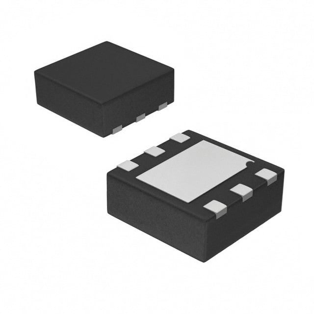
ICGOO电子元器件商城为您提供HMC646LP2E由Hittite设计生产,在icgoo商城现货销售,并且可以通过原厂、代理商等渠道进行代购。 HMC646LP2E价格参考¥62.59-¥62.59。HittiteHMC646LP2E封装/规格:RF 开关, 射频开关 IC 手机,TD-SCDMA SPDT 2.1GHz 50 欧姆 6-DFN(2x2)。您可以下载HMC646LP2E参考资料、Datasheet数据手册功能说明书,资料中有HMC646LP2E 详细功能的应用电路图电压和使用方法及教程。
| 参数 | 数值 |
| 产品目录 | |
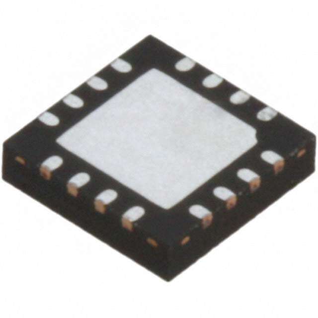
| 描述 | IC SWITCH SPDT FAILSAFE 6-DFN |
| 产品分类 | |
| IIP3 | 34dBm (标准) |
| 品牌 | Hittite Microwave Corporation |
| 数据手册 | |
| 产品图片 |
|
| P1dB | - |
| 产品型号 | HMC646LP2E |
| RF类型 | 手机,TD-SCDMA |
| rohs | 无铅 / 符合限制有害物质指令(RoHS)规范要求 |
| 产品系列 | - |
| 供应商器件封装 | 6-DFN(2x2) |
| 其它名称 | 1127-1503 |
| 包装 | 剪切带 (CT) |
| 封装/外壳 | 6-TDFN 裸露焊盘 |
| 工作温度 | -40°C ~ 85°C |
| 拓扑 | 反射 |
| 插损@频率 | 1.3dB @ 2.025GHz |
| 标准包装 | 1 |
| 特性 | - |
| 电压-电源 | 3 V ~ 8 V |
| 电路 | SPDT |
| 阻抗 | 50 欧姆 |
| 隔离@频率 | 32dB @ 2.025GHz (标准) |
| 频率 -上 | 2.1GHz |
| 频率 -下 | 100MHz |


- 商务部:美国ITC正式对集成电路等产品启动337调查
- 曝三星4nm工艺存在良率问题 高通将骁龙8 Gen1或转产台积电
- 太阳诱电将投资9.5亿元在常州建新厂生产MLCC 预计2023年完工
- 英特尔发布欧洲新工厂建设计划 深化IDM 2.0 战略
- 台积电先进制程称霸业界 有大客户加持明年业绩稳了
- 达到5530亿美元!SIA预计今年全球半导体销售额将创下新高
- 英特尔拟将自动驾驶子公司Mobileye上市 估值或超500亿美元
- 三星加码芯片和SET,合并消费电子和移动部门,撤换高东真等 CEO
- 三星电子宣布重大人事变动 还合并消费电子和移动部门
- 海关总署:前11个月进口集成电路产品价值2.52万亿元 增长14.8%


PDF Datasheet 数据手册内容提取
HMC646LP2 646LP2E / v02.1009 GaAs MMIC 40W FAILSAFE SWITCH, 0.1 - 2.1 GHz Typical Applications Features The HMC646LP2(E) is ideal for: High Input P0.1dB: +46 dBm Tx • LNA Protection & T/R Switching Low Insertion Loss: 0.4 dB • TD-SCDMA / 3G Infrastructure High IIP3: +74 dBm • Satellite Subscriber Terminals Single Positive Control: 0/+3V to 0/+8V • Private Mobile Radio & Public Safety Handsets Failsafe operation; Tx ‘On’ when unpowered • Automotive Telematics 2x2mm DFN SMT Package Functional Diagram General Description The HMC646LP2(E) is an SPDT switch in a leadless DFN surface mount plastic package for use in trans- 11 mit / receive and LNA protection applications which require very low distortion and high power handling of up to 40 watts with less than 10% duty cycle. This robust switch can control signals from 100 - 2100 T M MHz* and is ideal for TD-SCDMA / 3G repeaters, PMR, automotive telematics, and satellite subscriber S terminal applications. The design provides excep- - tional P0.1dB of +46 dBm and +74 dBm IIP3 on the T Transmit (Tx) port. The failsafe topology provides a D low loss path from Tx to RFC, when no DC power is P S available. - S Electrical Specifi cations, T = +25°C, Vdd= 5V, Vctl = 0/+5 Vdc, 50 Ohm System* E A H Parameter Min. Typ. Max. Min. Typ. Max. Min. Typ. Max Units C Frequency Range 869 - 960 1525 - 1661 2010 - 2025 MHz T Tx - RFC 0.3 0.6 0.6 0.9 0.7 1.0 dB I Insertion Loss W RFC - Rx 0.4 0.7 0.8 1.1 1.3 1.7 dB Tx - RFC 20 27 15 22 12 17 dB S Isolation RFC - Rx 28 38 20 30 25 32 dB Tx - RFC 17 27 25 dB Return Loss RFC - Rx 25 20 12 dB Input Power for 0.1 dB Tx - RFC 44 46 46 dBm Compression RFC - Rx 20 20 20 dBm Input Third Order Tx - RFC 71 74 74 dBm Intercept (Two-tone input RFC - Rx 41 42 34 dBm power = +17 dBm each tone) Switching Characteristics tRISE, tFALL (10/90% RF) 100 100 100 ns tON, (50% CTL to 90% RF) 320 320 320 ns tOFF (50% CTL to 10% RF) 320 320 320 ns * Specifi cations and data refl ect HMC646LP2(E) measured using the respective application circuits for each designated frequency band found herein Information furnishFedo rb yp Arniacloeg ,D deveicleisv eis rbye,li eavend dto tboe apclcaurcatee aondr dreeliarbsle,. pHoleweavesr,e n oc onFtoar cptr icHei,t tdieteliv eMryi,c arnodw toa vpela cCeo orrpdeorrsa: tAionanlo:g Devices, Inc., responsibility is assumed by Analog Devices for its use, nor for any infringements of patents or other One Technology Way, P.O. Box 9106, Norwood, MA 02062-9106 11 - 216 rights of third parties th2a0t m Aay lrpeshulat fr oRm oitsa udse,. SCpehceificlamtiosnsf osurbdje,c t Mto cAha n0g1e 8wi2th4ou t Pnohticoe.n Neo : 9P7h8o-n2e:5 708-13-33249-34 7 0F0a (cid:127)x O: r9d7er8 o-n2li5ne0 a-t3 w3w7w3.analog.com license is granted by implication or otherwise under any patent or patent rights of Analog Devices. Trademarks and registered trademarks are the property of their reOspredctiever o Ownners-.line at www.hAitptiptleic.actioomn Support: Phone: 1-800-ANALOG-D
HMC646LP2 / 646LP2E v02.1009 GaAs MMIC 40W FAILSAFE SWITCH, 0.1 - 2.1 GHz Insertion Loss vs. Temperature, Insertion Loss vs. Temperature, Tx with 915 MHz Tuning Rx with 915 MHz Tuning 0 0 -0.25 B) -0.5 B) -0.5 d d SS ( SS (-0.75 O O N L -1 ++2855CC N L -1 O -40C O SERTI SERTI-1.25 ++2855CC N -1.5 N -1.5 -40C I I -1.75 -2 -2 0.8 0.85 0.9 0.95 1 0.8 0.85 0.9 0.95 1 FREQUENCY (GHz) FREQUENCY (GHz) 11 Isolation with 915 MHz Tuning Return Loss with 915 MHz Tuning 0 0 Tx, Input OLATION (dB) ---321000 RRFFCC ttoo RTxX URN LOSS (dB) --2100 TRRxxx,,, OIOnuupttupptuutt - SMT IS RET -30 DT -40 P S -50 -40 0.8 0.85 0.9 0.95 1 0.8 0.85 0.9 0.95 1 - FREQUENCY (GHz) FREQUENCY (GHz) S E H C Input IP3 vs. Voltage with 915 MHz Tuning T 75 I 70 W 65 S 60 Tx m) 55 Rx B d 50 3 ( P 45 I 40 35 30 25 3 4 5 6 7 8 VOLTAGE (V) Information furnishFedo rb yp Arniacloeg ,D deveicleisv eis rbye,li eavend dto tboe apclcaurcatee aondr dreeliarbsle,. pHoleweavesr,e n oc onFtoar cptr icHei,t tdieteliv eMryi,c arnodw toa vpela cCeo orrpdeorrsa: tAionanlo:g Devices, Inc., responsibility is assumed by Analog Devices for its use, nor for any infringements of patents or other One Technology Way, P.O. Box 9106, Norwood, MA 02062-9106 rights of third parties th2a0t m Aay lrpeshulat fr oRm oitsa udse,. SCpehceificlamtiosnsf osurbdje,c t Mto cAha n0g1e 8wi2th4ou t Pnohticoe.n Neo : 9P7h8o-n2e:5 708-13-33249-34 7 0F0a (cid:127)x O: r9d7er8 o-n2li5ne0 a-t3 w3w7w3.analog.com 11 - 217 license is granted by implication or otherwise under any patent or patent rights of Analog Devices. Trademarks and registered trademarks are the property of their reOspredctiever o Ownners-.line at www.hAitptiptleic.actioomn Support: Phone: 1-800-ANALOG-D
HMC646LP2 / 646LP2E v02.1009 GaAs MMIC 40W FAILSAFE SWITCH, 0.1 - 2.1 GHz Insertion Loss vs. Temperature, Insertion Loss vs. Temperature, Tx with 1600 MHz Tuning Rx with 1600 MHz Tuning 0 0 B) -0.5 B) -0.5 d d S ( S ( S S O O L L N -1 N -1 O O TI TI R R E E S +25C S +25C IN -1.5 +-4805CC IN -1.5 +-4805CC -2 -2 1.5 1.55 1.6 1.65 1.7 1.5 1.55 1.6 1.65 1.7 FREQUENCY (GHz) FREQUENCY (GHz) 11 Isolation with 1600 MHz Tuning Return Loss with 1600 MHz Tuning 0 0 Tx, Input - SMT OLATION (dB) ---321000 RRFFCC ttoo TRxX URN LOSS (dB) --2100 TRRxxx,,, OIOnuupttupptuutt DT IS RET -30 -40 P S -50 -40 1.5 1.55 1.6 1.65 1.7 1.5 1.55 1.6 1.65 1.7 - FREQUENCY (GHz) FREQUENCY (GHz) S E H C Input IP3 vs. Voltage with 1600 MHz Tuning T 80 I W 75 70 S 65 60 Bm) 55 RTxx d 3 ( 50 P I 45 40 35 30 25 3 4 5 6 7 8 VOLTAGE (V) Information furnishFedo rb yp Arniacloeg ,D deveicleisv eis rbye,li eavend dto tboe apclcaurcatee aondr dreeliarbsle,. pHoleweavesr,e n oc onFtoar cptr icHei,t tdieteliv eMryi,c arnodw toa vpela cCeo orrpdeorrsa: tAionanlo:g Devices, Inc., responsibility is assumed by Analog Devices for its use, nor for any infringements of patents or other One Technology Way, P.O. Box 9106, Norwood, MA 02062-9106 11 - 218 rights of third parties th2a0t m Aay lrpeshulat fr oRm oitsa udse,. SCpehceificlamtiosnsf osurbdje,c t Mto cAha n0g1e 8wi2th4ou t Pnohticoe.n Neo : 9P7h8o-n2e:5 708-13-33249-34 7 0F0a (cid:127)x O: r9d7er8 o-n2li5ne0 a-t3 w3w7w3.analog.com license is granted by implication or otherwise under any patent or patent rights of Analog Devices. Trademarks and registered trademarks are the property of their reOspredctiever o Ownners-.line at www.hAitptiptleic.actioomn Support: Phone: 1-800-ANALOG-D
HMC646LP2 / 646LP2E v02.1009 GaAs MMIC 40W FAILSAFE SWITCH, 0.1 - 2.1 GHz Insertion Loss vs. Temperature, Insertion Loss vs. Temperature, Tx with 2015 MHz Tuning Rx with 2015 MHz Tuning 0 0 +25C B) -0.5 B) -0.5 +85C S (d S (d -40C S S O O L L N -1 N -1 O O TI TI R R E E S +25C S N -1.5 +85C N -1.5 I -40C I -2 -2 1.95 2 2.05 2.1 1.95 2 2.05 2.1 FREQUENCY (GHz) FREQUENCY (GHz) 11 Isolation with 2015 MHz Tuning Return Loss with 2015 MHz Tuning 0 0 -5 Tx, Input Tx, Output -10 RFC to Tx Rx, Input T N (dB) RFC to RX SS (dB) --1150 Rx, Output SM LATIO -20 RN LO -20 - O U S T T I -30 RE -25 D -30 P S -40 -35 1.95 2 2.05 2.1 1.95 2 2.05 2.1 - FREQUENCY (GHz) FREQUENCY (GHz) S E H C Input IP3 vs. Voltage with 2015 MHz Tuning T 80 I 75 W 70 S 65 60 B) 55 RTxx d 3 ( 50 P I 45 40 35 30 25 3 4 5 6 7 8 VOLTAGE (V) Information furnishFedo rb yp Arniacloeg ,D deveicleisv eis rbye,li eavend dto tboe apclcaurcatee aondr dreeliarbsle,. pHoleweavesr,e n oc onFtoar cptr icHei,t tdieteliv eMryi,c arnodw toa vpela cCeo orrpdeorrsa: tAionanlo:g Devices, Inc., responsibility is assumed by Analog Devices for its use, nor for any infringements of patents or other One Technology Way, P.O. Box 9106, Norwood, MA 02062-9106 rights of third parties th2a0t m Aay lrpeshulat fr oRm oitsa udse,. SCpehceificlamtiosnsf osurbdje,c t Mto cAha n0g1e 8wi2th4ou t Pnohticoe.n Neo : 9P7h8o-n2e:5 708-13-33249-34 7 0F0a (cid:127)x O: r9d7er8 o-n2li5ne0 a-t3 w3w7w3.analog.com 11 - 219 license is granted by implication or otherwise under any patent or patent rights of Analog Devices. Trademarks and registered trademarks are the property of their reOspredctiever o Ownners-.line at www.hAitptiptleic.actioomn Support: Phone: 1-800-ANALOG-D
HMC646LP2 / 646LP2E v02.1009 GaAs MMIC 40W FAILSAFE SWITCH, 0.1 - 2.1 GHz Absolute Maximum Ratings Truth Table Vdd = 5V Control Input Signal Path State Tx Port +44.00 dBm Vctl Vdd RFC To Tx RFC to Rx Max. CW Input Power Rx Port +36.75 dBm 0.0 0.0 ON OFF Max Channel Temp. 150 °C 0.0 Vdd OFF ON Tx Port 14.75 °C/W Thermal Resistance Vdd Vdd ON OFF Rx Port 14.75 °C/W Vdd = +3V to +8V Tx Port 4.4 W Continuous Dissipated Power Control Input Voltage Tolerances are ± 0.2 Vdc. Rx Port 4.4 W DC blocking capacitors are required at ports RFC, Tx and Rx. Supply Voltage (Vdd) +10V Vdc Control Voltage Range (Vctl) -0.2 to Vdd + 1.0 Vdc Storage Temperature -65 to +150 °C Operating Temperature -40 to +85 °C ELECTROSTATIC SENSITIVE DEVICE OBSERVE HANDLING PRECAUTIONS 11 Outline Drawing T M S - T D P S - S E H NOTES: 1. LEADFRAME MATERIAL: COPPER ALLOY C 2. DIMENSIONS ARE IN INCHES [MILLIMETERS] T 3. LEAD SPACING TOLERANCE IS NON-CUMULATIVE. WI 4. PAD BURR LENGTH SHALL BE 0.15mm MAXIMUM. PAD BURR HEIGHT SHALL BE 0.05mm MAXIMUM. S 5. PACKAGE WARP SHALL NOT EXCEED 0.05mm. 6. ALL GROUND LEADS AND GROUND PADDLE MUST BE SOLDERED TO PCB RF GROUND. 7. REFER TO HITTITE APPLICATION NOTE FOR SUGGESTED LAND PATTERN. Package Information Part Number Package Body Material Lead Finish MSL Rating Package Marking [3] HMC646LP2 Low Stress Injection Molded Plastic Sn/Pb Solder MSL1 [1] 646 XXX HMC646LP2E RoHS-compliant Low Stress Injection Molded Plastic 100% matte Sn MSL1 [2] 646 XXX [1] Max peak refl ow temperature of 235 °C [2] Max peak refl ow temperature of 260 °C [3] 3-Digit lot number XXX Information furnishFedo rb yp Arniacloeg ,D deveicleisv eis rbye,li eavend dto tboe apclcaurcatee aondr dreeliarbsle,. pHoleweavesr,e n oc onFtoar cptr icHei,t tdieteliv eMryi,c arnodw toa vpela cCeo orrpdeorrsa: tAionanlo:g Devices, Inc., responsibility is assumed by Analog Devices for its use, nor for any infringements of patents or other One Technology Way, P.O. Box 9106, Norwood, MA 02062-9106 11 - 220 rights of third parties th2a0t m Aay lrpeshulat fr oRm oitsa udse,. SCpehceificlamtiosnsf osurbdje,c t Mto cAha n0g1e 8wi2th4ou t Pnohticoe.n Neo : 9P7h8o-n2e:5 708-13-33249-34 7 0F0a (cid:127)x O: r9d7er8 o-n2li5ne0 a-t3 w3w7w3.analog.com license is granted by implication or otherwise under any patent or patent rights of Analog Devices. Trademarks and registered trademarks are the property of their reOspredctiever o Ownners-.line at www.hAitptiptleic.actioomn Support: Phone: 1-800-ANALOG-D
HMC646LP2 / 646LP2E v02.1009 GaAs MMIC 40W FAILSAFE SWITCH, 0.1 - 2.1 GHz Pin Descriptions Pin Number Function Description Interface Schematic 1 Tx This pin is DC coupled and matched to 50 Ohms. 2 N/C Not Connected External capacitor to ground is required. 3 ACG See application circuit herein. 4 Rx This pin is DC coupled and matched to 50 Ohms. 5 Vctl See truth table. 11 6 RFC This pin is DC coupled and matched to 50 Ohms. Package bottom has exposed metal paddle T GND that must be connected to PCB RF ground. M S - T D P S - S E H C T I W S Information furnishFedo rb yp Arniacloeg ,D deveicleisv eis rbye,li eavend dto tboe apclcaurcatee aondr dreeliarbsle,. pHoleweavesr,e n oc onFtoar cptr icHei,t tdieteliv eMryi,c arnodw toa vpela cCeo orrpdeorrsa: tAionanlo:g Devices, Inc., responsibility is assumed by Analog Devices for its use, nor for any infringements of patents or other One Technology Way, P.O. Box 9106, Norwood, MA 02062-9106 rights of third parties th2a0t m Aay lrpeshulat fr oRm oitsa udse,. SCpehceificlamtiosnsf osurbdje,c t Mto cAha n0g1e 8wi2th4ou t Pnohticoe.n Neo : 9P7h8o-n2e:5 708-13-33249-34 7 0F0a (cid:127)x O: r9d7er8 o-n2li5ne0 a-t3 w3w7w3.analog.com 11 - 221 license is granted by implication or otherwise under any patent or patent rights of Analog Devices. Trademarks and registered trademarks are the property of their reOspredctiever o Ownners-.line at www.hAitptiptleic.actioomn Support: Phone: 1-800-ANALOG-D
HMC646LP2 / 646LP2E v02.1009 GaAs MMIC 40W FAILSAFE SWITCH, 0.1 - 2.1 GHz Application Circuit 11 T M S Components for Selected Frequencies - T Tuned Frequency 915 MHz 1600 MHz 2015 MHz D Evaluation PCB Number 118098 118099 118100 P C1, C3, C5 [1] 1000 pF 330 pF 330 pF S C2 2.7 pF 1.5 pF 1.1 pF - C4 1000 pF 100 pF 100 pF S C6 1.8 pF 0.5 pF 0.5 pF E C7 15 pF 4.7 pF 2.7 pF H L1 15 nH 3.9 nH 1.8 nH C L2 9 nH 4.3 nH 3.3 nH T I R1 10 k 10 k 10 k W [1] DC blocking capacitors S Information furnishFedo rb yp Arniacloeg ,D deveicleisv eis rbye,li eavend dto tboe apclcaurcatee aondr dreeliarbsle,. pHoleweavesr,e n oc onFtoar cptr icHei,t tdieteliv eMryi,c arnodw toa vpela cCeo orrpdeorrsa: tAionanlo:g Devices, Inc., responsibility is assumed by Analog Devices for its use, nor for any infringements of patents or other One Technology Way, P.O. Box 9106, Norwood, MA 02062-9106 11 - 222 rights of third parties th2a0t m Aay lrpeshulat fr oRm oitsa udse,. SCpehceificlamtiosnsf osurbdje,c t Mto cAha n0g1e 8wi2th4ou t Pnohticoe.n Neo : 9P7h8o-n2e:5 708-13-33249-34 7 0F0a (cid:127)x O: r9d7er8 o-n2li5ne0 a-t3 w3w7w3.analog.com license is granted by implication or otherwise under any patent or patent rights of Analog Devices. Trademarks and registered trademarks are the property of their reOspredctiever o Ownners-.line at www.hAitptiptleic.actioomn Support: Phone: 1-800-ANALOG-D
HMC646LP2 / 646LP2E v02.1009 GaAs MMIC 40W FAILSAFE SWITCH, 0.1 - 2.1 GHz Evaluation PCB 11 T M S - T D P S - S E H List of Materials for Evaluation PCB [1] C T The circuit board used in the fi nal application Item Description I should be generated with proper RF circuit design W J1 - J3 PCB Mount SMA RF Connector techniques. Signal lines at the RF port should have S J4 - J5 2mm DC Header 50 ohm impedance and the package ground leads C1 - C7 [2] Capacitor, 0402 Pkg. and exposed paddle should be connected directly L1 - L2 [2] Inductor, 0402 Pkg. to the ground plane similar to that shown above. The R1 [2] Resistor, 0402 Pkg. evaluation circuit board shown above is available U1 HMC646LP2(E) T/R Switch from Hittite Microwave Corporation upon request. PCB [3] 110780 Evaluation PCB [1] When requesting an evaluation board, please reference the appropriate evaluation PCB number listed in the table “Components for Selected Frequencies.” [2] Please refer to “Components for Selected Frequencies” table for values. [3] Circuit Board Material: Rogers 4350 Information furnishFedo rb yp Arniacloeg ,D deveicleisv eis rbye,li eavend dto tboe apclcaurcatee aondr dreeliarbsle,. pHoleweavesr,e n oc onFtoar cptr icHei,t tdieteliv eMryi,c arnodw toa vpela cCeo orrpdeorrsa: tAionanlo:g Devices, Inc., responsibility is assumed by Analog Devices for its use, nor for any infringements of patents or other One Technology Way, P.O. Box 9106, Norwood, MA 02062-9106 rights of third parties th2a0t m Aay lrpeshulat fr oRm oitsa udse,. SCpehceificlamtiosnsf osurbdje,c t Mto cAha n0g1e 8wi2th4ou t Pnohticoe.n Neo : 9P7h8o-n2e:5 708-13-33249-34 7 0F0a (cid:127)x O: r9d7er8 o-n2li5ne0 a-t3 w3w7w3.analog.com 11 - 223 license is granted by implication or otherwise under any patent or patent rights of Analog Devices. Trademarks and registered trademarks are the property of their reOspredctiever o Ownners-.line at www.hAitptiptleic.actioomn Support: Phone: 1-800-ANALOG-D