ICGOO在线商城 > 射频/IF 和 RFID > RF 其它 IC 和模块 > HMC583LP5E
 Datasheet下载
- 型号: HMC583LP5E
- 制造商: Hittite
- 库位|库存: xxxx|xxxx
- 要求:
| 数量阶梯 | 香港交货 | 国内含税 |
| +xxxx | $xxxx | ¥xxxx |
查看当月历史价格
查看今年历史价格
HMC583LP5E产品简介:
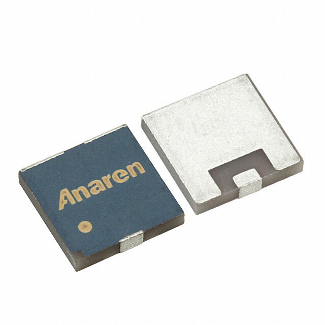
ICGOO电子元器件商城为您提供HMC583LP5E由Hittite设计生产,在icgoo商城现货销售,并且可以通过原厂、代理商等渠道进行代购。 HMC583LP5E价格参考¥208.19-¥208.19。HittiteHMC583LP5E封装/规格:RF 其它 IC 和模块, RF IC VCO General Purpose 11.5GHz ~ 12.8GHz Triple Outputs (Divide by 2, Divide by 4, Standard) 32-QFN (5x5)。您可以下载HMC583LP5E参考资料、Datasheet数据手册功能说明书,资料中有HMC583LP5E 详细功能的应用电路图电压和使用方法及教程。
HMC583LP5E是由Analog Devices Inc.(亚德诺半导体公司)生产的RF(射频)IC,具体属于RF其它IC和模块类别。该器件主要用于无线通信、雷达系统、测试测量设备等高频应用领域。

 应用场景:

1. 无线通信系统:
   - HMC583LP5E适用于各种无线通信基础设施设备,如基站、中继站等。它可以在这些系统中用于信号的放大、调制和解调,确保信号的高效传输和接收。

2. 雷达系统:
   - 在军事和民用雷达系统中,HMC583LP5E可以用于信号处理,特别是在目标检测、跟踪和识别方面。其高性能的射频特性使其能够在复杂电磁环境中保持稳定工作。

3. 测试与测量设备:
   - 该器件广泛应用于各类射频测试仪器中,如频谱分析仪、网络分析仪等。它可以提供精确的信号生成和处理功能,帮助工程师进行性能评估和故障诊断。

4. 卫星通信:
   - 在卫星通信系统中,HMC583LP5E可用于地面站和卫星之间的信号传输,确保数据的可靠性和完整性。其低噪声和高线性度特性使得它在远距离通信中表现出色。

5. 汽车电子:
   - 随着自动驾驶技术的发展,HMC583LP5E也被应用于车载雷达和V2X(车对万物)通信系统中,提高车辆的安全性和智能化水平。

6. 物联网(IoT):
   - 在物联网设备中,HMC583LP5E可以用于连接传感器节点和网关,实现远程监控和数据传输。其低功耗和小尺寸设计使其非常适合嵌入式应用。

总之,HMC583LP5E凭借其卓越的射频性能和可靠性,成为多种高频应用场景中的关键组件。无论是通信基础设施还是高端测试设备,它都能提供稳定的射频信号处理能力,满足不同行业的需求。
| 参数 | 数值 |
| 产品目录 | |
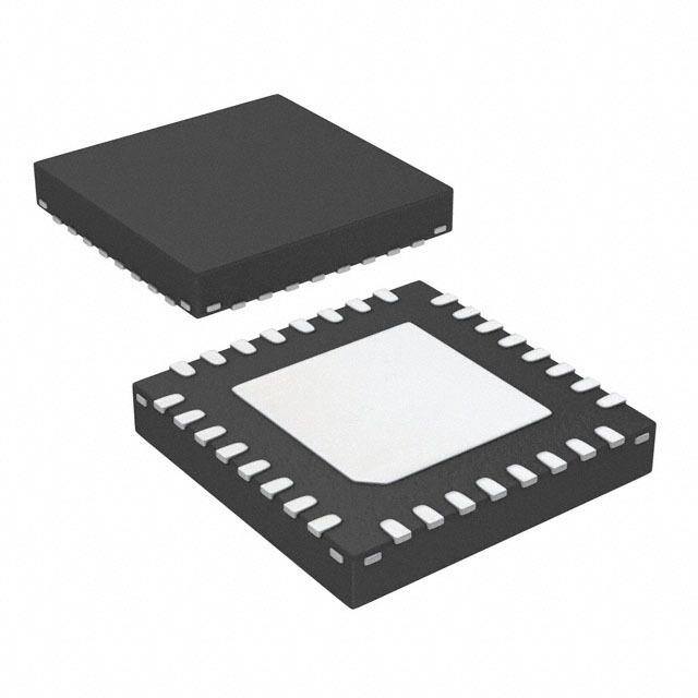
| 描述 | IC MMIC VCO HBT BIPOLAR 32-QFN |
| 产品分类 | |
| 品牌 | Hittite Microwave Corporation |
| 数据手册 | |
| 产品图片 |
|
| 产品型号 | HMC583LP5E |
| RF类型 | 通用 |
| rohs | 无铅 / 符合限制有害物质指令(RoHS)规范要求 |
| 产品系列 | - |
| 供应商器件封装 | 32-SMT (5x5) |
| 其它名称 | 1127-1467 |
| 功能 | VCO |
| 包装 | 剪带 |
| 封装/外壳 | 32-VFQFN 裸露焊盘 |
| 标准包装 | 50 |
| 辅助属性 | 三路输出(除以 2,除以 4,标准) |
| 频率 | 11.5GHz ~ 12.8GHz |


- 商务部:美国ITC正式对集成电路等产品启动337调查
- 曝三星4nm工艺存在良率问题 高通将骁龙8 Gen1或转产台积电
- 太阳诱电将投资9.5亿元在常州建新厂生产MLCC 预计2023年完工
- 英特尔发布欧洲新工厂建设计划 深化IDM 2.0 战略
- 台积电先进制程称霸业界 有大客户加持明年业绩稳了
- 达到5530亿美元!SIA预计今年全球半导体销售额将创下新高
- 英特尔拟将自动驾驶子公司Mobileye上市 估值或超500亿美元
- 三星加码芯片和SET,合并消费电子和移动部门,撤换高东真等 CEO
- 三星电子宣布重大人事变动 还合并消费电子和移动部门
- 海关总署:前11个月进口集成电路产品价值2.52万亿元 增长14.8%


PDF Datasheet 数据手册内容提取
HMC583LP5 583LP5E / v03.1210 MMIC VCO w/ HALF FREQUENCY OUTPUT & DIVIDE-BY-4, 11.5 - 12.8 GHz Typical Applications Features Low noise MMIC VCO w/Half Frequency, Divide-by-4 Dual Output: Fo = 11.5 - 12.8 GHz Outputs for: Fo/2 = 5.75 - 6.4 GHz • Point to Point/Multipoint Radio Pout: +11 dBm • Test Equipment & Industrial Controls Phase Noise: -110 dBc/Hz @100 kHz Typ. • SATCOM No External Resonator Needed • Military End-Use 32 Lead 5x5mm SMT Package: 25mm² Functional Diagram General Description The HMC583LP5 & HMC583LP5E are GaAs InGaP Heterojunction Bipolar Transistor (HBT) MMIC VCOs. The HMC583LP5 & HMC583LP5E integrate resona- tors, negative resistance devices, varactor diodes and feature half frequency and divide-by-4 outputs. The VCO’s phase noise performance is excellent over temperature, shock, and process due to the oscillator’s 8 monolithic structure. Power output is +11 dBm typical from a +5V supply voltage. The prescaler and RF/2 functions can be disabled to conserve current if not required. The voltage controlled oscillator is packaged T M in a leadless QFN 5x5 mm surface mount package, and requires no external matching components. S - T U P Electrical Specifications, T = +25° C, Vcc (Dig), Vcc (Amp), Vcc (RF) = +5V T A U Parameter Min. Typ. Max. Units O Fo 11.5 - 12.8 GHz Frequency Range Fo/2 5.75 - 6.4 GHz 2 RFOUT +7 +13 dBm / o Power Output RFOUT/2 +9 +15 dBm F RFOUT/4 -9 -3 dBm SSB Phase Noise @ 100 kHz Offset, h -110 dBc/Hz Vtune= +5V @ RFOUT t wi Tune Voltage Vtune 2 12 V Supply Current Icc(Dig) + Icc(Amp) + Icc(RF) 310 350 390 mA S Tune Port Leakage Current (Vtune= 12V) 10 µA O Output Return Loss 2 dB C Harmonics/Subharmonics V 1/2 26 dBc 2nd 22 dBc 3rd 30 dBc Pulling (into a 2.0:1 VSWR) 3 MHz pp Pushing @ Vtune= 5V 20 MHz/V Frequency Drift Rate 1.0 MHz/°C InforFmaotiro np fruircniseh,e dd beyl iAvnealroyg Daenvidce st ois pbelaliecveed otor dbee arcsc:u rHateit taintde reMliaibcler. oHwowaevveer, Cnoo rpFoorr aptriiocen,, d2e0liv Aerlyp, haand R too apdla,c Ce horedlemrss: fAonrdal,o gM DAe v0ic1e8s2, 4Inc., responsibility is assumed by Analog Devices for its use, nor for any infringements of patents or other One Technology Way, P.O. Box 9106, Norwood, MA 02062-9106 8 - 1 rliicgehntss eo fi sth girrda nptaerdti ebsy t himatp mlicaaPyt iorhenso uonlrt ofertoh:m e9r wit7sis 8ues -eu2.n dS5ep0re ca-inf3iyc 3aptia4otne3sn ts ou rb jpeFacttae tnoxt c:r hig9ahn7tgs 8eo wf- 2Aithn5oau0lot g-n 3oDti3ecve7i.c 3eNso . POhrodnee:r 7 O81n-3-l2i9n-e4 7a0t0 w(cid:127) wOrwde.hr oitntliitnee. cato wmww.analog.com Trademarks and registered trademarks arAe tphep plriocpearttyi oof nth eSir urepsppecotivret :o wPnehrso.ne: 978-250-3A3p4p3li c aotrio na Spuppsp@orht: iPtthitoen.ec: o1-m800-ANALOG-D
HMC583LP5 / 583LP5E v03.1210 MMIC VCO w/ HALF FREQUENCY OUTPUT & DIVIDE-BY-4, 11.5 - 12.8 GHz Frequency vs. Tuning Voltage, Vcc = +5V Frequency vs. Tuning Voltage, T= 25°C 13.6 13.6 z) z) H H G12.6 G12.6 Y ( Y ( C C N N E E U U Q11.6 Q11.6 E E R R F F T +25C T 4.75V TPU10.6 +-4805CC TPU10.6 55..0205VV U U O O 9.6 9.6 0 1 2 3 4 5 6 7 8 9 10 11 12 13 0 1 2 3 4 5 6 7 8 9 10 11 12 13 TUNING VOLTAGE (VOLTS) TUNING VOLTAGE (VOLTS) Output Power Sensitivity vs. Tuning Voltage, Vcc = +5V vs. Tuning Voltage, Vcc = +5V 700 16 600 14 8 +25C Hz/Volt)500 +-4805CC R (dBm) 1102 SITIVITY (M340000 PUT POWE 68 +25C MT SEN200 OUT 4 +-4805CC S 100 2 - T 0 0 0 1 2 3 4 5 6 7 8 9 10 11 12 13 0 1 2 3 4 5 6 7 8 9 10 11 12 13 U TUNING VOLTAGE (VOLTS) TUNING VOLTAGE (VOLTS) P T U O SSB Phase Noise vs. Tuning Voltage SSB Phase Noise @ Vtune = +5V 2 -70 0 / -20 o OISE (dBc/Hz) --9800 1 0100kkHHzz OOFFFFSSEETT OISE (dBc/Hz) ---864000 ++-428055CCC Fwith N N SE -100 SE -100 A A S H H-120 SB P-110 SB P-140 O S S C -160 V -120 -180 0 1 2 3 4 5 6 7 8 9 10 11 12 13 103 104 105 106 107 TUNING VOLTAGE (VOLTS) OFFSET FREQUENCY (Hz) InforFmaotiro np fruircniseh,e dd beyl iAvnealroyg Daenvidce st ois pbelaliecveed otor dbee arcsc:u rHateit taintde reMliaibcler. oHwowaevveer, Cnoo rpFoorr aptriiocen,, d2e0liv Aerlyp, haand R too apdla,c Ce horedlemrss: fAonrdal,o gM DAe v0ic1e8s2, 4Inc., responsibility is assumed by Analog Devices for its use, nor for any infringements of patents or other One Technology Way, P.O. Box 9106, Norwood, MA 02062-9106 rights of third parties that maPy rhesounlt fero:m 9 it7s 8us-e2. S5p0ec-if3ic3ati4on3s s u b jeFcta tox c: h9an7g8e w-2ith5ou0t -n3oti3ce7. 3No POhrodnee:r 7 O81n-3-l2i9n-e4 7a0t0 w(cid:127) wOrwde.hr oitntliitnee. cato wmww.analog.com 8 - 2 license is granted by implication or otherwise under any patent or patent rights of Analog Devices. Trademarks and registered trademarks arAe tphep plriocpearttyi oof nth eSir urepsppecotivret :o wPnehrso.ne: 978-250-3A3p4p3li c aotrio na Spuppsp@orht: iPtthitoen.ec: o1-m800-ANALOG-D
HMC583LP5 / 583LP5E v03.1210 MMIC VCO w/ HALF FREQUENCY OUTPUT & DIVIDE-BY-4, 11.5 - 12.8 GHz RFOUT/2 Frequency RFOUT/2 Output Power vs. Tuning Voltage, Vcc = +5V vs. Tuning Voltage, Vcc = +5V 6.8 16 z) GH 6.4 m) 12 Y ( dB ENC 6 ER ( U W Q O 8 E P T FR 5.6 PUT +25C U T +85C UTP 5.2 ++2855CC OU 4 -40C O -40C 4.8 0 0 1 2 3 4 5 6 7 8 9 10 11 12 13 0 1 2 3 4 5 6 7 8 9 10 11 12 13 TUNING VOLTAGE (VOLTS) TUNING VOLTAGE (VOLTS) Divide-by-4 Frequency Divide-by-4 Output Power vs. Tuning Voltage, Vcc = +5V vs. Tuning Voltage, Vcc = +5V 3.4 0 8 GHz) 3.2 m) -2 ++2855CC Y ( dB -40C ENC 3 ER ( -4 U W T EQ PO M T FR 2.8 PUT -6 S PU +25C UT OUT 2.6 +-4805CC O -8 - T 2.4 -10 U 0 1 2 3 4 5 6 7 8 9 10 11 12 13 0 1 2 3 4 5 6 7 8 9 10 11 12 13 P TUNING VOLTAGE (VOLTS) TUNING VOLTAGE (VOLTS) T U O Absolute Maximum Ratings Typical Supply Current vs. Vcc 2 Vcc(Dig), Vcc(Amp), Vcc(RF) +5.5 Vdc Vcc (V) Icc (mA) / o Vtune 0 to +15V 4.75 320 F Junction Temperature 135 °C 5.00 350 h Continuous Pdiss (T=85 °C) 5.25 380 t 2.17 W i (derate 43.5 mW/C above 85 °C Note: VCO will operate over full voltage range shown above. w Thermal Resistance 23 °C/W S (junction to ground paddle) ELECTROSTATIC SENSITIVE DEVICE O Storage Temperature -65 to +150 °C OBSERVE HANDLING PRECAUTIONS C Operating Temperature -40 to +85 °C V ESD Sensitivity (HBM) Class 1A InforFmaotiro np fruircniseh,e dd beyl iAvnealroyg Daenvidce st ois pbelaliecveed otor dbee arcsc:u rHateit taintde reMliaibcler. oHwowaevveer, Cnoo rpFoorr aptriiocen,, d2e0liv Aerlyp, haand R too apdla,c Ce horedlemrss: fAonrdal,o gM DAe v0ic1e8s2, 4Inc., responsibility is assumed by Analog Devices for its use, nor for any infringements of patents or other One Technology Way, P.O. Box 9106, Norwood, MA 02062-9106 8 - 3 rliicgehntss eo fi sth girrda nptaerdti ebsy t himatp mlicaaPyt iorhenso uonlrt ofertoh:m e9r wit7sis 8ues -eu2.n dS5ep0re ca-inf3iyc 3aptia4otne3sn ts ou rb jpeFacttae tnoxt c:r hig9ahn7tgs 8eo wf- 2Aithn5oau0lot g-n 3oDti3ecve7i.c 3eNso . POhrodnee:r 7 O81n-3-l2i9n-e4 7a0t0 w(cid:127) wOrwde.hr oitntliitnee. cato wmww.analog.com Trademarks and registered trademarks arAe tphep plriocpearttyi oof nth eSir urepsppecotivret :o wPnehrso.ne: 978-250-3A3p4p3li c aotrio na Spuppsp@orht: iPtthitoen.ec: o1-m800-ANALOG-D
HMC583LP5 / 583LP5E v03.1210 MMIC VCO w/ HALF FREQUENCY OUTPUT & DIVIDE-BY-4, 11.5 - 12.8 GHz Outline Drawing NOTES: 1. LEADFRAME MATERIAL: COPPER ALLOY 2. DIMENSIONS ARE IN INCHES [MILLIMETERS] 3. LEAD SPACING TOLERANCE IS NON-CUMULATIVE. 8 4. PAD BURR LENGTH SHALL BE 0.15mm MAXIMUM. PAD BURR HEIGHT SHALL BE 0.05mm MAXIMUM. 5. PACKAGE WARP SHALL NOT EXCEED 0.05mm. 6. ALL GROUND LEADS AND GROUND PADDLE MUST BE SOLDERED TO PCB RF GROUND. T 7. REFER TO HITTITE APPLICATION NOTE FOR SUGGESTED LAND PATTERN. Package Information M S Part Number Package Body Material Lead Finish MSL Rating Package Marking [3] HMC583LP5 Low Stress Injection Molded Plastic Sn/Pb Solder MSL3 [1] H583 - XXXX T HMC583LP5E RoHS-compliant Low Stress Injection Molded Plastic 100% matte Sn MSL3 [2] H583 U XXXX P [1] Max peak reflow temperature of 235 °C T [2] Max peak reflow temperature of 260 °C U [3] 4-Digit lot number XXXX O Pin Descriptions 2 / Pin Number Function Description Interface Schematic o 1 - 3, 8 - 10, 13 - 18, No Connection. These pins may be connected to RF/ F N/C 20, 22 - 28, 30 - 32 DC ground. Performance will not be affected. h t i w Divide-by-4 output. 4 RFOUT/4 DC block required. S O C V Supply voltage for prescaler. If prescaler is not 6 Vcc (Dig) required, this pin may be left open to conserve approxi- mately 65 mA of current. InforFmaotiro np fruircniseh,e dd beyl iAvnealroyg Daenvidce st ois pbelaliecveed otor dbee arcsc:u rHateit taintde reMliaibcler. oHwowaevveer, Cnoo rpFoorr aptriiocen,, d2e0liv Aerlyp, haand R too apdla,c Ce horedlemrss: fAonrdal,o gM DAe v0ic1e8s2, 4Inc., responsibility is assumed by Analog Devices for its use, nor for any infringements of patents or other One Technology Way, P.O. Box 9106, Norwood, MA 02062-9106 rights of third parties that maPy rhesounlt fero:m 9 it7s 8us-e2. S5p0ec-if3ic3ati4on3s s u b jeFcta tox c: h9an7g8e w-2ith5ou0t -n3oti3ce7. 3No POhrodnee:r 7 O81n-3-l2i9n-e4 7a0t0 w(cid:127) wOrwde.hr oitntliitnee. cato wmww.analog.com 8 - 4 license is granted by implication or otherwise under any patent or patent rights of Analog Devices. Trademarks and registered trademarks arAe tphep plriocpearttyi oof nth eSir urepsppecotivret :o wPnehrso.ne: 978-250-3A3p4p3li c aotrio na Spuppsp@orht: iPtthitoen.ec: o1-m800-ANALOG-D
HMC583LP5 / 583LP5E v03.1210 MMIC VCO w/ HALF FREQUENCY OUTPUT & DIVIDE-BY-4, 11.5 - 12.8 GHz Pin Descriptions Pin Number Function Description Interface Schematic Supply voltage, for RFOUT/2 output. If RFOUT/2 7 Vcc (Amp) is not required, this pin may be left open to conserve approximately 30 mA of current. 12 RFOUT/2 Half frequency output (AC coupled). 19 RF OUT RF output (AC coupled). 8 21 Vcc (RF) Supply Voltage, +5V Control voltage and modulation input. Modulation T bandwidth dependent on drive source impedance. See M 29 VTUNE “Determining the FM Bandwidth of a Wideband Varac- S tor Tuned VCO” application note. - Package bottom has an exposed metal paddle that T 5, 11, Paddle GND must be connected to RF/DC ground. U Typical Application Circuit P T U O 2 / o F h t i w S O C V InforFmaotiro np fruircniseh,e dd beyl iAvnealroyg Daenvidce st ois pbelaliecveed otor dbee arcsc:u rHateit taintde reMliaibcler. oHwowaevveer, Cnoo rpFoorr aptriiocen,, d2e0liv Aerlyp, haand R too apdla,c Ce horedlemrss: fAonrdal,o gM DAe v0ic1e8s2, 4Inc., responsibility is assumed by Analog Devices for its use, nor for any infringements of patents or other One Technology Way, P.O. Box 9106, Norwood, MA 02062-9106 8 - 5 rliicgehntss eo fi sth girrda nptaerdti ebsy t himatp mlicaaPyt iorhenso uonlrt ofertoh:m e9r wit7sis 8ues -eu2.n dS5ep0re ca-inf3iyc 3aptia4otne3sn ts ou rb jpeFacttae tnoxt c:r hig9ahn7tgs 8eo wf- 2Aithn5oau0lot g-n 3oDti3ecve7i.c 3eNso . POhrodnee:r 7 O81n-3-l2i9n-e4 7a0t0 w(cid:127) wOrwde.hr oitntliitnee. cato wmww.analog.com Trademarks and registered trademarks arAe tphep plriocpearttyi oof nth eSir urepsppecotivret :o wPnehrso.ne: 978-250-3A3p4p3li c aotrio na Spuppsp@orht: iPtthitoen.ec: o1-m800-ANALOG-D
HMC583LP5 / 583LP5E v03.1210 MMIC VCO w/ HALF FREQUENCY OUTPUT & DIVIDE-BY-4, 11.5 - 12.8 GHz Evaluation PCB 8 T M S - T U P T U O List of Materials for Evaluation PCB 110227 [1] The circuit board used in the application should use 2 Item Description / RF circuit design techniques. Signal lines should o J1 - J4 PCB Mount SMA RF Connector have 50 Ohm impedance while the package ground F J5 - J6 2 mm DC Header leads and backside ground paddle should be con- h C1 - C3 100 pF Capacitor, 0402 Pkg. t nected directly to the ground plane similar to that C4 1,000 pF Capacitor, 0402 Pkg. wi shown. A sufficient number of via holes should be C5 - C7 2.2 µF Tantalum Capacitor used to connect the top and bottom ground planes. S U1 HMC583LP5 / HMC583LP5E VCO The evaluation circuit board shown is available from O PCB [2] 110225 Eval Board Hittite upon request. C [1] Reference this number when ordering complete evaluation PCB V [2] Circuit Board Material: Rogers 4350 InforFmaotiro np fruircniseh,e dd beyl iAvnealroyg Daenvidce st ois pbelaliecveed otor dbee arcsc:u rHateit taintde reMliaibcler. oHwowaevveer, Cnoo rpFoorr aptriiocen,, d2e0liv Aerlyp, haand R too apdla,c Ce horedlemrss: fAonrdal,o gM DAe v0ic1e8s2, 4Inc., responsibility is assumed by Analog Devices for its use, nor for any infringements of patents or other One Technology Way, P.O. Box 9106, Norwood, MA 02062-9106 rights of third parties that maPy rhesounlt fero:m 9 it7s 8us-e2. S5p0ec-if3ic3ati4on3s s u b jeFcta tox c: h9an7g8e w-2ith5ou0t -n3oti3ce7. 3No POhrodnee:r 7 O81n-3-l2i9n-e4 7a0t0 w(cid:127) wOrwde.hr oitntliitnee. cato wmww.analog.com 8 - 6 license is granted by implication or otherwise under any patent or patent rights of Analog Devices. Trademarks and registered trademarks arAe tphep plriocpearttyi oof nth eSir urepsppecotivret :o wPnehrso.ne: 978-250-3A3p4p3li c aotrio na Spuppsp@orht: iPtthitoen.ec: o1-m800-ANALOG-D