首页 > HMC394LP4E > 详情
 Datasheet下载
- 型号: HMC394LP4E
- 制造商: Hittite
- 库位|库存: xxxx|xxxx
- 要求:
| 数量阶梯 | 香港交货 | 国内含税 |
| +xxxx | $xxxx | ¥xxxx |
查看当月历史价格
查看今年历史价格
产品参数
| 参数 | 数值 |
| 产品目录 | 射频/IF 和 RFID |
| 描述 | RF HBT PROG 5BIT COUNTER 24SMT |
| 产品分类 | RF 其它 IC 和模块 |
| 品牌 | Hittite Microwave Corporation |
| 数据手册 | 点击此处下载产品Datasheet |
| 产品图片 |  |
| 产品型号 | HMC394LP4E |
| RF类型 | 通用 |
| rohs | 无铅 / 符合限制有害物质指令(RoHS)规范要求 |
| 产品系列 | - |
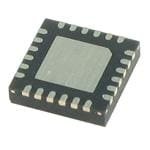
| 供应商器件封装 | 24-QFN(4x4) |
| 其它名称 | 1127-1185-6 |
| 功能 | 计数器 |
| 包装 | Digi-Reel® |
| 封装/外壳 | 24-VQFN 裸露焊盘 |
| 标准包装 | 1 |
| 辅助属性 | - |
| 频率 | 0Hz ~ 2.2GHz |
Datasheet
PDF Datasheet 数据手册内容提取
HMC394LP4 394LP4E / v09.0114 GaAs HBT PROGRAMMABLE 5-BIT COUNTER, DC - 2.2 GHz Typical Applications Features 4 4 Programmable divider for offset synthesizer SSB Phase Noise: -153 dBc/Hz @ 100 kHz and variable divide by N applications: Selectable Division from 2 to 32 • Satellite Communication Systems Parallel 5-Bit Control t t • Point-to-Point and Point-to-Multi-Point Radios M Wide Input Power Range: -20 to +10 dBm M • LMDS s 24 Lead 4x4mm QFN Package: 9 mm² s • SONET - - s s r Functional Diagram General Description r o o t The HMC394LP4 & HMC394LP4E are low noise t c GaAs HBT programmable 5-bit counters in 4 x c e 4mm leadless surface mount packages. This device e t allows continuous division from N= 2 to 32 at input t e e frequencies up to 2.2 GHz. The output voltage swing is D D 800 mV with a duty cycle inversely proportional to N. & The low additive SSB phase noise of -153 dBc/Hz at & 100 KHz offset makes this counter an excellent choice s s r for low noise synthesizer applications. r e e D D i i v v i i D D y y c c n n e e u u q Electrical Specifications, T = +25° C, 50 Ohm System, Vcc= 5V q A e e Parameter Conditions Min. Typ. Max. Units r r Maximum Input Frequency 2.2 GHz F F Minimum Input Frequency Sine Wave Input [1] 0.1 GHz Input Power Range Fin = 0.1 to 2.2 GHz -15 >-20 +10 dBm Output Power Divide-by-2 4 dBm SSB Phase Noise Fin = 1 GHz, N = 4 -153 dBc/Hz Output Transition Time 100 ps Supply Current (Icc) 194 mA 1. Divider will operate down to DC for square-wave input signal. InforFmaotiro np fruircniseh,e dd beyl iAvnealroyg Daenvidce st ois pbelaliecveed otor dbee arcsc:u rHateit taintde reMliaibcler. oHwowaevveer, Cnoo rpFoorr aptriiocen,, d2e0liv Aerlyp, haand R too apdla,c Ce horedlemrss: fAonrdal,o gM DAe v0ic1e8s2, 4Inc., responsibility is assumed by Analog Devices for its use, nor for any infringements of patents or other One Technology Way, P.O. Box 9106, Norwood, MA 02062-9106 4 - 1 rliicgehntss eo fi sth girrda nptaerdti ebsy t himatp mlicaaPyt iorhenso uonlrt ofertoh:m e9r wit7sis 8ues -eu2.n dS5ep0re ca-inf3iyc 3aptia4otne3sn ts ou rb jpeFacttae tnoxt c:r hig9ahn7tgs 8eo wf- 2Aithn5oau0lot g-n 3oDti3ecve7i.c 3eNso . POhrodnee:r 7 O81n-3-2li9n-e4 7a0t0 w(cid:127) wOrwde.hr oitntliitnee. cato wmww.analog.com Trademarks and registered trademarks arAe tphep plriocpearttyi oof nth eSir urepsppecotivret :o wPnehrso.ne: 978-250-3A3p4p3li c aotrio na Spuppsp@orht: iPtthitoen.ec: o1-m800-ANALOG-D
HMC394LP4 / 394LP4E v09.0114 GaAs HBT PROGRAMMABLE 5-BIT COUNTER, DC - 2.2 GHz Input Sensitivity Window, 5 major Input Sensitivity Window vs. Divide Ratio States, T= 25 °C Temperature, N= 16, T= -40 °C to +85 °C 4 4 20 20 10 10 m) m) B B t R (d 0 R (d 0 t M E Recommended E M W W O Operating Window O s UT P-10 UT P-10 s s - INP-20 INP-20 s - r r o -30 -30 o 0 0.5 1 1.5 2 2.5 3 0 0.5 1 1.5 2 2.5 3 t t INPUT FREQUENCY (GHz) INPUT FREQUENCY (GHz) c c e e t Output Power, 5 Major Divide SSB Phase Noise Performance, t e Ratio States, T= 25 °C Fin= 1 GHz, N= 4, T= 25 °C e D D 10 -60 & N=2 N=4 -70 & ers wer (dBm) -505 N=8 OISE (dBc/Hz)--11--10980000 ers viD Output Po-10 N=16 PHASE N--113200 viD Di -15 N=32 SSB -140 Di -150 y -20 -160 y c 0.4 0.6 0.8 1 1.2 1.4 1.6 1.8 2 2.2 2.4 102 103 104 105 106 107 c n INPUT FREQUENCY (GHz) OFFSET FREQUENCY (Hz) n e e u Fundamental Feedthru Power, u q Pin= 0 dBm, T= 25 °C Typical Supply Current vs. Vcc q e e 0 Vcc (V) Icc (mA) r r 4.75 176 F F -10 m) 5.0 194 B d 5.25 210 L (-20 E Note: Divider will operate over full voltage range shown V E above. L T -30 U P UT N=2 O N=4 -40 N=8 N=16 N=32 -50 0.4 0.6 0.8 1 1.2 1.4 1.6 1.8 2 2.2 2.4 INPUT FREQUENCY (GHz) InforFmaotiro np fruircniseh,e dd beyl iAvnealroyg Daenvidce st ois pbelaliecveed otor dbee arcsc:u rHateit taintde reMliaibcler. oHwowaevveer, Cnoo rpFoorr aptriiocen,, d2e0liv Aerlyp, haand R too apdla,c Ce horedlemrss: fAonrdal,o gM DAe v0ic1e8s2, 4Inc., responsibility is assumed by Analog Devices for its use, nor for any infringements of patents or other One Technology Way, P.O. Box 9106, Norwood, MA 02062-9106 rights of third parties that maPy rhesounlt fero:m 9 it7s 8us-e2. S5p0ec-if3ic3ati4on3s s u b jeFcta tox c: h9an7g8e w-2ith5ou0t -n3oti3ce7. 3No POhrodnee:r 7 O81n-3-2li9n-e4 7a0t0 w(cid:127) wOrwde.hr oitntliitnee. cato wmww.analog.com 4 - 2 license is granted by implication or otherwise under any patent or patent rights of Analog Devices. Trademarks and registered trademarks arAe tphep plriocpearttyi oof nth eSir urepsppecotivret :o wPnehrso.ne: 978-250-3A3p4p3li c aotrio na Spuppsp@orht: iPtthitoen.ec: o1-m800-ANALOG-D
HMC394LP4 / 394LP4E v09.0114 GaAs HBT PROGRAMMABLE 5-BIT COUNTER, DC - 2.2 GHz 2nd Harmonic, 3rd Harmonic, Pin= 0 dBm, T= 25 °C Pin= 0 dBm, T= 25 °C 4 4 0 0 N=2 N=4 N=8 m) -5 m) -5 B B t d d t L ( L ( M E E M EV-10 EV-10 s T L T L s U U - OUTP-15 NN==48 NN==1362 OUTP-15 N=32 N=16 - s s r r o -20 -20 o 0.4 0.6 0.8 1 1.2 1.4 1.6 1.8 2 2.2 2.4 0.4 0.6 0.8 1 1.2 1.4 1.6 1.8 2 2.2 2.4 t t INPUT FREQUENCY (GHz) INPUT FREQUENCY (GHz) c c e e t 4th Harmonic, 5th Harmonic, t e Pin= 0 dBm, T= 25 °C Pin= 0 dBm, T= 25 °C e D D 0 0 & N=2 N=16 & -5 N=8 N=32 -5 s m) m) s r dB-10 dB-10 r L ( L ( e E E e EV-15 EV-15 D L L D T T vi TPU-20 TPU-20 vi U U Di O-25 O-25 NN==24 NN==1362 Di N=8 y -30 -30 y c 0.4 0.6 0.8 1 1.2 1.4 1.6 1.8 2 2.2 2.4 0.4 0.6 0.8 1 1.2 1.4 1.6 1.8 2 2.2 2.4 c n INPUT FREQUENCY (GHz) INPUT FREQUENCY (GHz) n e e u Output Voltage Wavform, Fin= 1 GHz, Output Voltage Wavform, Fin= 1 GHz, u q N= 2, Pin= 0 dBm, T= 25 °C N= 17, Pin= 0 dBm, T= 25 °C q e e 300 500 r r F 200 400 F V)100 V)300 m m E ( E ( UD 0 UD200 MPLIT-100 MPLIT100 A A -200 0 -300 -100 38 38.5 39 39.5 40 40.5 41 48 50 52 54 56 58 60 62 64 66 68 70 TIME (nS) TIME (nS) InforFmaotiro np fruircniseh,e dd beyl iAvnealroyg Daenvidce st ois pbelaliecveed otor dbee arcsc:u rHateit taintde reMliaibcler. oHwowaevveer, Cnoo rpFoorr aptriiocen,, d2e0liv Aerlyp, haand R too apdla,c Ce horedlemrss: fAonrdal,o gM DAe v0ic1e8s2, 4Inc., responsibility is assumed by Analog Devices for its use, nor for any infringements of patents or other One Technology Way, P.O. Box 9106, Norwood, MA 02062-9106 4 - 3 rliicgehntss eo fi sth girrda nptaerdti ebsy t himatp mlicaaPyt iorhenso uonlrt ofertoh:m e9r wit7sis 8ues -eu2.n dS5ep0re ca-inf3iyc 3aptia4otne3sn ts ou rb jpeFacttae tnoxt c:r hig9ahn7tgs 8eo wf- 2Aithn5oau0lot g-n 3oDti3ecve7i.c 3eNso . POhrodnee:r 7 O81n-3-2li9n-e4 7a0t0 w(cid:127) wOrwde.hr oitntliitnee. cato wmww.analog.com Trademarks and registered trademarks arAe tphep plriocpearttyi oof nth eSir urepsppecotivret :o wPnehrso.ne: 978-250-3A3p4p3li c aotrio na Spuppsp@orht: iPtthitoen.ec: o1-m800-ANALOG-D
HMC394LP4 / 394LP4E v09.0114 GaAs HBT PROGRAMMABLE 5-BIT COUNTER, DC - 2.2 GHz Absolute Maximum Ratings RF Input (Vcc = +5V) +13 dBm 4 4 Vcc +5.5V ELECTROSTATIC SENSITIVE DEVICE VLogic -1.6 to -1.2 Vcc OBSERVE HANDLING PRECAUTIONS Maximum Channel Temperature 135 °C t Continuous Pdiss (T = 85 °C) t 1.155 W M (derate 55 mW/°C above 85 °C) M s Thermal Resistance (u j-c ) Junction to 21.5 °C/W s Case (Ground Paddle) - - Storage Temperature -65 to +150°C s s r Operating Temperature +55 to +85°C r o o t Outline Drawing t c c e e t t e e D D & & s s r r e e D D i i v v i i D D y y c c n n e NOTES: e u 1. LEADFRAME MATERIAL: COPPER ALLOY u 2. DIMENSIONS ARE IN INCHES [MILLIMETERS] q q 3. LEAD SPACING TOLERANCE IS NON-CUMULATIVE. e 4. PAD BURR LENGTH SHALL BE 0.15mm MAXIMUM. e r PAD BURR HEIGHT SHALL BE 0.05mm MAXIMUM. r 5. PACKAGE WARP SHALL NOT EXCEED 0.05mm. F F 6. ALL GROUND LEADS AND GROUND PADDLE MUST BE SOLDERED TO PCB RF GROUND. 7. REFER TO HITTITE APPLICATION NOTE FOR SUGGESTED LAND PATTERN. Package Information Part Number Package Body Material Lead Finish MSL Rating Package Marking [3] HMC394LP4 Low Stress Injection Molded Plastic Sn/Pb Solder MSL1 [1] H394 XXXX HMC394LP4E RoHS-compliant Low Stress Injection Molded Plastic 100% matte Sn MSL1 [2] H394 XXXX [1] Max peak reflow temperature of 235 °C [2] Max peak reflow temperature of 260 °C [3] 4-Digit lot number XXXX InforFmaotiro np fruircniseh,e dd beyl iAvnealroyg Daenvidce st ois pbelaliecveed otor dbee arcsc:u rHateit taintde reMliaibcler. oHwowaevveer, Cnoo rpFoorr aptriiocen,, d2e0liv Aerlyp, haand R too apdla,c Ce horedlemrss: fAonrdal,o gM DAe v0ic1e8s2, 4Inc., responsibility is assumed by Analog Devices for its use, nor for any infringements of patents or other One Technology Way, P.O. Box 9106, Norwood, MA 02062-9106 rights of third parties that maPy rhesounlt fero:m 9 it7s 8us-e2. S5p0ec-if3ic3ati4on3s s u b jeFcta tox c: h9an7g8e w-2ith5ou0t -n3oti3ce7. 3No POhrodnee:r 7 O81n-3-2li9n-e4 7a0t0 w(cid:127) wOrwde.hr oitntliitnee. cato wmww.analog.com 4 - 4 license is granted by implication or otherwise under any patent or patent rights of Analog Devices. Trademarks and registered trademarks arAe tphep plriocpearttyi oof nth eSir urepsppecotivret :o wPnehrso.ne: 978-250-3A3p4p3li c aotrio na Spuppsp@orht: iPtthitoen.ec: o1-m800-ANALOG-D
HMC394LP4 / 394LP4E v09.0114 GaAs HBT PROGRAMMABLE 5-BIT COUNTER, DC - 2.2 GHz Pin Description 4 4 Pin Number Function Description Interface Schematic t t M M 1 - 5 AO - A4 CMOS compatible control input bit 0 (LSB) - 4. s s - - s s r r o o 6, 9, 10, 11, t Ground: Backside of package has exposed metal ground slug which t 12, 15, 18, GND must be connected to ground. c 19, 20, 21, 22 c e e t t e 7, 8, 23, 24 VCC Supply voltage 5V ± 0.25V must be applied to all four pins. e D D & & s s r 13 IN RF input 180° out of phase with pin 14 must be AC ground. r e e D D i i v v i i D D y 14 IN RF input must be DC blocked. y c c n n e e u u q 16 OUT Divided output pulse. q e e r r F F 17 OUT Divided output pulse 180° out of phase with pin 16. InforFmaotiro np fruircniseh,e dd beyl iAvnealroyg Daenvidce st ois pbelaliecveed otor dbee arcsc:u rHateit taintde reMliaibcler. oHwowaevveer, Cnoo rpFoorr aptriiocen,, d2e0liv Aerlyp, haand R too apdla,c Ce horedlemrss: fAonrdal,o gM DAe v0ic1e8s2, 4Inc., responsibility is assumed by Analog Devices for its use, nor for any infringements of patents or other One Technology Way, P.O. Box 9106, Norwood, MA 02062-9106 4 - 5 rliicgehntss eo fi sth girrda nptaerdti ebsy t himatp mlicaaPyt iorhenso uonlrt ofertoh:m e9r wit7sis 8ues -eu2.n dS5ep0re ca-inf3iyc 3aptia4otne3sn ts ou rb jpeFacttae tnoxt c:r hig9ahn7tgs 8eo wf- 2Aithn5oau0lot g-n 3oDti3ecve7i.c 3eNso . POhrodnee:r 7 O81n-3-2li9n-e4 7a0t0 w(cid:127) wOrwde.hr oitntliitnee. cato wmww.analog.com Trademarks and registered trademarks arAe tphep plriocpearttyi oof nth eSir urepsppecotivret :o wPnehrso.ne: 978-250-3A3p4p3li c aotrio na Spuppsp@orht: iPtthitoen.ec: o1-m800-ANALOG-D
HMC394LP4 / 394LP4E v09.0114 GaAs HBT PROGRAMMABLE 5-BIT COUNTER, DC - 2.2 GHz HMC394LP4 Programming Truth Table 4 4 (LSB) Function A1 A2 A3 A4 A0 Output Low 0 0 0 0 0 / 2 1 0 0 0 0 t t / 3 0 1 0 0 0 M M / 4 1 1 0 0 0 s s - - - - - - - - / 32 1 1 1 1 1 s s Note: A0 through A4 are CMOS compatible logic control inputs. r r o o t t c c e e t t e Application Circuit, (2 GHz - Divide-by-20) e D D & & s s r r e e D D i i v v i i D D y y c c n n e e u u q q e e r r F F * Note: Mount bypass capacitors as close to pins as possible. InforFmaotiro np fruircniseh,e dd beyl iAvnealroyg Daenvidce st ois pbelaliecveed otor dbee arcsc:u rHateit taintde reMliaibcler. oHwowaevveer, Cnoo rpFoorr aptriiocen,, d2e0liv Aerlyp, haand R too apdla,c Ce horedlemrss: fAonrdal,o gM DAe v0ic1e8s2, 4Inc., responsibility is assumed by Analog Devices for its use, nor for any infringements of patents or other One Technology Way, P.O. Box 9106, Norwood, MA 02062-9106 rights of third parties that maPy rhesounlt fero:m 9 it7s 8us-e2. S5p0ec-if3ic3ati4on3s s u b jeFcta tox c: h9an7g8e w-2ith5ou0t -n3oti3ce7. 3No POhrodnee:r 7 O81n-3-2li9n-e4 7a0t0 w(cid:127) wOrwde.hr oitntliitnee. cato wmww.analog.com 4 - 6 license is granted by implication or otherwise under any patent or patent rights of Analog Devices. Trademarks and registered trademarks arAe tphep plriocpearttyi oof nth eSir urepsppecotivret :o wPnehrso.ne: 978-250-3A3p4p3li c aotrio na Spuppsp@orht: iPtthitoen.ec: o1-m800-ANALOG-D
HMC394LP4 / 394LP4E v09.0114 GaAs HBT PROGRAMMABLE 5-BIT COUNTER, DC - 2.2 GHz Evaluation PCB 4 4 t t M M s s - - s s r r o o t t c c e e t t e e D D & & s s r r e e The circuit board used in the application should use RF circuit design techniques. Signal lines should have 50 D D Ohm impedance while the package ground leads and backside ground slug should be connected directly to i i v the ground plane similar to that shown. A sufficient number of via holes should be used to connect the top and v Di bottom ground planes. The evaluation circuit board shown is available from Hittite upon request. Di y y c c n n e e u List of Materials for HMC394LP4 Evaluation u q Evaluation PCB 104898 [1] PCB Truth Table q e e Item Description Function S1 S2 S3 S4 S5 r r J1 - J3 PCB Mount SMA RF Connector Output Low 0 0 0 0 0 F F C1 - C2 [2] 1.0 µF Tantalum Capacitor / 2 1 0 0 0 0 C3 - C4 [2] .01 µF Capacitor, 0603 Pkg. / 3 0 1 0 0 0 C5 - C8 1000 pF Capacitor, 0603 Pkg. / 4 1 1 0 0 0 R1* Resistor SIP 10 K ohm - - - - - - S1 - S6 Jumper (shunt) 2mm / 32 1 1 1 1 1 HMC394LP4 / HMC394LP4E Note: 0 = Jumper Installed. U1 5-Bit Counter 1 = Jumper Not Installed. PCB 104435 Eval Board Note: The evaluation PCB for the HMC394LP4 contains [1] Reference this number when ordering complete evaluation PCB 10K Ohm pull up resistors for each of the five control inputs A0 through A4. Programming the 31 distinct division ratios [2] Optional components. consists of installing or removing jumpers S1 through S5, as shown above. Jumper S6 must always be installed to provide ground to pin 20. InforFmaotiro np fruircniseh,e dd beyl iAvnealroyg Daenvidce st ois pbelaliecveed otor dbee arcsc:u rHateit taintde reMliaibcler. oHwowaevveer, Cnoo rpFoorr aptriiocen,, d2e0liv Aerlyp, haand R too apdla,c Ce horedlemrss: fAonrdal,o gM DAe v0ic1e8s2, 4Inc., responsibility is assumed by Analog Devices for its use, nor for any infringements of patents or other One Technology Way, P.O. Box 9106, Norwood, MA 02062-9106 4 - 7 rliicgehntss eo fi sth girrda nptaerdti ebsy t himatp mlicaaPyt iorhenso uonlrt ofertoh:m e9r wit7sis 8ues -eu2.n dS5ep0re ca-inf3iyc 3aptia4otne3sn ts ou rb jpeFacttae tnoxt c:r hig9ahn7tgs 8eo wf- 2Aithn5oau0lot g-n 3oDti3ecve7i.c 3eNso . POhrodnee:r 7 O81n-3-2li9n-e4 7a0t0 w(cid:127) wOrwde.hr oitntliitnee. cato wmww.analog.com Trademarks and registered trademarks arAe tphep plriocpearttyi oof nth eSir urepsppecotivret :o wPnehrso.ne: 978-250-3A3p4p3li c aotrio na Spuppsp@orht: iPtthitoen.ec: o1-m800-ANALOG-D
HMC394LP4 / 394LP4E v09.0114 GaAs HBT PROGRAMMABLE 5-BIT COUNTER, DC - 2.2 GHz Applications Information 4 4 Simplified Block Diagram t t M M s s - - s s r r o o t t c c e e t t e e D D & & s s r r e e D D i i v v Asynchronous Programming i i D D y The 5-Bit programmable counter counts-down from the programmed value of the data bits to zero and issues an y c output pulse at the end of each cycle. Settling time of the programmable 5-Bit counter is defined as the maximum c n time required for the counter to change the division ratio N to a new value after the data bits have settled. The worst n e case settling time occurs if the data bits A0 thru A4 are changing during the load cycle. Under this condition, the e u data bits may potentially be erroneous when they are clocked in and in the worst case could be all 1’s, requiring 32 u q clock cycles until the correct data is re-loaded into the flip flops. The worst case asynchronous settling time can be q e calculated as follows: e r r T = 32/f (For Asynchronous Programming) F SETTLING MAX IN F As an example, if the input frequency is 1 GHz, the maximum settling time is 32 nS InforFmaotiro np fruircniseh,e dd beyl iAvnealroyg Daenvidce st ois pbelaliecveed otor dbee arcsc:u rHateit taintde reMliaibcler. oHwowaevveer, Cnoo rpFoorr aptriiocen,, d2e0liv Aerlyp, haand R too apdla,c Ce horedlemrss: fAonrdal,o gM DAe v0ic1e8s2, 4Inc., responsibility is assumed by Analog Devices for its use, nor for any infringements of patents or other One Technology Way, P.O. Box 9106, Norwood, MA 02062-9106 rights of third parties that maPy rhesounlt fero:m 9 it7s 8us-e2. S5p0ec-if3ic3ati4on3s s u b jeFcta tox c: h9an7g8e w-2ith5ou0t -n3oti3ce7. 3No POhrodnee:r 7 O81n-3-2li9n-e4 7a0t0 w(cid:127) wOrwde.hr oitntliitnee. cato wmww.analog.com 4 - 8 license is granted by implication or otherwise under any patent or patent rights of Analog Devices. Trademarks and registered trademarks arAe tphep plriocpearttyi oof nth eSir urepsppecotivret :o wPnehrso.ne: 978-250-3A3p4p3li c aotrio na Spuppsp@orht: iPtthitoen.ec: o1-m800-ANALOG-D
HMC394LP4 / 394LP4E v09.0114 GaAs HBT PROGRAMMABLE 5-BIT COUNTER, DC - 2.2 GHz Synchronous Programming 4 4 For applications which can not tolerate a momentary undefined division ratio, which normally occurs while changing the data bits (A0-A4) at random, synchronous programming can be used. Data is loaded into the counter on every rising edge of the clock which occurs while the output (OUT) is “HIGH”. The typical minimum setup and hold times are t shown in the table below as a function of frequency. For precision applications, the rising edge of the complementary t M output may be used to latch the new data bits (A0-A4), so that all bits are settled before the next load cycle. M s s T = N/f (For Synchronous Programming) - SETTLING MAX IN - s s Where N is the desired division ratio, and f = Input Frequency (Hz) r IN r o o t Parameter 0.5 GHz 1 GHz 2 GHz t c c t 200 ps 200 ps 200 ps e SETUP e t t t 700 ps 300 ps 120 ps e HOLD e D D & & Programmable Divider Timing Requirements s s Programmable Divider Timing Requirements r for Synchronous Programming r for Synchronous Programming e e D D i i v v t i SU i D D y OUT y c c n t n HOLD e e u u q q OUT Rising Edge to e e Clock New Data r r F F A0-A4 CURRENT DATA NEW DATA IN Data Load Rising Edge InforFmaotiro np fruircniseh,e dd beyl iAvnealroyg Daenvidce st ois pbelaliecveed otor dbee arcsc:u rHateit taintde reMliaibcler. oHwowaevveer, Cnoo rpFoorr aptriiocen,, d2e0liv Aerlyp, haand R too apdla,c Ce horedlemrss: fAonrdal,o gM DAe v0ic1e8s2, 4Inc., responsibility is assumed by Analog Devices for its use, nor for any infringements of patents or other One Technology Way, P.O. Box 9106, Norwood, MA 02062-9106 4 - 9 rliicgehntss eo fi sth girrda nptaerdti ebsy t himatp mlicaaPyt iorhenso uonlrt ofertoh:m e9r wit7sis 8ues -eu2.n dS5ep0re ca-inf3iyc 3aptia4otne3sn ts ou rb jpeFacttae tnoxt c:r hig9ahn7tgs 8eo wf- 2Aithn5oau0lot g-n 3oDti3ecve7i.c 3eNso . POhrodnee:r 7 O81n-3-2li9n-e4 7a0t0 w(cid:127) wOrwde.hr oitntliitnee. cato wmww.analog.com Trademarks and registered trademarks arAe tphep plriocpearttyi oof nth eSir urepsppecotivret :o wPnehrso.ne: 978-250-3A3p4p3li c aotrio na Spuppsp@orht: iPtthitoen.ec: o1-m800-ANALOG-D
HMC394LP4 / 394LP4E v09.0114 GaAs HBT PROGRAMMABLE 5-BIT COUNTER, DC - 2.2 GHz CMOS/TTL Input Characteristics 4 4 Maximum Input Logic “0” Voltage (V ) = 1.1V @ 10 uA. IL MAXIMUM Minimum Input Logic “1” Voltage (V ) = 1.8V @ 500 uA. IH MINIMUM Input IV characteristics for the logic inputs (A0-A4) are shown below: t t M M 0.4 s s V V - 0.2 IL MAX IH MIN - s A) s r m 0 r o ent ( o t Curr-0.2 t c ut c np-0.4 e I e t t -0.6 e e D D -0.8 0 1 2 3 4 5 & & Input Voltage (V) s s r r e e D D i i v v i i D D y y c c n n e e u u q q e e r r F F InforFmaotiro np fruircniseh,e dd beyl iAvnealroyg Daenvidce st ois pbelaliecveed otor dbee arcsc:u rHateit taintde reMliaibcler. oHwowaevveer, Cnoo rpFoorr aptriiocen,, d2e0liv Aerlyp, haand R too apdla,c Ce horedlemrss: fAonrdal,o gM DAe v0ic1e8s2, 4Inc., responsibility is assumed by Analog Devices for its use, nor for any infringements of patents or other One Technology Way, P.O. Box 9106, Norwood, MA 02062-9106 rights of third parties that maPy rhesounlt fero:m 9 it7s 8us-e2. S5p0ec-if3ic3ati4on3s s u b jeFcta tox c: h9an7g8e w-2ith5ou0t -n3oti3ce7. 3No POhrodnee:r 7 O81n-3-2li9n-e4 7a0t0 w(cid:127) wOrwde.hr oitntliitnee. cato wmww.analog.com 4 - 10 license is granted by implication or otherwise under any patent or patent rights of Analog Devices. Trademarks and registered trademarks arAe tphep plriocpearttyi oof nth eSir urepsppecotivret :o wPnehrso.ne: 978-250-3A3p4p3li c aotrio na Spuppsp@orht: iPtthitoen.ec: o1-m800-ANALOG-D
Mouser Electronics Authorized Distributor Click to View Pricing, Inventory, Delivery & Lifecycle Information: A nalog Devices Inc.: HMC394LP4E 104898-HMC394LP4 HMC394LP4 HMC394LP4ETR HMC394LP4TR