ICGOO在线商城 > 射频/IF 和 RFID > RF 开关 > HMC349ALP4CE

 Datasheet下载
- 型号: HMC349ALP4CE
- 制造商: Hittite
- 库位|库存: xxxx|xxxx
- 要求:
| 数量阶梯 | 香港交货 | 国内含税 |
| +xxxx | $xxxx | ¥xxxx |
查看当月历史价格
查看今年历史价格
HMC349ALP4CE产品简介:
ICGOO电子元器件商城为您提供HMC349ALP4CE由Hittite设计生产,在icgoo商城现货销售,并且可以通过原厂、代理商等渠道进行代购。 HMC349ALP4CE价格参考。HittiteHMC349ALP4CE封装/规格:RF 开关, 射频开关 IC 通用 SPDT 4GHz 50 欧姆 16-QFN(4x4)。您可以下载HMC349ALP4CE参考资料、Datasheet数据手册功能说明书,资料中有HMC349ALP4CE 详细功能的应用电路图电压和使用方法及教程。
HMC349ALP4CE是由Analog Devices Inc.(ADI公司)生产的RF开关,广泛应用于射频和微波通信系统中。以下是该型号的主要应用场景:

1. 无线通信基础设施:HMC349ALP4CE适用于基站、小基站和其他无线通信设备中的射频信号切换。它能够在不同频率和功率水平之间快速切换,确保信号的稳定传输,支持多种无线通信标准,如4G LTE、5G等。

2. 雷达系统:在军事和民用雷达系统中,HMC349ALP4CE用于天线端口之间的信号切换,实现发射和接收模式的快速转换。其低插入损耗和高隔离度特性,确保了雷达系统的高性能和可靠性。

3. 测试与测量设备:在射频测试仪器中,HMC349ALP4CE可以用于信号路径的选择和切换,帮助工程师在不同测试场景下灵活配置测试环境。其宽工作频率范围(DC至6 GHz)使得它适用于多种测试需求。

4. 卫星通信:在卫星地面站和卫星通信终端中,HMC349ALP4CE用于上行链路和下行链路之间的信号切换,确保通信链路的可靠性和稳定性。其低功耗和高线性度特性,有助于提高卫星通信系统的整体性能。

5. 点对点微波通信:在微波通信系统中,HMC349ALP4CE用于多频段或多路径信号的切换,支持高速数据传输。其紧凑的封装形式(4x4 mm LFCSP)使其适合于空间受限的应用场合。

6. 航空航天和国防:在航空航天领域,HMC349ALP4CE可用于机载或星载通信设备中的信号切换,确保复杂环境下通信的可靠性和抗干扰能力。其优异的温度稳定性和可靠性,使其成为航空航天和国防应用的理想选择。

总之,HMC349ALP4CE凭借其出色的射频性能、宽工作频率范围和紧凑的封装形式,广泛应用于各种需要高效、可靠射频信号切换的场景中。
| 参数 | 数值 |
| 产品目录 | |
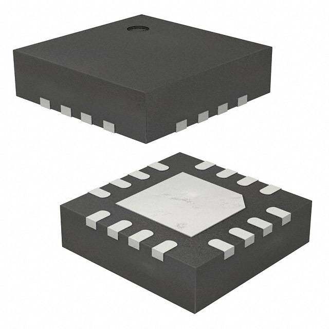
| 描述 | IC GAAS MESFET SW SPDT 16QFN |
| 产品分类 | |
| IIP3 | - |
| 品牌 | Hittite Microwave Corporation |
| 数据手册 | |
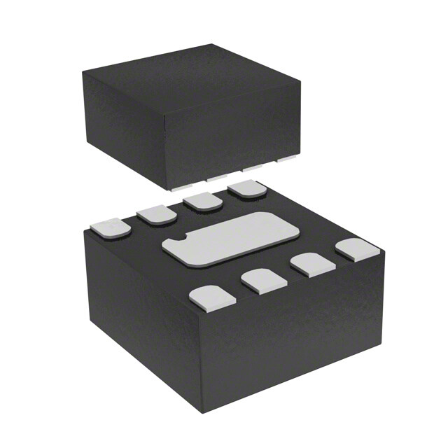
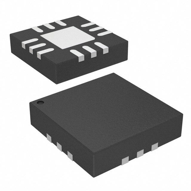
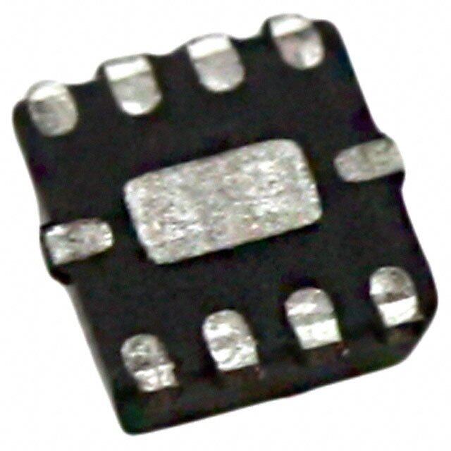
| 产品图片 |
|
| P1dB | 34dBm |
| 产品型号 | HMC349ALP4CE |
| RF类型 | 通用 |
| rohs | 无铅 / 符合限制有害物质指令(RoHS)规范要求 |
| 产品系列 | - |
| 供应商器件封装 | 16-QFN(4x4) |
| 其它名称 | 1127-1836-6 |
| 包装 | Digi-Reel® |
| 封装/外壳 | 16-VQFN 裸露焊盘 |
| 工作温度 | -40°C ~ 85°C |
| 拓扑 | 吸收性 |
| 插损@频率 | 1.4dB @ 4GHz |
| 标准包装 | 1 |
| 特性 | - |
| 特色产品 | http://www.digikey.cn/product-highlights/zh/new-hmc-series-spdt-switches/53047 |
| 电压-电源 | 4.5 V ~ 5.5 V |
| 电路 | SPDT |
| 配用 | /product-detail/zh/EV1HMC349ALP4C/1127-2780-ND/4863554 |
| 阻抗 | 50 欧姆 |
| 隔离@频率 | 62dB @ 4GHz (标准) |
| 频率 -上 | 4GHz |
| 频率 -下 | DC |


- 商务部:美国ITC正式对集成电路等产品启动337调查
- 曝三星4nm工艺存在良率问题 高通将骁龙8 Gen1或转产台积电
- 太阳诱电将投资9.5亿元在常州建新厂生产MLCC 预计2023年完工
- 英特尔发布欧洲新工厂建设计划 深化IDM 2.0 战略
- 台积电先进制程称霸业界 有大客户加持明年业绩稳了
- 达到5530亿美元!SIA预计今年全球半导体销售额将创下新高
- 英特尔拟将自动驾驶子公司Mobileye上市 估值或超500亿美元
- 三星加码芯片和SET,合并消费电子和移动部门,撤换高东真等 CEO
- 三星电子宣布重大人事变动 还合并消费电子和移动部门
- 海关总署:前11个月进口集成电路产品价值2.52万亿元 增长14.8%


PDF Datasheet 数据手册内容提取
High Isolation, Nonreflective, GaAs, SPDT Switch, 100 MHz to 4 GHz Data Sheet HMC349ALP4CE FEATURES FUNCTIONAL BLOCK DIAGRAM Nonreflective, 50 Ω design RF2 High isolation: 62 dB to 2 GHz HMC349ALP4CE VDD Low insertion loss: 1.0 dB to 2 GHz High input linearity 50Ω ER EN 1 dB power compression (P1dB): 34 dBm (typical) RFC V Third-order intercept (IP3): 53 dBm (typical) DRI CTRL High power handling 50Ω GND 2363..55 ddBBmm ttherrmouingaht pedat pha, tVhD D = 5 V RF1 17266-001 Single, positive supply: 3 V to 5 V Figure 1. CMOS-/TTL-compatible control All off state control 16-lead, 4 mm × 4 mm LFCSP Pin-compatible with the HMC8038 APPLICATIONS Wireless infrastructure Mobile radios Test equipment GENERAL DESCRIPTION The HMC349ALP4CE is a gallium arsenide (GaAs), single-pole, The HMC349ALP4CE operates with a single, positive supply double throw (SPDT) switch, specified from 100 MHz to 4 GHz. voltage from 3 V to 5 V and provides a CMOS-/TTL-compatible control interface. The HMC349ALP4CE is well suited for wireless infrastructure applications by yielding high isolation of 62 dB, low insertion The HMC349ALP4CE comes in a 16-lead, 4 mm × 4 mm, loss of 1.0 dB, high input IP3 of 53 dBm, and high input P1dB RoHS compliant, lead frame chip scale package (LFCSP). of 34 dBm. Rev. B Document Feedback Information furnished by Analog Devices is believed to be accurate and reliable. However, no responsibility is assumed by Analog Devices for its use, nor for any infringements of patents or other One Technology Way, P.O. Box 9106, Norwood, MA 02062-9106, U.S.A. rights of third parties that may result from its use. Specifications subject to change without notice. No license is granted by implication or otherwise under any patent or patent rights of Analog Devices. Tel: 781.329.4700 ©2019 Analog Devices, Inc. All rights reserved. Trademarks and registered trademarks are the property of their respective owners. Technical Support www.analog.com
HMC349ALP4CE Data Sheet TABLE OF CONTENTS Features .............................................................................................. 1 Interface Schematics .....................................................................5 Applications ....................................................................................... 1 Typical Performance Characterics ..................................................6 Functional Block Diagram .............................................................. 1 Insertion Loss, Isolation, and Return Loss ................................6 General Description ......................................................................... 1 Input Power Compression and Input Third-Order Intercept Revision History ............................................................................... 2 (IP3) ................................................................................................8 Specifications ..................................................................................... 3 Theory of Operation ...................................................................... 10 Absolute Maximum Ratings ............................................................ 4 Applications Information .............................................................. 11 Thermal Resistance ...................................................................... 4 Evaluation Board ........................................................................ 11 Power Derating Curve ................................................................. 4 Outline Dimensions ....................................................................... 12 ESD Caution .................................................................................. 4 Ordering Guide .......................................................................... 12 Pin Configuration and Function Descriptions ............................. 5 REVISION HISTORY This Hittite Microwave Products data sheet has been reformatted to Added Figure 12 ................................................................................ 7 meet the styles and standards of Analog Devices, Inc. Changes to Figure 13 ......................................................................... 7 Added Input Power Compression and Third-Order Intercept 1/2019—v02.0315 to Rev. B Section ................................................................................................. 8 Updated Format .................................................................. Universal Changes to Figure 14, Figure 15, and Figure 16 ............................ 8 Changes to Product Title, Features Section, Applications Added Figure 17, Figure 18, and Figure 19 .................................... 8 Section, General Description Section, and Figure 1 .................... 1 Added Figure 20, Figure 21, Figure 22, and Figure 23 ................. 9 Changes to Table 1 ............................................................................ 3 Added Theory of Operation Section ........................................... 10 Deleted Bias Voltage Table and Control Voltage Table ................ 3 Changes to Table 5 .......................................................................... 10 Changes to Table 2 ............................................................................ 4 Added Applications Information Section ................................... 11 Added Thermal Resistance Section, Power Derating Section, Changes to Evaluation Board Section, Figure 24, and and Figure 2 ....................................................................................... 4 Table 6 .............................................................................................. 11 Added Figure 3 .................................................................................. 5 Added Figure 25 ............................................................................. 11 Changes to Table 4 ............................................................................ 5 Updated Outline Dimensions ....................................................... 12 Added Interface Schematics Section .............................................. 5 Changes to Ordering Guide .......................................................... 12 Added Insertion Loss, Isolation, and Return Loss Section ......... 6 Changes to Figure 6, Figure 7, and Figure 8.................................. 6 Added Figure 9, Figure 10, and Figure 11 ..................................... 6 Rev. B | Page 2 of 12
Data Sheet HMC349ALP4CE SPECIFICATIONS Supply voltage (V ) = 3 V to 5 V, control voltage (V ) = 0 V or V , enable voltage (V ) = 0 V, case temperature (T ) = 25°C, DD CTRL DD EN CASE 50 Ω system, unless otherwise noted. Table 1. Parameter Symbol Test Conditions/Comments Min Typ Max Unit FREQUENCY RANGE 0.1 4 GHz INSERTION LOSS Between RFC and RF1/RF2 0.1 GHz to 1 GHz 0.9 1.2 dB 0.1 GHz to 2 GHz 1.0 1.3 dB 0.1 GHz to 3 GHz 1.1 1.5 dB 0.1 GHz to 4 GHz 1.2 1.7 dB ISOLATION Between RFC and RF1/RF2 0.1 GHz to 1 GHz 60 65 dB 0.1 GHz to 2 GHz 55 62 dB 0.1 GHz to 3 GHz 50 57 dB 0.1 GHz to 4 GHz 50 57 dB Between RF1 and RF2 0.1 GHz to 1 GHz 57 dB 0.1 GHz to 2 GHz 53 dB 0.1 GHz to 3 GHz 49 dB 0.1 GHz to 4 GHz 46 dB RETURN LOSS RFC 0.1 GHz to 1 GHz 21 dB 0.1 GHz to 2 GHz 21 dB 0.1 GHz to 3 GHz 17 dB 0.1 GHz to 4 GHz 15 dB RF1/RF2 On 0.1 GHz to 1 GHz 21 dB 0.1 GHz to 2 GHz 21 dB 0.1 GHz to 3 GHz 19 dB 0.1 GHz to 4 GHz 19 dB Off 0.5 GHz to 1 GHz 20 dB 0.5 GHz to 2 GHz 20 dB 0.5 GHz to 3 GHz 17 dB 0.5 GHz to 4 GHz 15 dB SWITCHING Rise and Fall Time t , t 10% to 90% of radio frequency (RF) output 60 ns RISE FALL On and Off Time t , t 50% V to 90% of RF output 150 ns ON OFF CTRL INPUT LINEARITY1 300 MHz to 4 GHz Input 0.1 dB Power Compression P0.1dB V = 3 V 25 dBm DD V = 5 V 31 dBm DD Input 1 dB Power Compression P1dB V = 3 V 28 dBm DD V = 5 V 30 34 dBm DD Input Third-Order Intercept IP3 Input power = 10 dBm/tone, Δf = 1 MHz V = 3 V 52 dBm DD V = 5 V 53 dBm DD SUPPLY INPUT VDD pin Voltage V 3 5 V DD Current I 1 3.5 mA DD DIGITAL INPUTS CTRL, EN pins Low Voltage V 0 0.8 V INL High Voltage V 2 V V INH DD Low Current I <1 µA INL High Current I 35 µA INH 1 For input linearity performance over frequency, see Figure 14 to Figure 23. Rev. B | Page 3 of 12
HMC349ALP4CE Data Sheet ABSOLUTE MAXIMUM RATINGS THERMAL RESISTANCE Table 2. Parameter Rating Thermal performance is directly linked to printed circuit Supply Voltage 7 V board (PCB) design and operating environment. Careful Digital Control Inputs attention to PCB thermal design is required. Voltage −1 V to V + 1 V DD θ is the junction to case bottom (channel to package bottom) JC Current 3 mA thermal resistance. RF Input Power1, 2, 3 (f = 300 MHz to 4 GHz, TCASE = 85°C) Table 3. Thermal Resistance Through Path Package Type θ Unit JC VDD = 3 V 31.5 dBm CP-16-40 VDD = 5 V 33.5 dBm Through Path 67.1 °C/W Terminated Path Terminated Path 144.2 °C/W V = 3 V to 5 V 26.5 dBm DD POWER DERATING CURVE Hot Switching 4 VDD = 3 V to 5 V 30 dBm TCASE = +85°C Temperature 0 TCASE = +125°C Junction (T) 150°C J –4 Storage −65°C to +150°C B) Reflow 260°C G (d –8 N Electrostatic Discharge (ESD) Sensitivity ATI–12 R Human Body Model (HBM) DE–16 R All Pins 250 V (Class 1A) E W–20 Supply Pin 350 V O P –24 1 For power derating at frequencies less than 300 MHz, see Figure 2. 2 In all off state, the RFC input power handling degrades by 6 dB from through –28 path specification. 3 Whinaphnuedntl i pnthogew d seeurg phrpaaldnyde aslni nbdgy c d6o edngBtrr aofrdlo vemos l bttahyg r6oe uds gBah rfe rpo namotht t pespromewcienifraiectdae tduio ppn,a RtahFn Cds p iRneFpc1iuf/itRc paFto2i wone.r –32 10k 100k F R1MEQUENCY 1(H0Mz) 100M 1G 17266-002 Figure 2. RF Input Power Derating Stresses at or above those listed under Absolute Maximum ESD CAUTION Ratings may cause permanent damage to the product. This is a stress rating only; functional operation of the product at these or any other conditions above those indicated in the operational section of this specification is not implied. Operation beyond the maximum operating conditions for extended periods may affect product reliability. Only one absolute maximum rating can be applied at any one time. Rev. B | Page 4 of 12
Data Sheet HMC349ALP4CE PIN CONFIGURATION AND FUNCTION DESCRIPTIONS C C C C NI NI NI NI 6 5 4 3 1 1 1 1 VDD 1 12 RF2 CTRL 2 HMC349ALP4CE 11 GND RFC 3 TOP VIEW 10 GND NIC 4 9 RF1 5 6 7 8 N C C C E NI NI NI NOTES 1.NIC = NOT INTERNALLY CONNECTED. 2 . EOBXEFP CTOHOSENE NPDECPCBAT.DE.D TTHOE TEHXEP ORSFE/DDCP GARDO MUUNSDT 17266-003 Figure 3. Pin Configuration Table 4. Pin Function Descriptions Pin No. Mnemonic Description 1 VDD Supply Voltage. 2 CTRL Logic Control Input. See Table 5. 3 RFC RF Common Port. This pin is dc-coupled and matched to 50 Ω. An external dc blocking capacitor is required on this pin. 4, 6 to 8, 13 to 16 NIC Not Internally Connected. These pins are not connected internally. 5 EN Logic Enable Input. See Table 5. 9 RF1 RF Throw Port 1. This pin is dc-coupled and matched to 50 Ω. An external dc blocking capacitor is required on this pin. 10, 11 GND Ground. These pins must be connected to the RF/dc ground of the PCB. 12 RF2 RF Throw Port 2. This pin is dc-coupled and matched to 50 Ω. An external dc blocking capacitor is required on this pin. EPAD Exposed Pad. The exposed pad must be connected to the RF and dc ground of the PCB. INTERFACE SCHEMATICS VDD RFC, RRFF12, 17266-004 CTRL, EN 500Ω 17266-005 Figure 4. RFC, RF1, and RF2 Interface Schematic Figure 5. Digital Pins (CTRL and EN) Interface Schematic Rev. B | Page 5 of 12
HMC349ALP4CE Data Sheet TYPICAL PERFORMANCE CHARACTERICS INSERTION LOSS, ISOLATION, AND RETURN LOSS V = 5 V, V = 0 V or V , V = 0 V or V , and T = 25°C, 50 Ω system, unless otherwise noted. Measured on the evaluation board. DD CTRL DD EN DD CASE The board loss is subtracted for insertion loss and isolation. However, return loss includes the board effects. 0 0 TCASE = +85°C TCASE = +85°C TCASE = +25°C TCASE = +25°C TCASE = –40°C TCASE = –40°C –0.5 –0.5 B) B) S (d–1.0 S (d–1.0 S S O O N L–1.5 N L–1.5 O O RTI RTI E E NS–2.0 NS–2.0 I I –2.5 –2.5 –3.00 0.5 1.0 1.5 FR2.E0QUE2N.5CY (3G.0Hz)3.5 4.0 4.5 5.0 17266-006 –3.00 0.5 1.0 1.5 FR2E.0QUE2N.5CY (G3.H0z) 3.5 4.0 4.5 5.0 17266-009 Figure 6. Insertion Loss Between RFC and RF1 vs. Frequency Figure 9. Insertion Loss Between RFC and RF2 vs. Frequency over Temperature over Temperature 0 0 –10 TTTCCCAAASSSEEE === ++–482055°°°CCC –10 TTTCCCAAASSSEEE === ++–482055°°°CCC –20 –20 –30 –30 B) B) N (d–40 N (d–40 O O ATI–50 ATI–50 L L O–60 O–60 S S I I –70 –70 –80 –80 –90 –90 –1000 0.5 1.0 1.5 FR2.E0QUE2N.5CY (3G.0Hz)3.5 4.0 4.5 5.0 17266-007 –1000 0.5 1.0 1.5 FR2E.0QUE2N.5CY (G3.H0z) 3.5 4.0 4.5 5.0 17266-010 Figure 7. Isolation Between RFC and RF1 vs. Frequency Figure 10. Isolation Between RFC and RF2 vs. Frequency over Temperature over Temperature 0 0 –10 TTTCCCAAASSSEEE === ++–482055°°°CCC –10 RRRFFFCC1TTTOOO RRRFFF212 –20 –20 –30 –30 ISOLATION (dB)–––654000 ISOLATION (dB)–––654000 –70 –70 –80 –80 –90 –90 –1000 0.5 1.0 1.5 FR2.E0QUE2N.5CY (3G.0Hz)3.5 4.0 4.5 5.0 17266-008 –1000 0.5 1.0 1.5 FR2E.0QUE2N.5CY (3G.0Hz) 3.5 4.0 4.5 5.0 17266-011 Figure 8. Isolation Between RF1 and RF2 vs. Frequency Figure 11. Isolation Between All RF Pins vs. Frequency over Temperature in All Off State (EN = VDD) Rev. B | Page 6 of 12
Data Sheet HMC349ALP4CE 0 0 TCASE = +85°C ON TCASE = +25°C OFF TCASE = –40°C –5 –5 B)–10 B)–10 d d S ( S ( S S O O L–15 L–15 N N R R U U T T RE–20 RE–20 –25 –25 –300 0.5 1.0 1.5 FR2E.0QUE2N.5CY (G3.H0z) 3.5 4.0 4.5 5.0 17266-012 –300 0.5 1.0 1.5 FR2.E0QUE2N.5CY (3G.0Hz)3.5 4.0 4.5 5.0 17266-013 Figure 12. Return Loss for RFC vs. Frequency over Temperature Figure 13. Return Loss for RF1 and RF2 vs. Frequency Rev. B | Page 7 of 12
HMC349ALP4CE Data Sheet INPUT POWER COMPRESSION AND INPUT THIRD-ORDER INTERCEPT (IP3) V = 3 V or 5 V, V = 0 V or V , V = V , and T = 25°C, 50 Ω system, unless otherwise noted. Measured on the evaluation board. DD CTRL DD EN DD CASE 36 36 34 TTTCCCAAASSSEEE === ++–482055°°°CCC 34 TTTCCCAAASSSEEE === ++–482055°°°CCC 32 32 m) 30 m) 30 B B B (d 28 B (d 28 d d 1 26 1 26 0. 0. P P T 24 T 24 U U P P IN 22 IN 22 20 20 18 18 160 0.5 1.0 1.5 FR2.E0QUE2N.5CY (3G.0Hz)3.5 4.0 4.5 5.0 17266-014 160 0.5 1.0 1.5 FR2E.0QUE2N.5CY (G3.H0z) 3.5 4.0 4.5 5.0 17266-017 Figure 14. Input 0.1 dB Power Compression (P0.1dB) vs. Frequency Figure 17. Input P0.1dB vs. Frequency over Temperature, VDD = 3 V over Temperature, VDD = 5 V 36 36 TCASE = +85°C 34 34 TTCCAASSEE == +–4205°°CC 32 32 30 30 m) m) dB 28 dB 28 B ( B ( 1d 26 1d 26 P P UT 24 UT 24 P P N N I 22 I 22 20 20 TCASE = +85°C 18 TCASE = +25°C 18 TCASE = –40°C 160 0.5 1.0 1.5 FR2.E0QUE2N.5CY (3G.0Hz)3.5 4.0 4.5 5.0 17266-015 160 0.5 1.0 1.5 FR2.E0QUE2N.5CY (3G.0Hz)3.5 4.0 4.5 5.0 17266-018 Figure 15. Input 1 dB Power Compression (P1dB) vs. Frequency Figure 18. Input P1dB vs. Frequency over Temperature, VDD = 3 V over Temperature, VDD = 5 V 60 60 55 55 50 50 45 45 m) m) B 40 B 40 d d P3 ( 35 P3 ( 35 T I T I PU 30 PU 30 N N I I 25 25 20 20 TCASE = +85°C TCASE = +85°C 15 TCASE = +25°C 15 TCASE = +25°C TCASE = –40°C TCASE = –40°C 100 0.5 1.0 1.5 FR2E.0QUE2N.5CY (3G.0Hz) 3.5 4.0 4.5 5.0 17266-016 100 0.5 1.0 1.5 FR2.E0QUE2N.5CY (3G.0Hz)3.5 4.0 4.5 5.0 17266-019 Figure 16. Input IP3 vs. Frequency over Temperature, VDD = 5 V Figure 19. Input IP3 vs. Frequency over Temperature, VDD = 3 V Rev. B | Page 8 of 12
Data Sheet HMC349ALP4CE 40 40 INPUT P0.1dB INPUT P0.1dB INPUT P1dB INPUT P1dB m) 35 m) 35 B B d d N ( 30 N ( 30 O O SI SI S 25 S 25 E E R R P P M 20 M 20 O O C C R R E 15 E 15 W W O O T P 10 T P 10 U U P P N N I 5 I 5 010k 100k F1RMEQUENCY1 (0HMz) 100M 1G 17266-020 010k 100k F1RMEQUENCY1 (0HMz) 100M 1G 17266-022 Figure 20. Input P0.1dB and Input P1dB vs. Frequency over Temperature, Figure 22. Input P0.1dB and Input P1dB vs. Frequency over Temperature, VDD = 5 V, Low Frequency Detail VDD = 3 V, Low Frequency Detail 60 60 55 55 50 50 45 45 m) m) B 40 B 40 d d P3 ( 35 P3 ( 35 T I T I PU 30 PU 30 N N I I 25 25 20 20 15 15 1010k 100k F1RMEQUENCY1 (0HMz) 100M 1G 17266-021 10 10k 100k F R1EMQUENCY (1H0zM) 100M 1G 17266-023 Figure 21. Input IP3 vs. Frequency over Temperature, VDD = 5 V, Figure 23. Input IP3 vs. Frequency over Temperature, VDD = 3 V, Low Frequency Detail Low Frequency Detail Rev. B | Page 9 of 12
HMC349ALP4CE Data Sheet THEORY OF OPERATION The HMC349ALP4CE requires a positive supply voltage applied to When the EN pin is logic high, the switch is in the all off state, the VDD pin. Bypassing capacitors are recommended on the and both RF paths are in the isolation state regardless of the supply lines to minimize RF coupling. logic level applied to the CTRL. In the all off state, the RF1 and RF2 ports are terminated to internal 50 Ω resistors, and RFC The HMC349ALP4CE is internally matched to 50 Ω at the RF becomes open reflective. common port (RFC) and the RF throw ports (RF1 and RF2). Therefore, no external matching components are required. All The switch design is bidirectional. The through path has same RF ports are dc-coupled, and dc blocking capacitors are power handling whether the RF input signal is applied to the required at the RF ports. RFC port or the selected RF throw port. An RF signal can also be applied to the terminated path that has lower power handling The HMC349ALP4CE incorporates a driver to perform logic than the through path (see Table 2). functions internally and to provide the user with the advantage of a simplified control interface. The driver features two digital The ideal power-up sequence is as follows: control input pins, CTRL and EN, which control the state of the 1. VDD. RF paths. 2. CTRL and EN (the relative order is not important). When the EN pin is logic low, the logic level applied to the 3. RF input signal. CTRL pin determines which RF path is in the insertion loss The ideal power-down sequence is the reverse order of the state while the other path is in the isolation state. The insertion power-up sequence. loss path conducts the RF signal between the selected RF throw port and the RF common port. The isolation path provides high loss between the insertion loss path and the unselected RF throw port that is terminated to an internal 50 Ω resistor. Table 5. Control Voltage Truth Table Digital Control Input RF Paths EN CTRL RF1 to RFC RF2 to RFC Low Low Isolation (off) Insertion loss (on) Low High Insertion loss (on) Isolation (off) High Low Isolation (off) Isolation (off) High High Isolation (off) Isolation (off) Rev. B | Page 10 of 12
Data Sheet HMC349ALP4CE APPLICATIONS INFORMATION EVALUATION BOARD Figure 25 and Table 6 are the evaluation board schematic and bill of materials, respectively. The HMC349ALP4CE uses a 4-layer evaluation board. The copper thickness is 0.5 oz (0.7 mil) on each layer. The top J5 J6 GND dielectric material is 10 mil Rogers RO4350, which offers good D VD C4 GND high frequency performance, and the middle and bottom 100pF J7 dielectric materials are FR-4 type materials to achieve an overall board thickness of 62 mil. All RF and dc traces are routed on the top copper layer and the inner and bottom layers are J4 61 51 41 31 C2 grounded planes that provide a solid ground for the RF TRL 1 VDDNIC NIC NIC NICRF2 12 100pF RF2J2 C transmission lines. The RF transmission lines are designed C1 2 CTRL GND 11 J1 100pF HMC349ALP4CE using a coplanar waveguide (CPWG) model with a width of RFC 3 10 RFC GND C3 13 mil and ground spacing of 10 mil for a characteristic 4 9 100pF RF1J3 NIC RF1 impedance of 50 Ω. For good RF and thermal grounding, as EN NIC NIC NIC many plated through vias as possible are arranged around 5 6 7 8 transmission lines and under the exposed pad of the package. EN Figure 24 shows the top view of the populated J8 EV1HMC349ALP4CE evaluation board. The package ground pins are connected directly to the ground plane which C5 C6 issu cpopnlyn pecotretd i st oc othnen eGcNteDd tdoc t phien ds c( Jp6i na nladb Je7le).d A V sDinDg l(eJ 5p)o. wAenr DEJP9OP DEPOP THRU DEPOP DEJP10OP 17266-025 Figure 25. Evaluation Board Schematic unpopulated bypass capacitor position is available to filter high frequency noise on the supply trace. Two control ports Table 6. Bill of Materials, Evaluation Board Components are connected to the CTRL and EN dc pins (J4 and J8). The Component Description RF ports are connected to the RFC, RF1, and RF2 connectors J1 to J3 PC mount SMA connectors (J1, J3, and J2) that are PC mount subminiature version J4 to J8 DC pins A (SMA) RF connectors. Additionally, 100 pF dc blocking J9, J10 PC mount SMA connectors, do not install (DNI) capacitors (C1, C2, and C3) are used on RF transmission lines. C1 to C4 Capacitors, 0402 package, 100 pF A through transmission line that connects unpopulated RF C5, C6 Capacitors, 0402 package, DNI connectors (J4 and J5) is also available to measure and remove U1 HMC349ALP4CE SPDT switch the loss of the PCB. PCB 106965-3 evaluation PCB 17266-024 Figure 24. Populated Evaluation Board Rev. B | Page 11 of 12
HMC349ALP4CE Data Sheet OUTLINE DIMENSIONS DETAIL A (JEDEC 95) 4.10 0.39 4.00 SQ 0.33 PIN 1 INDICATOR 3.90 0.27 AREA PININD I1CATORAREAOPTIONS 13 16 (SEEDETAILA) 0.65 1 BSC 12 2.55 EXPOSED 2.40 SQ PAD 2.25 9 4 *0.70 8 5 0.20 MIN TOP VIEW 0.60 BOTTOM VIEW 0.50 1.95 REF 1.00 FOR PROPER CONNECTION OF 0.90 SIDE VIEW 0.05 MAX THE EXPOSEDPAD,REFERTO 0.80 THEPINCONFIGURATION AND 0.02 NOM FUNCTION DESCRIPTIONS COPLANARITY SECTIONOFTHIS DATASHEET. SEATING 0.08 PLANE 0.20 REF PKG-005176 *CWOITMHP LEIXACNETP TTOIO JNE TDOE CL ESATDA NLDEANRGDTSH MO-220-VGGC-4 08-29-2018-A Figure 26. 16-Lead Lead Frame Chip Scale Package [LFCSP] 4 mm × 4 mm Body and 0.90 mm Package Height (CP-16-40) Dimensions shown in millimeters ORDERING GUIDE Model1 Temperature Range Package Description Package Option HMC349ALP4CE −40°C to +85°C 16-Lead Lead Frame Chip Scale Package [LFCSP] CP-16-40 HMC349ALP4CETR −40°C to +85°C 16-Lead Lead Frame Chip Scale Package [LFCSP] CP-16-40 EV1HMC349ALP4C Evaluation Board 1 The HMC349ALP4CE, the HMC349ALP4CETR, and the EV1HMC349ALP4C are RoHS compliant parts. ©2019 Analog Devices, Inc. All rights reserved. Trademarks and registered trademarks are the property of their respective owners. D17266-0-1/19(B) Rev. B | Page 12 of 12