ICGOO在线商城 > 射频/IF 和 RFID > RF 检测器 > HMC1020LP4E
 Datasheet下载
- 型号: HMC1020LP4E
- 制造商: Hittite
- 库位|库存: xxxx|xxxx
- 要求:
| 数量阶梯 | 香港交货 | 国内含税 |
| +xxxx | $xxxx | ¥xxxx |
查看当月历史价格
查看今年历史价格
HMC1020LP4E产品简介:
ICGOO电子元器件商城为您提供HMC1020LP4E由Hittite设计生产,在icgoo商城现货销售,并且可以通过原厂、代理商等渠道进行代购。 HMC1020LP4E价格参考¥54.58-¥56.10。HittiteHMC1020LP4E封装/规格:RF 检测器, RF Detector IC General Purpose 0Hz ~ 3.9GHz -65dBm ~ 7dBm ±1dB 24-VFQFN Exposed Pad。您可以下载HMC1020LP4E参考资料、Datasheet数据手册功能说明书,资料中有HMC1020LP4E 详细功能的应用电路图电压和使用方法及教程。
HMC1020LP4E是由Analog Devices Inc.(ADI公司)生产的一款RF检测器,广泛应用于射频(RF)和微波通信系统中。以下是该型号的主要应用场景:

 1. 功率测量与控制
HMC1020LP4E可以用于精确测量射频信号的功率电平。它能够将输入的RF信号转换为直流电压输出,该电压与输入信号的功率成正比。因此,它在需要实时监测和控制发射机输出功率的场景中非常有用,例如:
- 无线基站:确保基站发射的功率在规定范围内,避免过载或欠功率。
- 雷达系统:精确控制发射机的功率输出,以优化探测距离和精度。

 2. 自动增益控制(AGC)
在接收机中,HMC1020LP4E可以用于实现自动增益控制功能。通过检测接收到的信号强度,并根据信号强度调整放大器的增益,确保接收信号始终保持在最佳水平。这有助于提高系统的动态范围和抗干扰能力,适用于:
- 卫星通信:稳定接收链路中的信号强度,确保数据传输的可靠性。
- 无线电接收设备:保持接收信号的稳定性,特别是在信号强度波动较大的环境中。

 3. 频率合成器和锁相环(PLL)
HMC1020LP4E还可以用于频率合成器和锁相环电路中,作为参考信号的功率检测元件。通过检测反馈信号的功率,确保频率合成器的输出频率稳定且准确。这在需要高精度频率控制的应用中非常重要,如:
- 无线通信设备:确保发射和接收频率的准确性,避免频率漂移。
- 测试与测量仪器:提供稳定的频率参考,确保测量结果的准确性。

 4. 射频识别(RFID)系统
在RFID读写器中,HMC1020LP4E可以用于检测标签返回的信号强度,从而判断标签是否在有效范围内。这对于优化读写器的工作性能和提高识别率非常有帮助。

 5. 其他应用
此外,HMC1020LP4E还适用于各种需要精确RF功率检测的场合,如:
- 医疗设备:如超声波设备中的功率控制。
- 工业自动化:用于监控和控制射频加热设备的功率输出。

总之,HMC1020LP4E凭借其高精度、宽动态范围和低功耗等特点,成为射频通信、雷达、测试测量等领域中不可或缺的关键组件。
| 参数 | 数值 |
| 产品目录 | |
| 描述 | IC RMS PWR DETECTOR 65DB 24QFN |
| 产品分类 | |
| 品牌 | Hittite Microwave Corporation |
| 数据手册 | |
| 产品图片 |
|
| 产品型号 | HMC1020LP4E |
| RF类型 | 通用 |
| rohs | 无铅 / 符合限制有害物质指令(RoHS)规范要求 |
| 产品系列 | - |
| 其它名称 | 1127-1000-1 |
| 包装 | 剪切带 (CT) |
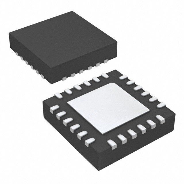
| 封装/外壳 | 24-VQFN 裸露焊盘 |
| 标准包装 | 1 |
| 特色产品 | http://www.digikey.cn/product-highlights/cn/zh/hittite-hmc102xlp4e-rms-detectors/2230 |
| 电压-电源 | 4.5 V ~ 5.5 V |
| 电流-电源 | 58mA |
| 精度 | ±1dB |
| 输入范围 | -65dBm ~ 7dBm |
| 频率 | 0Hz ~ 3.9GHz |


- 商务部:美国ITC正式对集成电路等产品启动337调查
- 曝三星4nm工艺存在良率问题 高通将骁龙8 Gen1或转产台积电
- 太阳诱电将投资9.5亿元在常州建新厂生产MLCC 预计2023年完工
- 英特尔发布欧洲新工厂建设计划 深化IDM 2.0 战略
- 台积电先进制程称霸业界 有大客户加持明年业绩稳了
- 达到5530亿美元!SIA预计今年全球半导体销售额将创下新高
- 英特尔拟将自动驾驶子公司Mobileye上市 估值或超500亿美元
- 三星加码芯片和SET,合并消费电子和移动部门,撤换高东真等 CEO
- 三星电子宣布重大人事变动 还合并消费电子和移动部门
- 海关总署:前11个月进口集成电路产品价值2.52万亿元 增长14.8%


PDF Datasheet 数据手册内容提取
Analog Devices Welcomes Hittite Microwave Corporation NO CONTENT ON THE ATTACHED DOCUMENT HAS CHANGED www.analog.com www.hittite.com
THIS PAGE INTENTIONALLY LEFT BLANK
HMC1020LP4E v02.0511 RMS POWER DETECTOR SINGLE-ENDED, DC - 3.9 GHz Typical Applications Features Broadband single-ended rF Input the HMc1020LP4e is ideal for: ±1 dB Detection Accuracy to 3.9 GHz • Log –> Root-Mean-Square (RMS) Conversion Input Dynamic range: -65 dBm to +7 dBm • Tx/Rx Signal Strength Indication (TSSI/RSSI) rF signal wave shape & crest Factor Independent • RF Power Amplifier Efficiency Control Digitally Programmable Integration Bandwidth • Receiver Automatic Gain Control excellent temperature stability • Transmitter Power Control Power-Down Mode 11 24 Lead 4x4mm sMt Package: 16mm² t M Functional Diagram General Descriptions s the HMc1020LP4e Power Detector is designed for - rF power measurement and control applications for s frequencies up to 3.9 GHz. the detector provides r an accurate rMs representation of any broadband, o single-ended rF/IF input signal. the output is a tem- t perature compensated, monotonic representation of c real signal power, measured with an input sensing e range of 72 dB. t the HMc1020LP4e is ideally suited to those wide e bandwidth, wide dynamic range applications requir- D ing repeatable measurement of real signal power, r especially where rF/IF wave shape and/or crest factor e change with time. w the integration bandwidth of the HMc1020LP4e is o digitally programmable with the use of input pins P scI1-4 over a range of more than 3 decades. this allows the user to dynamically set the operation bandwidth and also permits the detection of different types of modulations on the same platform. HMc1020LP4e features an internal op-amp at the out- put stage, which provides for slope / intercept adjust- ments and enables controller application. Electrical Specifications I TA = +25 °C, Vcc = 5V, Sci4 = Sci1 = 0V, Sci3 = Sci2 = 5V, Unless Otherwise Noted Parameter typ. typ. typ. typ. typ. typ. typ. Units Dynamic Range (±1dB Error) [1] Input Frequency 100 900 1900 2200 2700 3500 3900 MHz Single Ended Input Configuration 72 72 71 70 66 58 53 dB Deviation vs Temperature: (Over full temperature range -40 °C to 85 °C). 1 dB Deviation is measured from reference, which is the same WCDMA input at 25 °C. [1] With WCDMA 4 Carrier (TMI1-64 DPCH) For price, delivery and to place orders: Hittite Microwave Corporation, 20 Alpha Road, Chelmsford, MA 01824 11 - 1 Phone: 978-250-3343 Fax: 978-250-3373 Order On-line at www.hittite.com Application Support: Phone: 978-250-3343 or apps@hittite.com
HMC1020LP4E v02.0511 RMS POWER DETECTOR SINGLE-ENDED, DC - 3.9 GHz Electrical Specifications II TA = +25 °C, Vcc = 5V, Sci4 = Sci1 = 0V, Sci3 = Sci2 = 5V, Unless Otherwise Noted Parameter typ. typ. typ. typ. typ. typ. typ. Units Input Frequency 100 900 1900 2200 2700 3500 3900 MHz Modulation Deviation (Output deviation from reference, which is measured with CW input at equivalent input signal power) WCDMA 4 Carrier (TM1-64 DPCH) at +25 °C 0.1 0.1 0.1 0.1 0.1 0.1 0.1 dB WCDMA 4 Carrier (TM1-64 DPCH) at +85 °C 0.1 0.1 0.1 0.1 0.1 0.1 0.1 dB WCDMA 4 Carrier (TM1-64 DPCH) at -40 °C 0.1 0.1 0.1 0.1 0.1 0.1 0.1 dB Logarithmic Slope and Intercept [1] Logarithmic slope 35.0 35.2 36.0 36.6 37.9 41.5 44.4 mV/dB Logarithmic Intercept -68.2 -67.9 -66.5 -65.6 -63.6 -58.7 -55.3 dBm 11 Max. Input Power at ±1dB error 7 7 7 7 5 2 0 dBm Min. Input Power at ±1dB error -65 -65 -64 -63 -61 -56 -53 dBm [1] With WCDMA 4 Carrier (TM1-64 DPCH) t M RMSOUT vs. Pin with Different RMSOUT Error vs. Pin with Different s Modulations @ 1900 MHz [1] Modulations @ 1900 MHz [1] - 3 4 s 3 CW 2.5 Ideal WCDMA 4 carriers r CW 2 WCDMA1 o WCDMA 4 carriers CDMA2000 2 WCDMA1 V) CDMA2000 B) 1 LTEDW t OUT (1.5 LTEDW OR (d 0 c S R e RM 1 ER -1 t -2 e 0.5 -3 D 0 -4 r -70 -60 -50 -40 -30 -20 -10 0 10 -70 -60 -50 -40 -30 -20 -10 0 10 e INPUT POWER (dBm) INPUT POWER (dBm) w o P [1] Data was taken at sci4=sci1=0V, sci3=sci2=5V, shortest integration time is for scI=0000, allowed longest integration time is for scI=1100 For price, delivery and to place orders: Hittite Microwave Corporation, 20 Alpha Road, Chelmsford, MA 01824 Phone: 978-250-3343 Fax: 978-250-3373 Order On-line at www.hittite.com 11 - 2 Application Support: Phone: 978-250-3343 or apps@hittite.com
HMC1020LP4E v02.0511 RMS POWER DETECTOR SINGLE-ENDED, DC - 3.9 GHz Electrical Specifications III T = +25 °C, Vcc = 5V, Sci4 = Sci1 = 0V, Sci3 = Sci2 = 5V, Unless Otherwise Noted A Parameter conditions Min typ. Max Units Single-Ended Input Configuration Input Network return Loss up to 3.9 GHz > 15 dB Input resistance between INP and INN Between pins 3 and 4 100 Ω Input Voltage range Ac coupled peak voltage at INP 0.85 V RMSOUT Output output Voltage range 0.13 to 2.7 V source/sink current compliance rMsoUt held at Vcc/2 8 / -0.55 mA Output Slew Rate (rise / fall) sci4=sci3=sci2=sci1=0V, cofs=1nF 24 / 1.9 106 V/s 11 VSET Input (Negative Feedback Terminal) For control applications with nominal Input Voltage range 0.13 to 2.7 V slope/intercept settings Input resistance 5 MΩ t SCI1-4 Inputs, ENX Logic Input (Power Down Control) M Input High Voltage 0.7xVcc V s Input Low Voltage 0.3xVcc V - Input High current 1 μA s Input Low current 1 μA r Input capacitance 0.5 pf o Power Supply t supply Voltage 4.5 5 5.5 V c supply current with no input power 55 mA e supply current with Pin = -20dBm 58 mA t standby Mode supply current 5 mA e D r e w o P For price, delivery and to place orders: Hittite Microwave Corporation, 20 Alpha Road, Chelmsford, MA 01824 11 - 3 Phone: 978-250-3343 Fax: 978-250-3373 Order On-line at www.hittite.com Application Support: Phone: 978-250-3343 or apps@hittite.com
HMC1020LP4E v02.0511 RMS POWER DETECTOR SINGLE-ENDED, DC - 3.9 GHz RMSOUT & Error vs. Pin @ 100 MHz [1][2] RMSOUT & Error vs. Pin @ 900 MHz [1][2] 3.2 4 3.2 4 2.8 3 2.8 3 ERR +25C ERR +25C ERR +85C ERR +85C 2.4 ERR -40C 2 2.4 ERR -40C 2 RMSOUT (V) 11..262 -011 ERROR (dB RMSOUT (V) 11..262 -011 ERROR (dB ) ) 0.8 Ideal -2 0.8 Ideal -2 LOGOUT +25C LOGOUT +25C 0.4 LLOOGGOOUUTT +-4805CC -3 0.4 LLOOGGOOUUTT +-4805CC -3 11 0 -4 0 -4 -70 -60 -50 -40 -30 -20 -10 0 10 -70 -60 -50 -40 -30 -20 -10 0 10 INPUT POWER (dBm) INPUT POWER (dBm) t M s RMSOUT & Error vs. Pin @ 1900 MHz [1][2] RMSOUT & Error vs. Pin @ 2200 MHz [1][2] - 3.2 4 3.2 4 s 2.8 ERR +25C 3 2.8 ERR +25C 3 r ERR +85C ERR +85C 2.4 ERR -40C 2 2.4 ERR -40C 2 o RMSOUT (V) 11..262 -011 ERROR (dB) RMSOUT (V) 11..262 -011 ERROR (dB) tect 0.8 Ideal -2 0.8 Ideal -2 e LOGOUT +25C LOGOUT +25C 0.4 LOGOUT +85C -3 0.4 LOGOUT +85C -3 D LOGOUT -40C LOGOUT -40C 0 -4 0 -4 r -70 -60 -50 -40 -30 -20 -10 0 10 -70 -60 -50 -40 -30 -20 -10 0 10 e INPUT POWER (dBm) INPUT POWER (dBm) w o P RMSOUT & Error vs. Pin @ 2700 MHz [1][2] RMSOUT & Error vs. Pin @ 3500 MHz [1][2] 3.2 4 3.2 4 2.8 ERR +25C 3 2.8 ERR +25C 3 ERR +85C ERR +85C 2.4 ERR -40C 2 2.4 ERR -40C 2 V) 2 1 E V) 2 1 E RMSOUT ( 11..26 -01 RROR (dB RMSOUT ( 11..26 -01 RROR (dB ) ) 0.8 Ideal -2 0.8 Ideal -2 LOGOUT +25C LOGOUT +25C 0.4 LOGOUT +85C -3 0.4 LOGOUT +85C -3 LOGOUT -40C LOGOUT -40C 0 -4 0 -4 -70 -60 -50 -40 -30 -20 -10 0 10 -70 -60 -50 -40 -30 -20 -10 0 10 INPUT POWER (dBm) INPUT POWER (dBm) [1] Data was taken at sci4=sci1=0V, sci3=sci2=5V, shortest integration time is for scI=0000, allowed longest integration time is for scI=1100 [2] wcDMA 4 carriers input waveform For price, delivery and to place orders: Hittite Microwave Corporation, 20 Alpha Road, Chelmsford, MA 01824 Phone: 978-250-3343 Fax: 978-250-3373 Order On-line at www.hittite.com 11 - 4 Application Support: Phone: 978-250-3343 or apps@hittite.com
HMC1020LP4E v02.0511 RMS POWER DETECTOR SINGLE-ENDED, DC - 3.9 GHz RMSOUT & Error vs. Pin @ 3900 MHz [1][2] Intercept vs. Frequency [1][2] 3.2 4 -50 2.8 ERR +25C 3 ERR +85C -55 2.4 ERR -40C 2 m) B-60 +25C RMSOUT (V) 11..262 -011 ERROR (dB) NTERCEPT (d--7605 + -8450CC 0.8 Ideal -2 I LOGOUT +25C -75 11 0.4 LOGOUT +85C -3 LOGOUT -40C 0 -4 -80 0 1000 2000 3000 4000 -70 -60 -50 -40 -30 -20 -10 0 10 FREQUENCY (MHz) INPUT POWER (dBm) t M RMSOUT vs. Pin with WCDMA s Slope vs. Frequency [1][2] 4 Carrier @ +25 °C [1] - 50 3 s 100MHz r 2.5 900MHz 1900MHz o 45 2200MHz ect OPE (mV/dB) 40 ++ -284550CCC MSOUT (V) 1.52 233759000000MMMHHHzzz t SL R 1 e 35 0.5 D r 30 0 0 1000 2000 3000 4000 -70 -60 -50 -40 -30 -20 -10 0 10 e FREQUENCY (MHz) INPUT POWER (dBm) w o RMSOUT Error vs. Pin with WCDMA 4 RMSOUT Error vs. Pin with WCDMA 4 P Carrier @ +25 °C [1] Carrier @ +85 °C wrt +25 °C Response [1] 4 4 3 3 100MHz 900MHz 1900MHz 2 2 2200MHz 2700MHz OR (dB) 01 OR (dB) 01 33590000MMHHzz R R ER -1 100MHz ER -1 900MHz -2 1900MHz -2 2200MHz 2700MHz -3 3500MHz -3 3900MHz -4 -4 -70 -60 -50 -40 -30 -20 -10 0 10 -70 -60 -50 -40 -30 -20 -10 0 10 INPUT POWER (dBm) INPUT POWER (dBm) [1] Data was taken at sci4=sci1=0V, sci3=sci2=5V, shortest integration time is for scI=0000, allowed longest integration time is for scI=1100 [2] wcDMA 4 carriers input waveform For price, delivery and to place orders: Hittite Microwave Corporation, 20 Alpha Road, Chelmsford, MA 01824 11 - 5 Phone: 978-250-3343 Fax: 978-250-3373 Order On-line at www.hittite.com Application Support: Phone: 978-250-3343 or apps@hittite.com
HMC1020LP4E v02.0511 RMS POWER DETECTOR SINGLE-ENDED, DC - 3.9 GHz RMSOUT Error vs. Pin with WCDMA 4 Carrier @ -40 °C wrt +25 °C Response [1] RMSOUT vs. Pin with CW @ +25 °C [1] 4 3 3 100MHz 100MHz 900MHz 2.5 900MHz 1900MHz 1900MHz 2 2200MHz 2200MHz OR (dB) 01 233759000000MMMHHHzzz OUT (V) 1.52 233759000000MMMHHHzzz R S R M E -1 R 1 -2 0.5 -3 11 -4 0 -70 -60 -50 -40 -30 -20 -10 0 10 -70 -60 -50 -40 -30 -20 -10 0 10 INPUT POWER (dBm) INPUT POWER (dBm) t M RMSOUT vs. Pin w/ CW & WCDMA 4 Carrier RMSOUT Error vs. Pin with CW @ +25 °C [1] @ 1900 MHz & +25 °C [1] s - 4 3 s 3 2.5 r 2 o B) 1 V) 2 CWWCDMA t OR (d 0 OUT ( 1.5 c RR MS e E -1 100MHz R 1 t 900MHz -2 1900MHz e 2700MHz -3 23250000MMHHzz 0.5 D 3900MHz -4 0 r -70 -60 -50 -40 -30 -20 -10 0 10 -70 -60 -50 -40 -30 -20 -10 0 10 INPUT POWER (dBm) INPUT POWER (dBm) e w o Reading Error for WCDMA 4 Carrier wrt RMSOUT vs. Pin w/ CW & WCDMA 4 Carrier P CW Response @ +25 °C [1] @ 1900 MHz & +85 °C [1] 1 3 0.8 0.6 2.5 0.4 OR (dB) 0.20 OUT (V) 1.52 CWWCDMA R S R-0.2 M E-0.4 190000MMHHzz R 1 1900MHz -0.6 2200MHz 2700MHz 0.5 -0.8 3500MHz 3900MHz -1 0 -70 -60 -50 -40 -30 -20 -10 0 10 -70 -60 -50 -40 -30 -20 -10 0 10 INPUT POWER (dBm) INPUT POWER (dBm) [1] Data was taken at sci4=sci1=0V, sci3=sci2=5V, shortest integration time is for scI=0000, allowed longest integration time is for scI=1100 For price, delivery and to place orders: Hittite Microwave Corporation, 20 Alpha Road, Chelmsford, MA 01824 Phone: 978-250-3343 Fax: 978-250-3373 Order On-line at www.hittite.com 11 - 6 Application Support: Phone: 978-250-3343 or apps@hittite.com
HMC1020LP4E v02.0511 RMS POWER DETECTOR SINGLE-ENDED, DC - 3.9 GHz Reading Error for WCDMA 4 Carrier wrt RMSOUT vs. Pin w/ CW & WCDMA 4 CW Response @ +85 °C [1] Carrier @ 1900 MHz & -40 °C [1] 1 3 0.8 2.5 0.6 OR (dB) 00..240 OUT (V) 1.52 CWWCDMA R S R-0.2 M E 100MHz R 1 -0.4 900MHz 1900MHz -0.6 2200MHz 2700MHz 0.5 11 -0.8 3500MHz 3900MHz -1 0 -70 -60 -50 -40 -30 -20 -10 0 10 -70 -60 -50 -40 -30 -20 -10 0 10 INPUT POWER (dBm) INPUT POWER (dBm) t M Reading Error for WCDMA 4 Carrier wrt Output Response s CW Response @ -40 °C [1] with SCI = 0000 @ 1900 MHz - 1 3 25 s 0.8 -20 dBm r 0.6 2.5 MSOUT 0 dBm 20 R o F etect ERROR (dB)---00000.....642240 191220092700000MM000MMMHHHHHzzzzz RMSOUT (V)01..5512 ORFFF ORNF ORFFF RF ENABLE 051105 ENABLE VOLTAGE (V D -0.8 3500MHz ) 3900MHz r -1 0 -5 -70 -60 -50 -40 -30 -20 -10 0 10 -2 0 2 4 6 8 10 e INPUT POWER (dBm) TIME (us) w o Output Response P with SCI = 1100 @ 1900 MHz Typical Supply Current vs. Pin, Vcc = 5V 3 25 70 -20 dBm 2.5 RMSOUT 0 dBm 20 65 R A) F m RMSOUT (V)1.512 51105 ENABLE VOLTA PLY CURRENT ( 556050 ++2855CC RF RF RF GE UP -40C 0.5 OFF ON OFF 0 (V) S 45 RF ENABLE 0 -5 40 -70 -60 -50 -40 -30 -20 -10 0 10 0 1 2 3 4 5 6 7 8 9 10 11 12 13 14 15 16 17 INPUT POWER (dBm) TIME (ms) [1] Data was taken at sci4=sci1=0V, sci3=sci2=5V, shortest integration time is for scI=0000, allowed longest integration time is for scI=1100 For price, delivery and to place orders: Hittite Microwave Corporation, 20 Alpha Road, Chelmsford, MA 01824 11 - 7 Phone: 978-250-3343 Fax: 978-250-3373 Order On-line at www.hittite.com Application Support: Phone: 978-250-3343 or apps@hittite.com
HMC1020LP4E v02.0511 RMS POWER DETECTOR SINGLE-ENDED, DC - 3.9 GHz Output Ripple & Rise/Fall Time vs. Integration Setting Input Return Loss vs. Frequency [Sci4,Sci3,Sci2,Sci1] in Decimal 0 1800 100000 Ripple with WCDMA1 RETURN LOSS (dB)----2211-50505 Output Ripple Peak-Peak (mV)11369250000000000 RRRiiippppppllleee wwwiiittthhh W88 TTCooDnnMee A((114k0HkHz zs espeepreartaiotino)nRF)aislle T Timimee 11111000000000Rise Time & Fall Time (us)0 11 0 0.1 -30 0 1 2 3 4 5 6 0 1 2 3 4 5 6 7 8 9 10 11 12 FREQUENCY (GHz) Integration Setting (in Decimal) t M s - s r o t c e t e D r e w o P For price, delivery and to place orders: Hittite Microwave Corporation, 20 Alpha Road, Chelmsford, MA 01824 Phone: 978-250-3343 Fax: 978-250-3373 Order On-line at www.hittite.com 11 - 8 Application Support: Phone: 978-250-3343 or apps@hittite.com
HMC1020LP4E v02.0511 RMS POWER DETECTOR SINGLE-ENDED, DC - 3.9 GHz Absolute Maximum Ratings Power Supply Voltage (Vcc) 5.6V single ended rF Input Power 10 dBm eLectrostAtIc seNsItIVe DeVIce single ended Input Voltage Vcc + 0.6V oBserVe HANDLING PrecAUtIoNs Junction temperature 125 °c Continuous Pdiss (T = 85°C) 1.39 w (Derate 32.45 mW/°c above 85°C) Thermal Resistance (R ) th 28.68 °c/w (junction to ground paddle) storage temperature -65 to +150 °c 11 operating temperature -40 to +85 °c ESD Sensitivity (HBM) class 1B Outline Drawing t M s - s r o t c e t e D r e w o P Notes: 1. LeADFrAMe MAterIAL: coPPer ALLoY 2. DIMeNsIoNs Are IN INcHes [MILLIMeters]. 3. LeAD sPAcING toLerANce Is NoN-cUMULAtIVe 4. PAD BUrr LeNGtH sHALL Be 0.15mm MAXIMUM. PAD BUrr HeIGHt sHALL Be 0.05mm MAXIMUM. 5. PAcKAGe wArP sHALL Not eXceeD 0.05mm. 6. ALL GroUND LeADs AND GroUND PADDLe MUst Be soLDereD to PcB rF GroUND. 7. reFer to HMc APPLIcAtIoN Note For sUGGesteD PcB LAND PAtterN. Package Information Part Number Package Body Material Lead Finish MsL rating Package Marking [1] HMc1020LP4e roHs-compliant Low stress Injection Molded Plastic 100% matte sn MsL1 [2] H1020 XXXX [1] 4-Digit lot number XXXX [2] Max peak reflow temperature of 260 °C For price, delivery and to place orders: Hittite Microwave Corporation, 20 Alpha Road, Chelmsford, MA 01824 11 - 9 Phone: 978-250-3343 Fax: 978-250-3373 Order On-line at www.hittite.com Application Support: Phone: 978-250-3343 or apps@hittite.com
HMC1020LP4E v02.0511 RMS POWER DETECTOR SINGLE-ENDED, DC - 3.9 GHz Pin Descriptions Pin Number Function Description Interface schematic Bias supply. connect supply voltage to these pins 1, 16, 21, 23 Vcc with appropriate filtering. 11 2, 5, 6, 8, Package bottom has an exposed metal paddle that 11 - 13, 22, 24 GND must be connected to rF/Dc ground. Package Base t M s - s r o t c 3 ,4 INP, INN rF input pins. e t e D r e w o P Disable pin. connect to GND for normal operation. 7 eNX Applying voltage V>0.8xVcc will initiate power saving mode. For price, delivery and to place orders: Hittite Microwave Corporation, 20 Alpha Road, Chelmsford, MA 01824 Phone: 978-250-3343 Fax: 978-250-3373 Order On-line at www.hittite.com 11 - 10 Application Support: Phone: 978-250-3343 or apps@hittite.com
HMC1020LP4E v02.0511 RMS POWER DETECTOR SINGLE-ENDED, DC - 3.9 GHz Pin Descriptions (Continued) Pin Number Function Description Interface schematic Input high pass filter capacitor. Connect a capacitor coFsA, 9, 10 between coFsA and coFsB to determine 3 dB coFsB point of input signal high-pass filter. 11 t M s 14 Vset set input point for controller mode. - s r o t c Logarithmic output that provides an indication of e 15 rMsoUt mean square input power. t e D r e w Digital input pins that control the internal integration time constant for mean square calculation. scI4 is o the most significant bit. Set V>0.2xVcc to disable. scI1, scI2, P 17, 18, 19, 20 scI3, scI4 shortest integration time is for scI=0000, allowed longest integration time is for SCI=1100 (1101, 1110 and 1111 SCI settings are forbidden states). Each step changes the integration time by 1 octave. For price, delivery and to place orders: Hittite Microwave Corporation, 20 Alpha Road, Chelmsford, MA 01824 11 - 11 Phone: 978-250-3343 Fax: 978-250-3373 Order On-line at www.hittite.com Application Support: Phone: 978-250-3343 or apps@hittite.com
HMC1020LP4E v02.0511 RMS POWER DETECTOR SINGLE-ENDED, DC - 3.9 GHz Evaluation PCB 11 t M s - s r o t c e t e D List of Materials for Evaluation PCB r e the circuit board used in the application should Item Description w use rF circuit design techniques. signal lines sho-uld J1, J2 sMA connector have 50 ohm impedance while the package ground o tP1 - tP9 Dc Pin leads and exposed paddle should be connected P c1, c10, c16 100 pF capacitor, 0402 Pkg. directly to the ground plane similar to that shown. A c2, c5, c11, c17 100 nF capacitor, 0402 Pkg. sufficient number of via holes should be used to con- c3, c4, c6 1000 pF capacitor, 0402 Pkg. nect the top and bottom ground planes. the evalua- r2, r12 - r15 10K ohm resistor, 0402 Pkg. tion circuit board shown is available from Hittite upon r3 - r5, r9, r10 0 ohm resistor, 0402 Pkg. request. r6, r7 4.7K ohm resistor, 0402 Pkg. Board is configured with wideband single-ended input HMc1020LP4e interface suitable for input signal frequencies above U1 rMs Power Detector 100 MHz. refer to wideband single-ended input inter- PcB [1] 128683-1 evaluation PcB face section in application information for operating [1] circuit Board Material: rogers 4350 or Arlon 25Fr with signals below 100 MHz. Evaluation Order Information Item content Part Number evaluation PcB HMc1020LP4e evaluation PcB eVAL01-HMc1020LP4e For price, delivery and to place orders: Hittite Microwave Corporation, 20 Alpha Road, Chelmsford, MA 01824 Phone: 978-250-3343 Fax: 978-250-3373 Order On-line at www.hittite.com 11 - 12 Application Support: Phone: 978-250-3343 or apps@hittite.com
HMC1020LP4E v02.0511 RMS POWER DETECTOR SINGLE-ENDED, DC - 3.9 GHz Application Circuit 11 t M s - s r o t c e t e D r e w o P For price, delivery and to place orders: Hittite Microwave Corporation, 20 Alpha Road, Chelmsford, MA 01824 11 - 13 Phone: 978-250-3343 Fax: 978-250-3373 Order On-line at www.hittite.com Application Support: Phone: 978-250-3343 or apps@hittite.com
HMC1020LP4E v02.0511 RMS POWER DETECTOR SINGLE-ENDED, DC - 3.9 GHz Application Information Principle of Operation 11 t M s - the HMc1020LP4e power detector is the optimal solution for monitoring and controlling transmitted and received s signal power, measuring the incident rF signal power, and then generating an output signal representing the input r power level. o t the HMc1020LP4e is a monolithic true-rMs detector, which in fact is an analog calculator, designed to measure c the actual rMs power of the input signal, independent of the modulated signal waveform complexity or modulation e scheme. At the core of an RMS detector is a full-wave rectifier, log/antilog circuit, and an integrator. The RMS output t signal is directly proportional to the logarithm of the time-average of V 2. the bias block also contains temperature IN e compensation circuits which stabilize output accuracy over the entire operating temperature range. the Dc offset D cancellation circuit actively cancels internal offsets so that even very small input signal levels can be measured r accurately. e the HMc1020LP4e achieves exceptional rF power measurement accuracy independent of the modulation of the w carrier, with the system architecture shown in the block diagram figure. The relation between the HMC1020LP4E’s o rMsoUt output and the rF input power is given below: P P = rMsoUt / [log-slope] + [log-intercept], dBm IN Configuration For The Typical Application the HMc1020LP4e is a logarithmic rMs detector that can be directly driven with a single-ended 50-ohm rF source. the integrated broadband single-ended input interface of HMc1020LP4e eliminates the requirement for an external balun transformer or a matching network. the HMc1020LP4e can be operated from Dc to 3.9 GHz by using only standard Dc blocking capacitors. this simple input interface provides cost and PcB area reductions and increases measurement repeatability. The RMS output signal is typically connected to VSET through a resistive network providing a Pin -> RMSOUT transfer characteristic slope of 35.2 mV/dB ( at 900 MHz). However the RMS output can be re-scaled to “magnify” a specific portion of the input sensing range, and to fully utilize the dynamic range of the RMS output. Refer to the section under the “log-slope and intercept” heading for details. For price, delivery and to place orders: Hittite Microwave Corporation, 20 Alpha Road, Chelmsford, MA 01824 Phone: 978-250-3343 Fax: 978-250-3373 Order On-line at www.hittite.com 11 - 14 Application Support: Phone: 978-250-3343 or apps@hittite.com
HMC1020LP4E v02.0511 RMS POWER DETECTOR SINGLE-ENDED, DC - 3.9 GHz Due to part-to-part variations in log-slope and log-intercept, a system-level calibration is recommended to satisfy absolute accuracy requirements; refer to the “System Calibration” section for more details. Broadband Single-Ended Input Interface the HMc1020LP4e operates with a single-ended input interface and requires only two external Dc blocking capacitors and an external 50 ohm resistor. the HMc1020LP4e input interface shown below provides a compact, broadband solution. 11 t M s - Note that the provided single-ended input interface covers the whole operating spectrum of the HMc1020LP4e s and does not require matching/tuning for different frequencies. the performance of the HMc1020LP4e at different r frequencies is shown below: o t c RMSOUT & Error vs. Pin e t 3.2 4 ERR 100MHz e 2.8 EERRRR 1990000MMHHzz 3 D ERR 2200MHz 2.4 EERRRR 23750000MMHHzz 2 ERR 3900MHz r V) 2 1 E we RMSOUT ( 11..26 -01 RROR (dB o LOGOUT 100MHz ) 0.8 LOGOUT 900MHz -2 P LOGOUT 1900MHz LOGOUT 2200MHz 0.4 LOGOUT 2700MHz -3 LOGOUT 3500MHz 0 LOGOUT 3900MHz -4 -70 -60 -50 -40 -30 -20 -10 0 10 INPUT POWER (dBm) For price, delivery and to place orders: Hittite Microwave Corporation, 20 Alpha Road, Chelmsford, MA 01824 11 - 15 Phone: 978-250-3343 Fax: 978-250-3373 Order On-line at www.hittite.com Application Support: Phone: 978-250-3343 or apps@hittite.com
HMC1020LP4E v02.0511 RMS POWER DETECTOR SINGLE-ENDED, DC - 3.9 GHz RMS Output Interface and Transient Response The HMC1020LP4E features digital input pins (SCI1-SCI4) that control the internal integration time constant. Output transient response is determined by the digital integration controls, and output load conditions. Shortest integration time is for SCI=0000, allowed longest integration time is for SCI=1100 (1101, 1110 and 1111 SCI settings are forbidden states). Using larger values of scI will narrow the operating bandwidth of the integrator, resulting in a longer averaging time interval and a more filtered output signal. It will also slow the power detector’s transient response. A larger scI value favors output accuracy over speed. For the fastest possible transient settling times set scI to 0000. this configuration will operate the integrator at its widest possible bandwidth, resulting in short averaging time-interval 11 and an output signal with little filtering. For most applications an SCI setting may be selected to maintain a balance between speed and accuracy. Furthermore, error performance over modulation bandwidth is dependent on the scI setting. For example, modulations with relatively low frequency components and high crest factors may require higher SCI (integration) settings. t Table 1: Transient Response vs. SCI Setting [1]: M s RMSOUT Rise-Time 10% -> 90% (µs) [3] RMSOUT Rise Settling Time (µs) [2] RMSOUT Fall-time 100% -> 10% (µs) [4] - scI4,3,2,1 PdinB =m 0 Pind B=m -20 Pind B=m -40 PdinB =m 0 Pind B=m -20 Pind B=m -40 PdinB =m 0 Pind B=m -20 Pind B=m -40 s r 0000 0.0686 0.044 0.053 0.509 0.504 0.257 0.969 0.975 1 o 0010 0.0684 0.05 0.093 0.54 0.524 0.6788 2.98 3.193 3.35 t 0100 0.076 0.066 0.878 1.956 1.872 2.82 13.5 14.18 14.978 c 0110 1.624 3.432 4.84 7.8 8.056 8.92 62.9 65.384 69.224 e 1000 8.6 15.32 23.4 35.52 37.28 40.92 294.64 304.52 317.32 t 1010 38.6 65.8 109.6 165.2 156 188 1379.4 1423.6 1477.6 e 1100 186 325 509 802 770 831 6447 6640 6881 D r e w o P [1] Input signal is 1900 MHz cw -tone switched on and off [2] Measured from RF switching edge to 1dB (input referred) settling of RMSOUT. [3] Measured from 10% to 90% [4] Measured from 100% to 10% For price, delivery and to place orders: Hittite Microwave Corporation, 20 Alpha Road, Chelmsford, MA 01824 Phone: 978-250-3343 Fax: 978-250-3373 Order On-line at www.hittite.com 11 - 16 Application Support: Phone: 978-250-3343 or apps@hittite.com
HMC1020LP4E v02.0511 RMS POWER DETECTOR SINGLE-ENDED, DC - 3.9 GHz Rise Time[1] vs. Rise Settling Time[2] vs. SCI Setting over Input Power SCI Setting over Input Power 10000 100000 -40 dBm -40 dBm 1000 -20 dBm 10000 -20 dBm 0 dBm 0 dBm s)100 s)1000 u u E ( E ( M M TI 10 TI100 E E S S RI 1 RI 10 11 0.1 1 0.01 0.1 0 1 2 3 4 5 6 7 8 9 10 11 12 0 1 2 3 4 5 6 7 8 9 10 11 12 INTEGRATION SETTING (IN DECIMAL) INTEGRATION SETTING (IN DECIMAL) t M Fall Time[1] vs. s SCI Setting over Input Power - 100000 For increased load drive capability, consider a buffer s amplifier on the RMS output. Using an integrating r -40 dBm amplifier on the RMS output allows for an alternative 10000 -20 dBm o 0 dBm treatment for faster settling times. An external t us) amplifier optimized for transient settling can also c ME (1000 provide additional RMS filtering, when operating TI e L HMc1020LP4e with a lower scI value. L100 t FA e Following figures show how the peak-to-peak ripple 10 D decreases with higher scI settings along with the rF pulse response over different modulations. r 1 0 1 2 3 4 5 6 7 8 9 10 11 12 e INTEGRATION SETTING (IN DECIMAL) w o Residual Ripple for 900 Mhz Residual Ripple for 900 Mhz P WiMAX @ SCI=0100 WiMAX @ SCI=0110 2 100 2 100 1.8 80 1.8 80 1.6 60 1.6 60 R R F F OUT (V)11..241 INRPFUT 02400 INPUT VO OUT (V)11..241 INRPFUT 02400 INPUT VO RMS0.8 -20 LTAG RMS0.8 -20 LTAG 0.6 -40 E 0.6 -40 E 0.4 RMSOUT SCI = 0000 -60 (mV) 0.4 RMSOUT SCI = 0000 -60 (mV) 0.2 SCI = 0100 -80 0.2 SCI = 0110 -80 0 -100 0 -100 0 50 100 150 200 250 300 350 400 450 500 0 50 100 150 200 250 300 350 400 450 500 TIME (us) TIME (us) [1] Measured from 10% to 90% [2] Measured from RF switching edge to 1dB (input referred) settling of RMSOUT. [3] Measured from 100% to 10% For price, delivery and to place orders: Hittite Microwave Corporation, 20 Alpha Road, Chelmsford, MA 01824 11 - 17 Phone: 978-250-3343 Fax: 978-250-3373 Order On-line at www.hittite.com Application Support: Phone: 978-250-3343 or apps@hittite.com
HMC1020LP4E v02.0511 RMS POWER DETECTOR SINGLE-ENDED, DC - 3.9 GHz Residual Ripple for 900 Mhz Residual Ripple for 900 Mhz WiBRO @ SCI=0100 WiBRO @ SCI=0110 2 100 2 100 1.8 80 1.8 80 1.6 60 1.6 60 R R F F OUT (V)11..241 INRPFUT 02400 INPUT VO OUT (V)11..241 INRPFUT 02400 INPUT VO RMS0.8 -20 LTAG RMS0.8 -20 LTAG 0.6 -40 E 0.6 -40 E 00..24 RMSOUT SSCCII == 00010000 --8600 (mV) 00..24 RMSOUT SSCCII == 00010100 --8600 (mV) 11 0 -100 0 -100 0 0.5 1 1.5 2 2.5 3 3.5 4 4.5 5 0 0.5 1 1.5 2 2.5 3 3.5 4 4.5 5 TIME (ms) TIME (ms) t M Residual Ripple for 900 Mhz Residual Ripple for 900 Mhz s LTE Downlink @ SCI=0100 LTE Downlink @ SCI=0110 - 2.2 2.2 s 2 2 r 1.8 1.8 1.6 1.6 o V) 1.4 V) 1.4 t UT ( 1.2 UT ( 1.2 c O O S 1 S 1 e M M R 0.8 R 0.8 t 0.6 0.6 e 0.4 SCI = 0000 0.4 SCI = 0000 D 0.2 SCI = 0100 0.2 SCI = 0110 0 0 r 0 0.1 0.2 0.3 0.4 0.5 0 0.1 0.2 0.3 0.4 0.5 e TIME (ms) TIME (ms) w o Residual Ripple for 900 Mhz Residual Ripple for 900 Mhz P WCDMA4 @ SCI=0011 WCDMA4 @ SCI=0100 2.2 2.2 2 2 1.8 1.8 1.6 1.6 V) 1.4 V) 1.4 UT ( 1.2 UT ( 1.2 O O S 1 S 1 M M R 0.8 R 0.8 0.6 0.6 0.4 0.4 SCI = 0000 SCI = 0000 0.2 SCI = 0011 0.2 SCI = 0100 0 0 0 50 100 150 200 250 300 350 400 450 0 50 100 150 200 250 300 350 400 450 TIME (us) TIME (us) For price, delivery and to place orders: Hittite Microwave Corporation, 20 Alpha Road, Chelmsford, MA 01824 Phone: 978-250-3343 Fax: 978-250-3373 Order On-line at www.hittite.com 11 - 18 Application Support: Phone: 978-250-3343 or apps@hittite.com
HMC1020LP4E v02.0511 RMS POWER DETECTOR SINGLE-ENDED, DC - 3.9 GHz LOG-Slope and Intercept The HMC1020LP4E provides for an adjustment of output scale with the use of an integrated operational amplifier. Logarithmic slope and intercept can be adjusted to “magnify” a specific portion of the input sensing range, and to fully utilize the dynamic range of the rMs output. A log-slope of 35.2 mV/dB (@1900 MHz) is set by connecting RMS Output to VSET through a resistor network for ß=1 (see application schematic). the log-slope is adjusted by applying the appropriate resistors on the rMs and Vset pins. Log-intercept is adjusted by applying a Dc voltage to the Vset pin. 11 t M s - s r optimized slope = ß * log-slope o Optimized intercept = log_intercept – (R /r ) * V FBK set BLINe t r ß = 1 FBK c 2 r // r // r e FBK sHUNt set t when r =0 to set rMsoUt=V , then ß=1/2 e FBK set D If r is not populated, then ß = ½ * (R / (R // r )) and intercept is at nominal value. set FBK FBK sHUNt r example: the logarithmic slope can be simply increased by choosing appropriate r and r values while FBK sHUNt e not populating the rset resistor on the evaluation board to keep the intercept at nominal value. w setting r =4.7KΩ and r = 2.2KΩ results in an optimized slope of: FBK sHUNt o Optimized Slope = ß * log_slope = 1.57* 36.9mV / dB P optimized slope = 58 mV / dB Slope Adjustment 4.5 4 High Slope 3.5 Nominal V) 3 Slope = 58 mV/dB T ( 2.5 Rset = open U Rfbk = 4.7 Kohm O S 2 Rshunt = 2.2 Kohm M R 1.5 Slope = 37.3 mV/dB 1 Rset = open Rfbk = 4.7 Kohm 0.5 Rshunt = 4.7 Kohm 0 -70 -60 -50 -40 -30 -20 -10 0 10 INPUT POWER (dBm) For price, delivery and to place orders: Hittite Microwave Corporation, 20 Alpha Road, Chelmsford, MA 01824 11 - 19 Phone: 978-250-3343 Fax: 978-250-3373 Order On-line at www.hittite.com Application Support: Phone: 978-250-3343 or apps@hittite.com
HMC1020LP4E v02.0511 RMS POWER DETECTOR SINGLE-ENDED, DC - 3.9 GHz Intercept Adjustment 4.5 4 Rset = 24 Kohm Rfbk = 4.7 Kohm 3.5 Rshunt = 2.2 Kohm V) 3 T ( 2.5 U O S 2 M R 1.5 VBLINE = -3.2 V VBLINE = -1.6 V 1 VVBBLLIINNEE == -00 V.8 V VBLINE = +0.8 V 0.5 VBLINE = +1.6 V VBLINE = +3.2 V 0-70 -60 -50 -40 -30 -20 -10 0 10 11 INPUT POWER (dBm) t M s DC Offset Compensation Loop - Internal Dc offsets, which are input signal dependant, require continuous cancellation. offset cancellation is a critical s function needed for maintenance of measurement accuracy and sensitivity. the Dc offset cancellation loop performs r this function, and its response is largely defined by the capacitance (COFS) connected between COFSA, COFS pins. o c capacitor sets the loop bandwidth of the Dc offset compensations. Higher c values are required for measuring oFs oFs t lower rF frequencies. the optimal loop bandwidth setting will allow internal offsets to be cancelled at a minimally c acceptable speed. e t Dc offset cancellation Loop ≈ Bandwidth , Hz e D For example: loop bandwidth for Dc cancellation with coFs = 1nF, bandwidth is ~62 kHz r e w o P For price, delivery and to place orders: Hittite Microwave Corporation, 20 Alpha Road, Chelmsford, MA 01824 Phone: 978-250-3343 Fax: 978-250-3373 Order On-line at www.hittite.com 11 - 20 Application Support: Phone: 978-250-3343 or apps@hittite.com
HMC1020LP4E v02.0511 RMS POWER DETECTOR SINGLE-ENDED, DC - 3.9 GHz Standby Mode the eNX pin can be used to force the power detector into a low-power standby mode. As eNX is deactivated, power is restored to all of the circuits. there is no memory of previous conditions. coming out of standby mode, internal integration and coFs capacitors will require recharging, so if large scI values have been chosen, the wake-up time will be lengthened. Modulation Performance – Crest factor performance the HMc1020LP4e is capable of detecting the average power of rF signals with complex modulation schemes with exceptional accuracy. the proprietary rMs detection core is optimized to accurately detect the rMs power of the modulated rF signals with very high crest factors. this crest factor immune detection architecture of HMc1020LP4e 11 results in detection accuracy of better than 0.2 dB over the entire operating frequency and temperature range. the response of the HMc1020LP4e to a wcDMA4tM test signal is compared with the cw response in the following plots: t M R eading Error for WCDMA 4 Carrier wrt Reading Error for WCDMA 4 Carrier wrt s CW Response @ +25 °C CW Response @ 2200MHz - 1 1 s 0.8 0.8 r 0.6 0.6 o 0.4 0.4 t dB) 0.2 dB) 0.2 c OR ( 0 OR ( 0 e R R R-0.2 R-0.2 t E 100MHz E -0.4 900MHz -0.4 De --00..86 1223927500000000MMMMHHHHzzzz --00..86 ++ -284550CCC 3900MHz r -1 -1 -70 -60 -50 -40 -30 -20 -10 0 10 -70 -60 -50 -40 -30 -20 -10 0 10 e INPUT POWER (dBm) INPUT POWER (dBm) w o RMSOUT Error vs. P Crest Factor over Frequency 1 B) d R ( O 0.5 R R E G N DI 0 A E R T U O-0.5 S 900 MHz error from CW (-22 dBm) M 1900 MHz error from CW (-22 dBm) R 2700 MHz error from CW (-20 dBm) 3900 MHz error from CW (-18 dBm) -1 3 4 5 6 7 8 9 10 11 12 13 14 INPUT SIGNAL CREST FACTOR (dB) For price, delivery and to place orders: Hittite Microwave Corporation, 20 Alpha Road, Chelmsford, MA 01824 11 - 21 Phone: 978-250-3343 Fax: 978-250-3373 Order On-line at www.hittite.com Application Support: Phone: 978-250-3343 or apps@hittite.com
HMC1020LP4E v02.0511 RMS POWER DETECTOR SINGLE-ENDED, DC - 3.9 GHz System Calibration Due to part-to-part variations in log-slope and log-intercept, a system-level calibration is recommended to satisfy absolute accuracy requirements. when performing this calibration, two test points near the top end and bottom-end of the desired detection dynamic range should be chosen. It is best to measure the calibration points in the regions (of frequency and amplitude) where accuracy is most important. The log-slope and log-intercept parameters should be derived and then stored in nonvolatile memory. these parameters relate the rMsoUt output voltage reading of HMc1020LP4e to the actual rMs power level as shown below: P = rMsoUt / [log-slope] + [log-intercept], dBm IN the derivation procedure of the log-slope and log-intercept parameters is elaborated below: For example if the following two calibration points were measured at 2.2 GHz: 11 with rMsoUt = 2.0338V at Pin = -10 dBm, and rMsoUt = 0.5967V at Pin = -50 dBm slope calibration constant = scc SCC = = (-50+10)/(0.5967-2.0338) =27.83 dB/V t intercept calibration constant = Icc M ICC = Pin – SCC *RMSOUT = -10 – 27.83 * 2.0338 = -66.60 dBm s Now performing a power measurement at -30 dBm: - rMsoUt measures 1.3089V s [Measured Pin] = [Measured rMsoUt]*scc + Icc r [Measured Pin] = 1.3089*27.83 – 66.60 = -30.17 dBm o An error of only 0.17 dB t Factory system calibration measurements should be made using an input signal representative of the application. If c the power detector is intended to operate over a wide range of frequencies, then a central frequency should be chosen e for calibration. t Layout Considerations e • Mount RF input coupling capacitors close to the INP and INP pins. D • Solder the heat slug on the package underside to a grounded island which can draw heat away from the die with r low thermal impedance. the grounded island should be at rF ground potential. e • Connect power detector ground to the RF ground plane, and mount the supply decoupling capacitors close w to the supply pins. o P Definitions • Log-slope: slope of PIN –> RMSOUT transfer characteristic. In units of mV/dB • Log-intercept: x-axis intercept of PIN –> RMSOUT transfer characteristic. In units of dBm. • RMS Output Error: The difference between the measured PIN and actual PIN using a line of best fit. [measured_PIN] = [measured_ RMSOUT] / [best-fit-slope] + [best-fit-intercept], dBm • Input Dynamic Range: the range of average input power for which there is a corresponding RMS output voltage with “RMS Output Error” falling within a specific error tolerance. • Crest Factor: Peak power to average power ratio for time-varying signals. For price, delivery and to place orders: Hittite Microwave Corporation, 20 Alpha Road, Chelmsford, MA 01824 Phone: 978-250-3343 Fax: 978-250-3373 Order On-line at www.hittite.com 11 - 22 Application Support: Phone: 978-250-3343 or apps@hittite.com