ICGOO在线商城 > 射频/IF 和 RFID > RF 检测器 > HMC1010LP4E
 Datasheet下载
- 型号: HMC1010LP4E
- 制造商: Hittite
- 库位|库存: xxxx|xxxx
- 要求:
| 数量阶梯 | 香港交货 | 国内含税 |
| +xxxx | $xxxx | ¥xxxx |
查看当月历史价格
查看今年历史价格
HMC1010LP4E产品简介:
ICGOO电子元器件商城为您提供HMC1010LP4E由Hittite设计生产,在icgoo商城现货销售,并且可以通过原厂、代理商等渠道进行代购。 HMC1010LP4E价格参考¥26.56-¥61.10。HittiteHMC1010LP4E封装/规格:RF 检测器, RF Detector IC General Purpose 0Hz ~ 3.9GHz -50dBm ~ 10dBm ±1dB 24-VFQFN Exposed Pad。您可以下载HMC1010LP4E参考资料、Datasheet数据手册功能说明书,资料中有HMC1010LP4E 详细功能的应用电路图电压和使用方法及教程。
Analog Devices Inc.的HMC1010LP4E是一款高性能RF检测器,广泛应用于各种射频(RF)和微波通信系统中。它能够精确测量输入信号的功率,并将该功率转换为线性输出电压或电流,适用于多种应用场景。

 应用场景:

1. 无线通信设备:
   HMC1010LP4E常用于基站、中继站和其他无线通信设备中,用于实时监测发射机的输出功率。它能够确保发射机在规定的功率范围内工作,避免过载或功率不足,从而保证通信质量。

2. 雷达系统:
   在雷达应用中,HMC1010LP4E可以用来监测发射和接收链路中的信号强度。通过精确测量反射回的信号功率,雷达系统可以更准确地确定目标的距离和速度,提高系统的整体性能。

3. 测试与测量仪器:
   该器件也广泛应用于RF测试设备中,如功率计、频谱分析仪等。它可以提供高精度的功率测量,帮助工程师进行设备调试和性能评估,确保产品符合设计要求。

4. 卫星通信:
   在卫星通信系统中,HMC1010LP4E用于监测上行链路和下行链路的信号功率。这有助于确保卫星与地面站之间的通信链路稳定,减少信号衰减和干扰的影响。

5. RFID读写器:
   RFID系统中,HMC1010LP4E可以用来监测读写器的发射功率,确保其在法规允许的范围内工作,同时优化读取距离和可靠性。

6. 医疗设备:
   在某些医疗设备中,如微波消融设备,HMC1010LP4E用于监测治疗过程中使用的RF能量,确保安全性和有效性。

7. 工业自动化:
   在工业环境中,HMC1010LP4E可用于监测RF传感器和执行器的功率水平,确保设备正常运行并及时发现故障。

总之,HMC1010LP4E凭借其高精度、宽动态范围和低功耗特性,在多个领域中发挥着重要作用,特别是在需要精确功率测量和控制的应用场合。
| 参数 | 数值 |
| 产品目录 | |
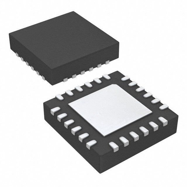
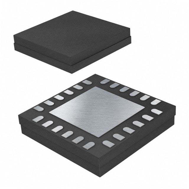
| 描述 | RF RMS PWR DETECTOR 3.9GHZ 24SMT |
| 产品分类 | |
| 品牌 | Hittite Microwave Corporation |
| 数据手册 | |
| 产品图片 |
|
| 产品型号 | HMC1010LP4E |
| RF类型 | 通用 |
| rohs | 无铅 / 符合限制有害物质指令(RoHS)规范要求 |
| 产品系列 | - |
| 其它名称 | 1127-1180-1 |
| 包装 | 剪切带 (CT) |
| 封装/外壳 | 24-VQFN 裸露焊盘 |
| 标准包装 | 1 |
| 电压-电源 | 4.5 V ~ 5.5 V |
| 电流-电源 | 50mA |
| 精度 | ±1dB |
| 输入范围 | -50dBm ~ 10dBm |
| 频率 | 0Hz ~ 3.9GHz |


- 商务部:美国ITC正式对集成电路等产品启动337调查
- 曝三星4nm工艺存在良率问题 高通将骁龙8 Gen1或转产台积电
- 太阳诱电将投资9.5亿元在常州建新厂生产MLCC 预计2023年完工
- 英特尔发布欧洲新工厂建设计划 深化IDM 2.0 战略
- 台积电先进制程称霸业界 有大客户加持明年业绩稳了
- 达到5530亿美元!SIA预计今年全球半导体销售额将创下新高
- 英特尔拟将自动驾驶子公司Mobileye上市 估值或超500亿美元
- 三星加码芯片和SET,合并消费电子和移动部门,撤换高东真等 CEO
- 三星电子宣布重大人事变动 还合并消费电子和移动部门
- 海关总署:前11个月进口集成电路产品价值2.52万亿元 增长14.8%


PDF Datasheet 数据手册内容提取
HMC1010LP4E v03.0511 RMS POWER DETECTOR DC - 3.9 GHz Typical Applications Features the HMc1010LP4e is ideal for: ±1 dB Detection Accuracy to 3.9 GHz • Log –> Root-Mean-Square (RMS) Conversion Input Dynamic range: -50 dBm to +10 dBm • Received Signal Strength Indication (RSSI) rF signal wave shape & crest Factor Independent • Transmitter Signal Strength Indication (TSSI) Digitally Programmable Integration Bandwidth • RF Power Amplifier Efficiency Control +5V operation from -40°c to +85°c • Receiver Automatic Gain Control excellent temperature stability • Transmitter Power Control Power-Down Mode 11 24 Lead 4x4mm sMt Package: 16mm² Functional Diagram General Description t the HMc1010LP4e Power Detector is designed for M rF power measurement, and control applications s for frequencies up to 3.9 GHz. the detector provides an accurate rMs representation of any rF/IF input - signal. the output is a temperature compensated s monotonic, representation of real signal power, mea- r sured with an input sensing range of 60 dB. o the HMc1010LP4e is ideally suited to those wide t c bandwidth, wide dynamic range applications, requir- e ing repeatable measurement of real signal power, t especially where rF/IF wave shape and/or crest factor e change with time. D the integration bandwidth of the HMc1010LP4e is r digitally programmable with the use of input pins scI1- e 4 with a range of more than 4 decades. this allows w the user to dynamically set the operation bandwidth providing the capability of handling different types of o modulations on the same platform. P the HMc1010LP4e features an internal oP-AMP at output stage, which provides for slope & intercept ad- justments and enables controller application. Electrical Specifications, T = +25 °C, Vcc = 5V A Parameter typ. typ. typ. typ. typ. typ. typ. Units Dynamic Range (±1dB Error) [2] Input Frequency 100 900 1900 2200 2700 3500 3900 MHz Differential Input Configuration [1] 59 64 62 62 59 49 45 dB Deviation vs Temperature: (Over full temperature range -40 °C to 85 °C). Deviation is measured from reference, which is the same wcDMA input at 25 °c. [1] Differential Input Interface with 1:1 Balun Transformer (over full input frequency range) 1 dB [2] With WCDMA 4 Carrier (TM1-64 DPCH) InforFmaotiro np fruircniseh,e dd beyl iAvnealroyg Daenvidce st ois pbelaliecveed otor dbee arcsc:u rHateit taintde reMliaibcler. oHwowaevveer, Cnoo rpFoorr aptriiocen,, d2e0liv Aerlyp, haand R too apdla,c Ce horedlemrss: fAonrdal,o gM DAe v0ic1e8s2, 4Inc., responsibility is assumed by Analog Devices for its use, nor for any infringements of patents or other One Technology Way, P.O. Box 9106, Norwood, MA 02062-9106 11 - 1 rliicgehntss eo fi sth girrda nptaerdti ebsy t himatp mlicaaPyt iorhenso uonlrt ofertoh:m e9r wit7sis 8ues -eu2.n dS5ep0re ca-inf3iyc 3aptia4otne3sn ts ou rb jpeFacttae tnoxt c:r hig9ahn7tgs 8eo wf- 2Aithn5oau0lot g-n 3oDti3ecve7i.c 3eNso . POhrodnee:r 7 O81n-3-l2i9n-e4 7a0t0 w(cid:127) wOrwde.hr oitntliitnee. cato wmww.analog.com Trademarks and registered trademarks arAe tphep plriocpearttyi oof nth eSir urepsppecotivret :o wPnehrso.ne: 978-250-3A3p4p3li c aotrio na Spuppsp@orht: iPtthitoen.ec: o1-m800-ANALOG-D
HMC1010LP4E v03.0511 RMS POWER DETECTOR DC - 3.9 GHz Electrical Specifications II, T = +25 °C, Vcc = 5V, Sci4 = Sci1 = 0V, Sci3 = Sci2 = 5V, Unless Otherwise Noted A Parameter typ. typ. typ. typ. typ. typ. typ. Units Input Frequency 100 900 1900 2200 2700 3500 3900 MHz Modulation Deviation (Output deviation from reference, which is measured with CW input at equivalent input signal power) WCDMA 4 Carrier (TM1-64 DPCH) at +25 °C 0.1 0.1 0.1 0.1 0.1 0.2 0.2 dB WCDMA 4 Carrier (TM1-64 DPCH) at +85 °C 0.1 0.1 0.1 0.1 0.1 0.1 0.2 dB WCDMA 4 Carrier (TM1-64 DPCH) at -40 °C 0.1 0.1 0.1 0.1 0.1 0.1 0.2 dB Logarithmic Slope and Intercept [1] Logarithmic slope 36.4 36.6 37.3 37.8 39 43.3 47.7 mV/dB Logarithmic Intercept -70.1 -69.1 -67.6 -66.3 -63.1 -55 -51 dBm 11 Max. Input Power at ±1dB error 4 10 10 10 6 5 4 dBm Min. Input Power at ±1dB error -55 -54 -52 -52 -49 -44 -41 dBm [1] With WCDMA 4 Carrier (TM1-64 DPCH) t M s RMSOUT vs. Pin with Different RMSOUT Error vs. Pin with Different Modulations @ 1900 MHz [1] Modulations @ 1900 MHz [1] - s 4 4 r 3.5 Ideal 3 o CW 3 CDMA2000 4 carriers 2 LTE DOWN t WCDMA 4 carriers V)2.5 WCDMA single carrier B) 1 c UT ( 2 R (d 0 e O O S R t RM1.5 ER -1 e 1 -2 CCWDMA2000 4 carriers D LTE DOWN 0.5 -3 WCDMA 4 carriers WCDMA single carrier r 0 -4 e -60 -50 -40 -30 -20 -10 0 10 -60 -50 -40 -30 -20 -10 0 10 w INPUT POWER (dBm) INPUT POWER (dBm) o P [1] Data was taken at sci4=sci1=0V, sci3=sci2=5V, shortest integration time is for scI=0000, allowed longest integration time is for scI=1100 InforFmaotiro np fruircniseh,e dd beyl iAvnealroyg Daenvidce st ois pbelaliecveed otor dbee arcsc:u rHateit taintde reMliaibcler. oHwowaevveer, Cnoo rpFoorr aptriiocen,, d2e0liv Aerlyp, haand R too apdla,c Ce horedlemrss: fAonrdal,o gM DAe v0ic1e8s2, 4Inc., responsibility is assumed by Analog Devices for its use, nor for any infringements of patents or other One Technology Way, P.O. Box 9106, Norwood, MA 02062-9106 rights of third parties that maPy rhesounlt fero:m 9 it7s 8us-e2. S5p0ec-if3ic3ati4on3s s u b jeFcta tox c: h9an7g8e w-2ith5ou0t -n3oti3ce7. 3No POhrodnee:r 7 O81n-3-l2i9n-e4 7a0t0 w(cid:127) wOrwde.hr oitntliitnee. cato wmww.analog.com 11 - 2 license is granted by implication or otherwise under any patent or patent rights of Analog Devices. Trademarks and registered trademarks arAe tphep plriocpearttyi oof nth eSir urepsppecotivret :o wPnehrso.ne: 978-250-3A3p4p3li c aotrio na Spuppsp@orht: iPtthitoen.ec: o1-m800-ANALOG-D
HMC1010LP4E v03.0511 RMS POWER DETECTOR DC - 3.9 GHz Electrical Specifications III, TA = +25 °C, Vcc = 5V, Sci4 = Sci1 = 0V, Sci3 = Sci2 = 5V, Unless Otherwise Noted Parameter conditions Min typ. Max Units Differential Input Configuration Input Network return Loss up to 2.5 GHz [1] > 10 dB Input resistance between IN+ and IN- Between pins 3 and 4 150 Ω Input Voltage range V = V - V 1.6 V DIFFIN IN+ IN- RMSOUT Output output Voltage range 0.4 to 2.9 V source/sink current compliance rMsoUt held at Vcc/2 8 / -0.524 mA 11 Output Slew Rate (rise / fall) sci4=sci3=sci2=sci1=0V, cofs=1nF 17.92 / 1.41 106 V/s VSET Input (Negative Feedback Terminal) For control applications with nominal Input Voltage range 0.4 to 2.9 V slope/intercept settings t Input resistance 5 MΩ M SCI1-4 Inputs, ENX Logic Input (Power Down Control) s Input High Voltage 0.7xVcc V Input Low Voltage 0.3xVcc V - Input High current 1 μA s Input Low current 1 μA r Input capacitance 0.5 pF o Power Supply t supply Voltage 4.5 5 5.5 V c 40 mA typical at -40 °c, e supply current with no input power 54.5 mA typical at 85 °c 47.5 mA t 42 mA typical at -40 °c, supply current with Pin = 0 dBm 50 mA e 57 mA typical at 85 °c D standby Mode supply current 5 mA [1] Performance of differential input configuration is limited by the balun. Baluns used is M/A-COM ETC1-1-13 specified over 4.5 to 3000 MHz r e w o P InforFmaotiro np fruircniseh,e dd beyl iAvnealroyg Daenvidce st ois pbelaliecveed otor dbee arcsc:u rHateit taintde reMliaibcler. oHwowaevveer, Cnoo rpFoorr aptriiocen,, d2e0liv Aerlyp, haand R too apdla,c Ce horedlemrss: fAonrdal,o gM DAe v0ic1e8s2, 4Inc., responsibility is assumed by Analog Devices for its use, nor for any infringements of patents or other One Technology Way, P.O. Box 9106, Norwood, MA 02062-9106 11 - 3 rliicgehntss eo fi sth girrda nptaerdti ebsy t himatp mlicaaPyt iorhenso uonlrt ofertoh:m e9r wit7sis 8ues -eu2.n dS5ep0re ca-inf3iyc 3aptia4otne3sn ts ou rb jpeFacttae tnoxt c:r hig9ahn7tgs 8eo wf- 2Aithn5oau0lot g-n 3oDti3ecve7i.c 3eNso . POhrodnee:r 7 O81n-3-l2i9n-e4 7a0t0 w(cid:127) wOrwde.hr oitntliitnee. cato wmww.analog.com Trademarks and registered trademarks arAe tphep plriocpearttyi oof nth eSir urepsppecotivret :o wPnehrso.ne: 978-250-3A3p4p3li c aotrio na Spuppsp@orht: iPtthitoen.ec: o1-m800-ANALOG-D
HMC1010LP4E v03.0511 RMS POWER DETECTOR DC - 3.9 GHz RMSOUT & Error vs. Pin @ 100 MHz [1][2] RMSOUT & Error vs. Pin @ 900 MHz [1][2] 3.2 4 3.2 4 2.8 3 2.8 3 ERR +25 C ERR +25 C 2.4 EERRRR +-4805 CC 2 2.4 EERRRR +-4805 CC 2 V) 2 1 E V) 2 1 E RMSOUT (11..26 -01 RROR (dB RMSOUT (11..26 -01 RROR (dB ) ) 0.8 Ideal -2 0.8 Ideal -2 LOGOUT +25 C LOGOUT +25 C 0.4 LOGOUT +85 C -3 0.4 LOGOUT +85 C -3 11 LOGOUT -40 C LOGOUT -40 C 0 -4 0 -4 -60 -50 -40 -30 -20 -10 0 10 -60 -50 -40 -30 -20 -10 0 10 INPUT POWER (dBm) INPUT POWER (dBm) t M s RMSOUT & Error vs. Pin @ 1900 MHz [1][2] RMSOUT & Error vs. Pin @ 2200 MHz [1][2] - 3.2 4 3.2 4 s 2.8 3 2.8 3 ERR +25 C ERR +25 C r ERR +85 C ERR +85 C 2.4 ERR -40 C 2 2.4 ERR -40 C 2 o V) 2 1 E V) 2 1 E t RMSOUT (11..26 -01 RROR (dB) RMSOUT (11..26 -01 RROR (dB) tec 0.8 -2 0.8 -2 e Ideal Ideal LOGOUT +25 C LOGOUT +25 C 0.4 LOGOUT +85 C -3 0.4 LOGOUT +85 C -3 D LOGOUT -40 C LOGOUT -40 C 0 -4 0 -4 r -60 -50 -40 -30 -20 -10 0 10 -60 -50 -40 -30 -20 -10 0 10 e INPUT POWER (dBm) INPUT POWER (dBm) w o P RMSOUT & Error vs. Pin @ 2700 MHz [1][2] RMSOUT & Error vs. Pin @ 3500 MHz [1][2] 3.2 4 3.2 4 2.8 3 2.8 3 ERR +25 C ERR +25 C ERR +85 C ERR +85 C 2.4 ERR -40 C 2 2.4 ERR -40 C 2 V) 2 1 E V) 2 1 E RMSOUT (11..26 -01 RROR (dB RMSOUT (11..26 -01 RROR (dB ) ) 0.8 -2 0.8 -2 Ideal Ideal LOGOUT +25 C LOGOUT +25 C 0.4 LOGOUT +85 C -3 0.4 LOGOUT +85 C -3 LOGOUT -40 C LOGOUT -40 C 0 -4 0 -4 -60 -50 -40 -30 -20 -10 0 10 -60 -50 -40 -30 -20 -10 0 10 INPUT POWER (dBm) INPUT POWER (dBm) [1] Data was taken at sci4=sci1=0V, sci3=sci2=5V, shortest integration time is for scI=0000, allowed longest integration time is for scI=1100 [2] wcDMA 4 carriers input waveform InforFmaotiro np fruircniseh,e dd beyl iAvnealroyg Daenvidce st ois pbelaliecveed otor dbee arcsc:u rHateit taintde reMliaibcler. oHwowaevveer, Cnoo rpFoorr aptriiocen,, d2e0liv Aerlyp, haand R too apdla,c Ce horedlemrss: fAonrdal,o gM DAe v0ic1e8s2, 4Inc., responsibility is assumed by Analog Devices for its use, nor for any infringements of patents or other One Technology Way, P.O. Box 9106, Norwood, MA 02062-9106 rights of third parties that maPy rhesounlt fero:m 9 it7s 8us-e2. S5p0ec-if3ic3ati4on3s s u b jeFcta tox c: h9an7g8e w-2ith5ou0t -n3oti3ce7. 3No POhrodnee:r 7 O81n-3-l2i9n-e4 7a0t0 w(cid:127) wOrwde.hr oitntliitnee. cato wmww.analog.com 11 - 4 license is granted by implication or otherwise under any patent or patent rights of Analog Devices. Trademarks and registered trademarks arAe tphep plriocpearttyi oof nth eSir urepsppecotivret :o wPnehrso.ne: 978-250-3A3p4p3li c aotrio na Spuppsp@orht: iPtthitoen.ec: o1-m800-ANALOG-D
HMC1010LP4E v03.0511 RMS POWER DETECTOR DC - 3.9 GHz RMSOUT & Error vs. Pin @ 3900 MHz [1][2] Intercept vs. Frequency [1][2] 3.2 4 -40 2.8 3 -45 ERR +25 C +25C ERR +85 C +85C 2.4 ERR -40 C 2 m)-50 -40C B RMSOUT (V)11..262 -011 ERROR (dB TERCEPT (d---665505 ) N 0.8 -2 I-70 Ideal 11 0.4 LLOOGGOOUUTT ++2855 CC -3 -75 LOGOUT -40 C 0 -4 -80 0 500 1000 1500 2000 2500 3000 3500 4000 -60 -50 -40 -30 -20 -10 0 10 FREQUENCY (MHz) INPUT POWER (dBm) t M RMSOUT vs. Pin with WCDMA s Slope vs. Frequency [1][2] 4 Carrier @ +25 °C [1] - 60 3 s 100 MHz r 55 2.5 900 MHz 1900 MHz ecto OPE (mV/dB) 4550 ++ -284550CCC MSOUT (V) 1.52 2233275900000000 MMMMHHHHzzzz t SL 40 R 1 e 35 0.5 D r 300 500 1000 1500 2000 2500 3000 3500 4000 0-70 -60 -50 -40 -30 -20 -10 0 10 e FREQUENCY (MHz) INPUT POWER (dBm) w o RMSOUT Error vs. Pin with WCDMA 4 RMSOUT Error vs. Pin with WCDMA 4 P Carrier @ +25 °C [1] Carrier @ +85 °C wrt +25 °C Response [1] 4 4 3 3 2 2 B) 1 B) 1 d d OR ( 0 OR ( 0 R R R R E -1 E -1 100 MHz 100 MHz 900 MHz 900 MHz 1900 MHz -2 1900 MHz -2 2200 MHz 2200 MHz 2700 MHz -3 23750000 MMHHzz -3 33590000 MMHHzz 3900 MHz -4 -4 -60 -50 -40 -30 -20 -10 0 10 -70 -60 -50 -40 -30 -20 -10 0 10 INPUT POWER (dBm) INPUT POWER (dBm) [1] Data was taken at sci4=sci1=0V, sci3=sci2=5V, shortest integration time is for scI=0000, allowed longest integration time is for scI=1100 [2] wcDMA 4 carriers input waveform InforFmaotiro np fruircniseh,e dd beyl iAvnealroyg Daenvidce st ois pbelaliecveed otor dbee arcsc:u rHateit taintde reMliaibcler. oHwowaevveer, Cnoo rpFoorr aptriiocen,, d2e0liv Aerlyp, haand R too apdla,c Ce horedlemrss: fAonrdal,o gM DAe v0ic1e8s2, 4Inc., responsibility is assumed by Analog Devices for its use, nor for any infringements of patents or other One Technology Way, P.O. Box 9106, Norwood, MA 02062-9106 11 - 5 rliicgehntss eo fi sth girrda nptaerdti ebsy t himatp mlicaaPyt iorhenso uonlrt ofertoh:m e9r wit7sis 8ues -eu2.n dS5ep0re ca-inf3iyc 3aptia4otne3sn ts ou rb jpeFacttae tnoxt c:r hig9ahn7tgs 8eo wf- 2Aithn5oau0lot g-n 3oDti3ecve7i.c 3eNso . POhrodnee:r 7 O81n-3-l2i9n-e4 7a0t0 w(cid:127) wOrwde.hr oitntliitnee. cato wmww.analog.com Trademarks and registered trademarks arAe tphep plriocpearttyi oof nth eSir urepsppecotivret :o wPnehrso.ne: 978-250-3A3p4p3li c aotrio na Spuppsp@orht: iPtthitoen.ec: o1-m800-ANALOG-D
HMC1010LP4E v03.0511 RMS POWER DETECTOR DC - 3.9 GHz RMSOUT Error vs. Pin with WCDMA 4 Carrier @ -40 °C wrt +25 °C Response [1] RMSOUT vs. Pin with CW @ +25 °C [1] 4 3 3 100 MHz 2.5 900 MHz 1900 MHz 2 2200 MHz OR (dB) 01 OUT (V) 1.52 233759000000 MMMHHHzzz RR MS E -1 100 MHz R 900 MHz 1 1900 MHz -2 2200 MHz 2700 MHz 0.5 -3 3500 MHz 11 3900 MHz -4 0 -70 -60 -50 -40 -30 -20 -10 0 10 -70 -60 -50 -40 -30 -20 -10 0 10 INPUT POWER (dBm) INPUT POWER (dBm) t M RMSOUT vs. Pin w/ CW & WCDMA 4 Carrier s RMSOUT Error vs. Pin with CW @ +25 °C [1] (TM1-64 DPCH) @ 1900 MHz & +25 °C [1] - 4 3 s 3 2.5 r 2 o OR (dB) 01 OUT (V) 1.52 ct RR MS e E -1 R 100 MHz 1 t 900 MHz -2 1900 MHz e -3 223275000000 MMMHHHzzz 0.5 CWWCDMA D 3900 MHz -4-60 -50 -40 -30 -20 -10 0 10 0-70 -60 -50 -40 -30 -20 -10 0 10 r INPUT POWER (dBm) INPUT POWER (dBm) e w o Reading Error for WCDMA 4 Carrier wrt RMSOUT vs. Pin w/ CW & WCDMA 4 Carrier P CW Response @ +25 °C [1] (TM1-64 DPCH) @ 1900 MHz & +85 °C [1] 1 3 0.8 2.5 0.6 ROR (dB) 00..240 MSOUT (V) 1.52 ER-0.2 100 MHz R 1 -0.4 900 MHz 1900 MHz -0.6 22270000 MMHHzz 0.5 CWWCDMA -0.8 3500 MHz 3900 MHz -1 0 -70 -60 -50 -40 -30 -20 -10 0 10 -70 -60 -50 -40 -30 -20 -10 0 10 INPUT POWER (dBm) INPUT POWER (dBm) [1] Data was taken at sci4=sci1=0V, sci3=sci2=5V, shortest integration time is for scI=0000, allowed longest integration time is for scI=1100 InforFmaotiro np fruircniseh,e dd beyl iAvnealroyg Daenvidce st ois pbelaliecveed otor dbee arcsc:u rHateit taintde reMliaibcler. oHwowaevveer, Cnoo rpFoorr aptriiocen,, d2e0liv Aerlyp, haand R too apdla,c Ce horedlemrss: fAonrdal,o gM DAe v0ic1e8s2, 4Inc., responsibility is assumed by Analog Devices for its use, nor for any infringements of patents or other One Technology Way, P.O. Box 9106, Norwood, MA 02062-9106 rights of third parties that maPy rhesounlt fero:m 9 it7s 8us-e2. S5p0ec-if3ic3ati4on3s s u b jeFcta tox c: h9an7g8e w-2ith5ou0t -n3oti3ce7. 3No POhrodnee:r 7 O81n-3-l2i9n-e4 7a0t0 w(cid:127) wOrwde.hr oitntliitnee. cato wmww.analog.com 11 - 6 license is granted by implication or otherwise under any patent or patent rights of Analog Devices. Trademarks and registered trademarks arAe tphep plriocpearttyi oof nth eSir urepsppecotivret :o wPnehrso.ne: 978-250-3A3p4p3li c aotrio na Spuppsp@orht: iPtthitoen.ec: o1-m800-ANALOG-D
HMC1010LP4E v03.0511 RMS POWER DETECTOR DC - 3.9 GHz Reading Error for WCDMA 4 Carrier wrt RMSOUT vs. Pin w/ CW & WCDMA 4 Carrier CW Response @ +85 °C [1] (TM1-64 DPCH) @ 1900 MHz & -40 °C [1] 1 3 0.8 2.5 0.6 OR (dB) 00..240 OUT (V) 1.52 CWWCDMA ERR-0.2 100 MHz RMS 1 -0.4 900 MHz 1900 MHz -0.6 2200 MHz 2700 MHz 0.5 11 -0.8 33590000 MMHHzz -1 0 -70 -60 -50 -40 -30 -20 -10 0 10 -70 -60 -50 -40 -30 -20 -10 0 10 INPUT POWER (dBm) INPUT POWER (dBm) t M Reading Error for WCDMA 4 Carrier wrt Output Response s CW Response @ -40 °C [1] with SCI = 0000 @ 1900 MHz - 1 3 25 s 0.8 r 2.5 RMSOUT 20 0.6 R o F tect ERROR (dB)--0000....42240 190000 MMHHzz RMSOUT (V)1.512 - 2 00 ddBBmm 51105 ENABLE VOLTAG e -0.6 122927000000 MMMHHHzzz 0.5 ORFFF ORNF ORFFF RF ENABLE 0 E (V D -0.8 33590000 MMHHzz ) r -1 0 -5 -70 -60 -50 -40 -30 -20 -10 0 10 -2 0 2 4 6 8 10 12 14 16 18 e INPUT POWER (dBm) TIME (μs) w o P Typical Supply Current vs. Pin, Vcc = 5V 60 A) 55 m T ( N E 50 R R U C LY 45 ++2855 CC P -40 C P U S 40 35 -70 -60 -50 -40 -30 -20 -10 0 10 INPUT POWER (dBm) [1] Data was taken at sci4=sci1=0V, sci3=sci2=5V, shortest integration time is for scI=0000, allowed longest integration time is for scI=1100 InforFmaotiro np fruircniseh,e dd beyl iAvnealroyg Daenvidce st ois pbelaliecveed otor dbee arcsc:u rHateit taintde reMliaibcler. oHwowaevveer, Cnoo rpFoorr aptriiocen,, d2e0liv Aerlyp, haand R too apdla,c Ce horedlemrss: fAonrdal,o gM DAe v0ic1e8s2, 4Inc., responsibility is assumed by Analog Devices for its use, nor for any infringements of patents or other One Technology Way, P.O. Box 9106, Norwood, MA 02062-9106 11 - 7 rliicgehntss eo fi sth girrda nptaerdti ebsy t himatp mlicaaPyt iorhenso uonlrt ofertoh:m e9r wit7sis 8ues -eu2.n dS5ep0re ca-inf3iyc 3aptia4otne3sn ts ou rb jpeFacttae tnoxt c:r hig9ahn7tgs 8eo wf- 2Aithn5oau0lot g-n 3oDti3ecve7i.c 3eNso . POhrodnee:r 7 O81n-3-l2i9n-e4 7a0t0 w(cid:127) wOrwde.hr oitntliitnee. cato wmww.analog.com Trademarks and registered trademarks arAe tphep plriocpearttyi oof nth eSir urepsppecotivret :o wPnehrso.ne: 978-250-3A3p4p3li c aotrio na Spuppsp@orht: iPtthitoen.ec: o1-m800-ANALOG-D
HMC1010LP4E v03.0511 RMS POWER DETECTOR DC - 3.9 GHz Output Ripple & Rise/Fall Time vs. Integration Setting Input Return Loss vs. Frequency [Sci4,Sci3,Sci2,Sci1] in Decimal 0 1800 100000 RETURN LOSS (dB)-----32211-050505 DM4.e/5Af iMn-CeHodzm int ob l aa3rl0ug0ne0 #p MEarTHt Czb1y- b1a-1lu1n3:; Output Ripple Peak-Peak (mV)11369250000000000 RRRRiiiipppppppplllleeee wwwwiiiitttthhhh WW88 TTCCooDDnnMMee AA((1141k0TTHkMMHz zs espeepreartaiotino)nRF)aislle T Timimee 11111000000000Rise Time & Fall Time (us)0 11 -35 0 0.1 0 1 2 3 4 5 6 0 1 2 3 4 5 6 7 8 9 10 11 12 FREQUENCY (GHz) Integration Setting (in Decimal) t M s - s r o t c e t e D r e w o P InforFmaotiro np fruircniseh,e dd beyl iAvnealroyg Daenvidce st ois pbelaliecveed otor dbee arcsc:u rHateit taintde reMliaibcler. oHwowaevveer, Cnoo rpFoorr aptriiocen,, d2e0liv Aerlyp, haand R too apdla,c Ce horedlemrss: fAonrdal,o gM DAe v0ic1e8s2, 4Inc., responsibility is assumed by Analog Devices for its use, nor for any infringements of patents or other One Technology Way, P.O. Box 9106, Norwood, MA 02062-9106 rights of third parties that maPy rhesounlt fero:m 9 it7s 8us-e2. S5p0ec-if3ic3ati4on3s s u b jeFcta tox c: h9an7g8e w-2ith5ou0t -n3oti3ce7. 3No POhrodnee:r 7 O81n-3-l2i9n-e4 7a0t0 w(cid:127) wOrwde.hr oitntliitnee. cato wmww.analog.com 11 - 8 license is granted by implication or otherwise under any patent or patent rights of Analog Devices. Trademarks and registered trademarks arAe tphep plriocpearttyi oof nth eSir urepsppecotivret :o wPnehrso.ne: 978-250-3A3p4p3li c aotrio na Spuppsp@orht: iPtthitoen.ec: o1-m800-ANALOG-D
HMC1010LP4E v03.0511 RMS POWER DETECTOR DC - 3.9 GHz Absolute Maximum Ratings Supply Voltage (Vcc) 5.6V eLectrostAtIc seNsItIVe DeVIce rF Input Power 16 dBm oBserVe HANDLING PrecAUtIoNs Differential Input Voltage 1.6 Vp-p channel / Junction temperature 125 °c Continuous Pdiss (T = 85°C) 1.39 w (Derate 34.87 mW/°c above 85°C) Thermal Resistance (R ) th 28.68 °c/w (junction to ground paddle) storage temperature -65 to +150 °c 11 operating temperature -40 to +85 °c ESD Sensitivity (HBM) class 1B t Outline Drawing M s - s r o t c e t e D r e w o P Notes: 1. LeADFrAMe MAterIAL: coPPer ALLoY 2. DIMeNsIoNs Are IN INcHes [MILLIMeters]. 3. LeAD sPAcING toLerANce Is NoN-cUMULAtIVe 4. PAD BUrr LeNGtH sHALL Be 0.15mm MAXIMUM. PAD BUrr HeIGHt sHALL Be 0.05mm MAXIMUM. 5. PAcKAGe wArP sHALL Not eXceeD 0.05mm. 6. ALL GroUND LeADs AND GroUND PADDLe MUst Be soLDereD to PcB rF GroUND. 7. reFer to HMc APPLIcAtIoN Note For sUGGesteD PcB LAND PAtterN. Package Information Part Number Package Body Material Lead Finish MsL rating Package Marking [1] HMc1010LP4e roHs-compliant Low stress Injection Molded Plastic 100% matte sn MsL1 [2] H1010 XXXX [1] 4-Digit lot number XXXX [2] Max peak reflow temperature of 260 °c InforFmaotiro np fruircniseh,e dd beyl iAvnealroyg Daenvidce st ois pbelaliecveed otor dbee arcsc:u rHateit taintde reMliaibcler. oHwowaevveer, Cnoo rpFoorr aptriiocen,, d2e0liv Aerlyp, haand R too apdla,c Ce horedlemrss: fAonrdal,o gM DAe v0ic1e8s2, 4Inc., responsibility is assumed by Analog Devices for its use, nor for any infringements of patents or other One Technology Way, P.O. Box 9106, Norwood, MA 02062-9106 11 - 9 rliicgehntss eo fi sth girrda nptaerdti ebsy t himatp mlicaaPyt iorhenso uonlrt ofertoh:m e9r wit7sis 8ues -eu2.n dS5ep0re ca-inf3iyc 3aptia4otne3sn ts ou rb jpeFacttae tnoxt c:r hig9ahn7tgs 8eo wf- 2Aithn5oau0lot g-n 3oDti3ecve7i.c 3eNso . POhrodnee:r 7 O81n-3-l2i9n-e4 7a0t0 w(cid:127) wOrwde.hr oitntliitnee. cato wmww.analog.com Trademarks and registered trademarks arAe tphep plriocpearttyi oof nth eSir urepsppecotivret :o wPnehrso.ne: 978-250-3A3p4p3li c aotrio na Spuppsp@orht: iPtthitoen.ec: o1-m800-ANALOG-D
HMC1010LP4E v03.0511 RMS POWER DETECTOR DC - 3.9 GHz Pin Descriptions Pin Number Function Description Interface schematic Power supply. connect supply voltage to these 1, 16, 21, 23 Vcc pins with appropriate filtering. 11 2, 5, 6, 8, Package bottom has an exposed metal paddle that 11 - 13, 22, 24 GND must be connected to rF/Dc ground. Package Base t M s - s r o t rF input pins. connect rF to c 3, 4 IN+, IN- IN+ and IN- through a 1:1 balun e t e D r e w o P Disable pin. connect to GND for normal operation. 7 eNX Applying voltage V>0.8xVcc will initiate power saving mode InforFmaotiro np fruircniseh,e dd beyl iAvnealroyg Daenvidce st ois pbelaliecveed otor dbee arcsc:u rHateit taintde reMliaibcler. oHwowaevveer, Cnoo rpFoorr aptriiocen,, d2e0liv Aerlyp, haand R too apdla,c Ce horedlemrss: fAonrdal,o gM DAe v0ic1e8s2, 4Inc., responsibility is assumed by Analog Devices for its use, nor for any infringements of patents or other One Technology Way, P.O. Box 9106, Norwood, MA 02062-9106 rights of third parties that maPy rhesounlt fero:m 9 it7s 8us-e2. S5p0ec-if3ic3ati4on3s s u b jeFcta tox c: h9an7g8e w-2ith5ou0t -n3oti3ce7. 3No POhrodnee:r 7 O81n-3-l2i9n-e4 7a0t0 w(cid:127) wOrwde.hr oitntliitnee. cato wmww.analog.com 11 - 10 license is granted by implication or otherwise under any patent or patent rights of Analog Devices. Trademarks and registered trademarks arAe tphep plriocpearttyi oof nth eSir urepsppecotivret :o wPnehrso.ne: 978-250-3A3p4p3li c aotrio na Spuppsp@orht: iPtthitoen.ec: o1-m800-ANALOG-D
HMC1010LP4E v03.0511 RMS POWER DETECTOR DC - 3.9 GHz Pin Descriptions (Continued) Pin Number Function Description Interface schematic High pass filter capacitor input. Connect a coFsA, 9, 10 capacitor between coFsA and coFsB to coFsB determine 3 dB point of input signal high-pass filter. 11 t M s 14 Vset setpoint input for controller mode. Allows change of output slope resulting in output power leveling. - s r o t Logarithmic output that provides an c 15 rMsoUt indication of mean square input power. e t e D Digitally Programmable Integration Bandwidth r control. Input pins that control the internal integration time constant for rMs calculation. scI4 e is the most significant bit. Set V>0.8xVcc to enable w 17 - 20 scI1 - scI4 and V<0.2xVcc to disable (active high). Shortest integration time is for scI=0000, allowed longest o integration time is for SCI=1100 (1101, 1110 and P 1111 SCI settings are forbidden states). Each step changes the integration time by 1 octave. InforFmaotiro np fruircniseh,e dd beyl iAvnealroyg Daenvidce st ois pbelaliecveed otor dbee arcsc:u rHateit taintde reMliaibcler. oHwowaevveer, Cnoo rpFoorr aptriiocen,, d2e0liv Aerlyp, haand R too apdla,c Ce horedlemrss: fAonrdal,o gM DAe v0ic1e8s2, 4Inc., responsibility is assumed by Analog Devices for its use, nor for any infringements of patents or other One Technology Way, P.O. Box 9106, Norwood, MA 02062-9106 11 - 11 rliicgehntss eo fi sth girrda nptaerdti ebsy t himatp mlicaaPyt iorhenso uonlrt ofertoh:m e9r wit7sis 8ues -eu2.n dS5ep0re ca-inf3iyc 3aptia4otne3sn ts ou rb jpeFacttae tnoxt c:r hig9ahn7tgs 8eo wf- 2Aithn5oau0lot g-n 3oDti3ecve7i.c 3eNso . POhrodnee:r 7 O81n-3-l2i9n-e4 7a0t0 w(cid:127) wOrwde.hr oitntliitnee. cato wmww.analog.com Trademarks and registered trademarks arAe tphep plriocpearttyi oof nth eSir urepsppecotivret :o wPnehrso.ne: 978-250-3A3p4p3li c aotrio na Spuppsp@orht: iPtthitoen.ec: o1-m800-ANALOG-D
HMC1010LP4E v03.0511 RMS POWER DETECTOR DC - 3.9 GHz Application Circuit - Differential Configuration 11 t M s - s r o t c e t e D r e w o P InforFmaotiro np fruircniseh,e dd beyl iAvnealroyg Daenvidce st ois pbelaliecveed otor dbee arcsc:u rHateit taintde reMliaibcler. oHwowaevveer, Cnoo rpFoorr aptriiocen,, d2e0liv Aerlyp, haand R too apdla,c Ce horedlemrss: fAonrdal,o gM DAe v0ic1e8s2, 4Inc., responsibility is assumed by Analog Devices for its use, nor for any infringements of patents or other One Technology Way, P.O. Box 9106, Norwood, MA 02062-9106 rights of third parties that maPy rhesounlt fero:m 9 it7s 8us-e2. S5p0ec-if3ic3ati4on3s s u b jeFcta tox c: h9an7g8e w-2ith5ou0t -n3oti3ce7. 3No POhrodnee:r 7 O81n-3-l2i9n-e4 7a0t0 w(cid:127) wOrwde.hr oitntliitnee. cato wmww.analog.com 11 - 12 license is granted by implication or otherwise under any patent or patent rights of Analog Devices. Trademarks and registered trademarks arAe tphep plriocpearttyi oof nth eSir urepsppecotivret :o wPnehrso.ne: 978-250-3A3p4p3li c aotrio na Spuppsp@orht: iPtthitoen.ec: o1-m800-ANALOG-D
HMC1010LP4E v03.0511 RMS POWER DETECTOR DC - 3.9 GHz Evaluation PCB - Differential Configuration 11 t M s - s r o t c e t e D r e w List of Materials for Evaluation PCB 128694 [1] o the circuit board used in the application should Item Description P use rF circuit design techniques. signal lines sho- J1, J2 Pc Mount sMA connector uld have 50 ohm impedance while the package tP1 - tP9 Dc Pin ground leads and exposed paddle should be con- c1, c10, c16 100 pF capacitor, 0402 Pkg. nected directly to the ground plane similar to that c3, c4, c6 1000 pF capacitor, 0402 Pkg. shown. A sufficient number of via holes should be c2, c5, c11, c17 100 nF capacitor, 0402 Pkg. used to connect the top and bottom ground planes. r1 68 ohm resistor, 0402 Pkg. the evaluation circuit board shown is available from r2, r12 - r15 10 k resistor, 0402 Pkg. Hittite upon request. r3, r9, r10 0 ohm resistor, 0402 Pkg. r6, r7 4.7 k resistor, 0402 Pkg. t1 1:1 Balun, M/A-coM etc1-1-13 HMc1010LP4e U1 rMs Power Detector PcB [2] 128691 evaluation PcB [1] reference this number when ordering complete evaluation PcB [2] circuit Board Material: rogers 4350 InforFmaotiro np fruircniseh,e dd beyl iAvnealroyg Daenvidce st ois pbelaliecveed otor dbee arcsc:u rHateit taintde reMliaibcler. oHwowaevveer, Cnoo rpFoorr aptriiocen,, d2e0liv Aerlyp, haand R too apdla,c Ce horedlemrss: fAonrdal,o gM DAe v0ic1e8s2, 4Inc., responsibility is assumed by Analog Devices for its use, nor for any infringements of patents or other One Technology Way, P.O. Box 9106, Norwood, MA 02062-9106 11 - 13 rliicgehntss eo fi sth girrda nptaerdti ebsy t himatp mlicaaPyt iorhenso uonlrt ofertoh:m e9r wit7sis 8ues -eu2.n dS5ep0re ca-inf3iyc 3aptia4otne3sn ts ou rb jpeFacttae tnoxt c:r hig9ahn7tgs 8eo wf- 2Aithn5oau0lot g-n 3oDti3ecve7i.c 3eNso . POhrodnee:r 7 O81n-3-l2i9n-e4 7a0t0 w(cid:127) wOrwde.hr oitntliitnee. cato wmww.analog.com Trademarks and registered trademarks arAe tphep plriocpearttyi oof nth eSir urepsppecotivret :o wPnehrso.ne: 978-250-3A3p4p3li c aotrio na Spuppsp@orht: iPtthitoen.ec: o1-m800-ANALOG-D
HMC1010LP4E v03.0511 RMS POWER DETECTOR DC - 3.9 GHz Application Circuit - Single-Ended Configuration, 900 MHz Tune 11 t M s - s r o t c e t e D r Note: For the values of c3, c4, r4, r10, r11, L1, refer to single-ended Input Interface in Application Information e w o P InforFmaotiro np fruircniseh,e dd beyl iAvnealroyg Daenvidce st ois pbelaliecveed otor dbee arcsc:u rHateit taintde reMliaibcler. oHwowaevveer, Cnoo rpFoorr aptriiocen,, d2e0liv Aerlyp, haand R too apdla,c Ce horedlemrss: fAonrdal,o gM DAe v0ic1e8s2, 4Inc., responsibility is assumed by Analog Devices for its use, nor for any infringements of patents or other One Technology Way, P.O. Box 9106, Norwood, MA 02062-9106 rights of third parties that maPy rhesounlt fero:m 9 it7s 8us-e2. S5p0ec-if3ic3ati4on3s s u b jeFcta tox c: h9an7g8e w-2ith5ou0t -n3oti3ce7. 3No POhrodnee:r 7 O81n-3-l2i9n-e4 7a0t0 w(cid:127) wOrwde.hr oitntliitnee. cato wmww.analog.com 11 - 14 license is granted by implication or otherwise under any patent or patent rights of Analog Devices. Trademarks and registered trademarks arAe tphep plriocpearttyi oof nth eSir urepsppecotivret :o wPnehrso.ne: 978-250-3A3p4p3li c aotrio na Spuppsp@orht: iPtthitoen.ec: o1-m800-ANALOG-D
HMC1010LP4E v03.0511 RMS POWER DETECTOR DC - 3.9 GHz Evaluation PCB - Single-Ended Configuration, 900 MHz Tune 11 t M s - s r o t c e t e D r List of Materials for Evaluation PCB 130436 [1] e the circuit board used in the application should Item Description w use rF circuit design techniques. signal lines sho- J1, J2 sMA connector o uld have 50 ohm impedance while the package tP1 - tP9 Dc Pin P ground leads and exposed paddle should be con- c1, c3, c10, c16 100 pF capacitor, 0402 Pkg. nected directly to the ground plane similar to that c2, c5, c11, c17 100 nF capacitor, 0402 Pkg. shown. A sufficient number of via holes should be c4 5.6 pF capacitor, 0402 Pkg. used to connect the top and bottom ground planes. c6 1000 pF capacitor, 0402 Pkg. the evaluation circuit board shown is available from r2, r12 - r15 10 k resistor, 0402 Pkg. Hittite upon request. r3, r5, r9, r10 0 ohm resistor, 0402 Pkg. r4 27 ohm resistor, 0402 Pkg. Board is configured with single-ended interface r6, r7 4.7 k resistor, 0402 Pkg. suitable for input signal frequencies at 900 MHz. r11 82 ohm resistor, 0402 Pkg. refer to section on tuning single-ended interface in L1 6.8 nH Inductor, 0402 Pkg. application information for operating with signals at U1 HMc1010LP4e other frequencies. rMs Power Detector PcB [3] 128683 evaluation PcB [1] reference this number when ordering complete evaluation PcB [2] circuit Board Material: rogers 4350 InforFmaotiro np fruircniseh,e dd beyl iAvnealroyg Daenvidce st ois pbelaliecveed otor dbee arcsc:u rHateit taintde reMliaibcler. oHwowaevveer, Cnoo rpFoorr aptriiocen,, d2e0liv Aerlyp, haand R too apdla,c Ce horedlemrss: fAonrdal,o gM DAe v0ic1e8s2, 4Inc., responsibility is assumed by Analog Devices for its use, nor for any infringements of patents or other One Technology Way, P.O. Box 9106, Norwood, MA 02062-9106 11 - 15 rliicgehntss eo fi sth girrda nptaerdti ebsy t himatp mlicaaPyt iorhenso uonlrt ofertoh:m e9r wit7sis 8ues -eu2.n dS5ep0re ca-inf3iyc 3aptia4otne3sn ts ou rb jpeFacttae tnoxt c:r hig9ahn7tgs 8eo wf- 2Aithn5oau0lot g-n 3oDti3ecve7i.c 3eNso . POhrodnee:r 7 O81n-3-l2i9n-e4 7a0t0 w(cid:127) wOrwde.hr oitntliitnee. cato wmww.analog.com Trademarks and registered trademarks arAe tphep plriocpearttyi oof nth eSir urepsppecotivret :o wPnehrso.ne: 978-250-3A3p4p3li c aotrio na Spuppsp@orht: iPtthitoen.ec: o1-m800-ANALOG-D
HMC1010LP4E v03.0511 RMS POWER DETECTOR DC - 3.9 GHz Application Information Principle of Operation 11 t M s RMSOUT vs. PIN - s 4 r o 3 IDEAL MEASURED t V) c T ( PIN = rMsoUt / [log-slope] + [log-intercept], dBm OU 2 e MS t R e 1 D r 0 -65 -45 -25 -5 15 e INPUT POWER (dBm) w o P Monolithic true-rMs detectors are in-effect analog calculators, calculating the rMs value of the input signal, unlike other types of power detectors which are designed to respond to the rF signal envelope. At the core of an rMs detector is a full-wave rectifier, log/antilog circuit, and an integrator. The RMS output signal is directly proportional to the logarithm of the time-average of V 2. the bias block also contains temperature compensation circuits which IN stabilize output accuracy over the entire operating temperature range. the Dc offset cancellation circuit actively cancels internal offsets so that even very small input signals can be measured accurately. Configuration For The Typical Application The RF input can be connected in differential configuration, or single-ended configuration: see “RF Input Interface” section for details on input configuration. The RMS output signal is typically connected to VSET, through a resistive network providing a Pin -> RMSOUT transfer characteristic slope of 36.6mV/dBm ( at 900 MHz), however the RMS output can be re-scaled to “magnify” a specific portion of the input sensing range, and to fully utilize the dynamic range of the RMS output. Refer to the section under the “log-slope and intercept” heading for details. Due to part-to-part variations in log-slope and log-intercept, a system-level calibration is recommended to satisfy absolute accuracy requirements: refer to the “System Calibration” section for more details. InforFmaotiro np fruircniseh,e dd beyl iAvnealroyg Daenvidce st ois pbelaliecveed otor dbee arcsc:u rHateit taintde reMliaibcler. oHwowaevveer, Cnoo rpFoorr aptriiocen,, d2e0liv Aerlyp, haand R too apdla,c Ce horedlemrss: fAonrdal,o gM DAe v0ic1e8s2, 4Inc., responsibility is assumed by Analog Devices for its use, nor for any infringements of patents or other One Technology Way, P.O. Box 9106, Norwood, MA 02062-9106 rights of third parties that maPy rhesounlt fero:m 9 it7s 8us-e2. S5p0ec-if3ic3ati4on3s s u b jeFcta tox c: h9an7g8e w-2ith5ou0t -n3oti3ce7. 3No POhrodnee:r 7 O81n-3-l2i9n-e4 7a0t0 w(cid:127) wOrwde.hr oitntliitnee. cato wmww.analog.com 11 - 16 license is granted by implication or otherwise under any patent or patent rights of Analog Devices. Trademarks and registered trademarks arAe tphep plriocpearttyi oof nth eSir urepsppecotivret :o wPnehrso.ne: 978-250-3A3p4p3li c aotrio na Spuppsp@orht: iPtthitoen.ec: o1-m800-ANALOG-D
HMC1010LP4E v03.0511 RMS POWER DETECTOR DC - 3.9 GHz RF Input Interface The IN+ and IN- pins are differential RF inputs, which can be externally configured with differential or single-ended input. Power match components are placed at these input terminals, along with Dc blocking capacitors. the coupling capacitor values also set the lower spectral boundary of the input signal bandwidth. Differential (Diff) Input Interface: the value of r1 depends on the balun used; if the balun is 50Ω on both sides of the se-Diff conversion, then R1 = (150 * RM)/ (150 - RM) Ω, where 11 rM = the desired power match impedance in ohms For rM = 50Ω, r1 = 75Ω ≈ 68Ω Single-Ended (SE) Input Interface: t M s - s r o t c e t e D r tuned se-interface for signal frequency = 900 MHz e Use r4 = 27Ω, r11 = 82Ω, c3 = 100 pF, L1=6.8nH, c4=5.6pF, r10 = 0Ω. refer to application circuit for single-ended w configuration on page 11-14. o P RMSOUT & Error vs. Pin Using Tuned SE-Interface: 900 ± 100 MHz [1] 3.2 4 2.8 3 ERR 800MHz ERR 900MHz 2.4 ERR 1000MHz 2 V) 2 1 E RMSOUT (11..26 -01 RROR (dB ) 0.8 -2 LOGOUT 800MHz 0.4 LLOOGGOOUUTT 910000M0MHHzz -3 0 -4 -60 -50 -40 -30 -20 -10 0 10 INPUT POWER (dBm) [1] cw input waveform. InforFmaotiro np fruircniseh,e dd beyl iAvnealroyg Daenvidce st ois pbelaliecveed otor dbee arcsc:u rHateit taintde reMliaibcler. oHwowaevveer, Cnoo rpFoorr aptriiocen,, d2e0liv Aerlyp, haand R too apdla,c Ce horedlemrss: fAonrdal,o gM DAe v0ic1e8s2, 4Inc., responsibility is assumed by Analog Devices for its use, nor for any infringements of patents or other One Technology Way, P.O. Box 9106, Norwood, MA 02062-9106 11 - 17 rliicgehntss eo fi sth girrda nptaerdti ebsy t himatp mlicaaPyt iorhenso uonlrt ofertoh:m e9r wit7sis 8ues -eu2.n dS5ep0re ca-inf3iyc 3aptia4otne3sn ts ou rb jpeFacttae tnoxt c:r hig9ahn7tgs 8eo wf- 2Aithn5oau0lot g-n 3oDti3ecve7i.c 3eNso . POhrodnee:r 7 O81n-3-l2i9n-e4 7a0t0 w(cid:127) wOrwde.hr oitntliitnee. cato wmww.analog.com Trademarks and registered trademarks arAe tphep plriocpearttyi oof nth eSir urepsppecotivret :o wPnehrso.ne: 978-250-3A3p4p3li c aotrio na Spuppsp@orht: iPtthitoen.ec: o1-m800-ANALOG-D
HMC1010LP4E v03.0511 RMS POWER DETECTOR DC - 3.9 GHz tuned se-interface for signal frequency = 2100 MHz Use r4 = 27Ω, r11 = 82Ω, c3 = 100 pF, L1=2.4nH, c4=2pF, r10 = 0Ω. refer to application circuit for single-ended configuration on page 11-14. RMSOUT & Error vs. Pin Using Tuned SE-Interface: 2100 ± 100 MHz [1] 3.2 4 2.8 3 ERR 2000MHz ERR 2100MHz 2.4 ERR 2200MHz 2 V) 2 1 E RMSOUT (11..26 -01 RROR (dB 11 ) 0.8 -2 LOGOUT 2000MHz 0.4 LLOOGGOOUUTT 22120000MMHHzz -3 0 -4 t -60 -50 -40 -30 -20 -10 0 10 M INPUT POWER (dBm) s Please contact Hittite customer support for single-ended tuning for other signal frequencies. A DC bias (Vcc-1.2V) is present on the IN+ and IN- pins, and should not be overridden - s RMS Output Interface and Transient Response r o The HMC1010LP4 features digital input pins (SCI1-SCI4) that control the internal integration time constant. Output t transient response is determined by the digital integration controls, and output load conditions. c Shortest integration time is for SCI=0000, allowed longest integration time is for SCI=1100 (1101, 1110 and 1111 SCI e settings are forbidden states). t e Using larger values of scI will narrow the operating bandwidth of the integrator, resulting in a longer averaging time- D interval and a more filtered output signal; however it will also slow the power detector’s transient response. A larger scI value favors output accuracy over speed. For the fastest possible transient settling times set scI to 0000. this r configuration will operate the integrator at its widest possible bandwidth, resulting in short averaging time-interval e and an output signal with little filtering. Most applications will choose a SCI setting that maintains balance between w speed and accuracy. Furthermore, error performance over modulation bandwidth is dependent on the scI setting. o For example modulations with relatively low frequency components and high crest factors may require higher scI P (integration) settings. Table 1: Transient Response vs. SCI Setting[2]: RMSOUT Rise-Time 10% -> 90% (µs) RMSOUT Rise Settling Time (µs)[3] RMSOUT Fall-time 100% -> 10% (µs) Pin = 0 Pin = -20 Pin = -40 Pin = 0 Pin = -20 Pin = -40 Pin = 0 Pin = -20 Pin = -40 scI4,3,2,1 dBm dBm dBm dBm dBm dBm dBm dBm dBm 0000 0.062 0.038 0.034 0.504 0.546 0.422 1.73 1.73 1.79 0010 0.06 0.045 0.18 0.63 0.63 0.495 5.55 5.55 5.85 0100 0.08 0.06 1.6 2.8 2.65 2.5 22.4 22.3 23.6 0110 1.6 4 7.7 10.5 11 10 93.5 91 96 1000 7 17 31 40 45 45 378 372 386 1010 30 70 138 170 184 182 1510 1510 1590 1100 120 300 580 630 770 780 6400 6400 6600 [1] cw input waveform. [2] Input signal is 1900 MHz cw-tone switched on and off [3] Measured from RF switching edge to 1dB (input referred) settling of RMSOUT. InforFmaotiro np fruircniseh,e dd beyl iAvnealroyg Daenvidce st ois pbelaliecveed otor dbee arcsc:u rHateit taintde reMliaibcler. oHwowaevveer, Cnoo rpFoorr aptriiocen,, d2e0liv Aerlyp, haand R too apdla,c Ce horedlemrss: fAonrdal,o gM DAe v0ic1e8s2, 4Inc., responsibility is assumed by Analog Devices for its use, nor for any infringements of patents or other One Technology Way, P.O. Box 9106, Norwood, MA 02062-9106 rights of third parties that maPy rhesounlt fero:m 9 it7s 8us-e2. S5p0ec-if3ic3ati4on3s s u b jeFcta tox c: h9an7g8e w-2ith5ou0t -n3oti3ce7. 3No POhrodnee:r 7 O81n-3-l2i9n-e4 7a0t0 w(cid:127) wOrwde.hr oitntliitnee. cato wmww.analog.com 11 - 18 license is granted by implication or otherwise under any patent or patent rights of Analog Devices. Trademarks and registered trademarks arAe tphep plriocpearttyi oof nth eSir urepsppecotivret :o wPnehrso.ne: 978-250-3A3p4p3li c aotrio na Spuppsp@orht: iPtthitoen.ec: o1-m800-ANALOG-D
HMC1010LP4E v03.0511 RMS POWER DETECTOR DC - 3.9 GHz Rise Time[1] vs. Rise Settling Time [2] vs. SCI Setting over Input Power SCI Setting over Input Power 10000 100000 1000 --4200 ddBBmm 10000 --4200 ddBBmm 0 dBm 0 dBm s) 100 s)1000 u u E ( E ( M M TI 10 TI 100 E E S S RI 1 RI 10 0.1 1 11 0.01 0.1 0 1 2 3 4 5 6 7 8 9 10 11 12 0 1 2 3 4 5 6 7 8 9 10 11 12 INTEGRATION SETTING (IN DECIMAL) INTEGRATION SETTING (IN DECIMAL) t M Fall Time[3] vs. s SCI Setting over Input Power - For increased load drive capability, consider a buffer 100000 s amplifier on the RMS output. Using an integrating r -40 dBm amplifier on the RMS output allows for an alternative 10000 -20 dBm o 0 dBm treatment for faster settling times. An external s) amplifier optimized for transient settling can also t E (u1000 provide additional RMS filtering, when operating c M TI HMc1010LP4e with a lower scI value. e LL 100 A Following figures show how the peak-to-peak ripple t F decreases with higher scI settings along with the rF e 10 pulse response over different modulations. D r 1 0 1 2 3 4 5 6 7 8 9 10 11 12 e INTEGRATION SETTING (IN DECIMAL) w o Residual Ripple for 2.6 GHz WiMAX OFDM Residual Ripple for 2.6 GHz WiMAX OFDM P Advanced 802.16 @ SCI = 0100 Advanced 802.16 @ SCI = 0101 2 100 2 100 1.8 80 1.8 80 RMSOUT (V) 000111......4682461 RMSOUT SCI = 0000 INRPFUT ---0246642000000 RF INPUT VOLTAGE (mV) RMSOUT (V)000111......4682461 RMSOUT SCI = 0000 INRPFUT ---0246642000000 RF INPUT VOLTAGE (mV) 0.2 SCI = 0100 -80 0.2 SCI = 0101 -80 0 -100 0 -100 0 50 100 150 200 250 300 350 400 450 500 0 50 100 150 200 250 300 350 400 450 500 TIME (us) TIME (us) [1] Measured from 10% to 90% [2] Measured from RF switching edge to 1dB (input referred) settling of RMSOUT. [3] Measured from 100% to 10% InforFmaotiro np fruircniseh,e dd beyl iAvnealroyg Daenvidce st ois pbelaliecveed otor dbee arcsc:u rHateit taintde reMliaibcler. oHwowaevveer, Cnoo rpFoorr aptriiocen,, d2e0liv Aerlyp, haand R too apdla,c Ce horedlemrss: fAonrdal,o gM DAe v0ic1e8s2, 4Inc., responsibility is assumed by Analog Devices for its use, nor for any infringements of patents or other One Technology Way, P.O. Box 9106, Norwood, MA 02062-9106 11 - 19 rliicgehntss eo fi sth girrda nptaerdti ebsy t himatp mlicaaPyt iorhenso uonlrt ofertoh:m e9r wit7sis 8ues -eu2.n dS5ep0re ca-inf3iyc 3aptia4otne3sn ts ou rb jpeFacttae tnoxt c:r hig9ahn7tgs 8eo wf- 2Aithn5oau0lot g-n 3oDti3ecve7i.c 3eNso . POhrodnee:r 7 O81n-3-l2i9n-e4 7a0t0 w(cid:127) wOrwde.hr oitntliitnee. cato wmww.analog.com Trademarks and registered trademarks arAe tphep plriocpearttyi oof nth eSir urepsppecotivret :o wPnehrso.ne: 978-250-3A3p4p3li c aotrio na Spuppsp@orht: iPtthitoen.ec: o1-m800-ANALOG-D
HMC1010LP4E v03.0511 RMS POWER DETECTOR DC - 3.9 GHz Residual Ripple for 2.6 GHz Residual Ripple for 2.6 GHz WiBRO @ SCI = 0100 WiBRO @ SCI = 0110 2 100 2 100 1.8 80 1.8 80 1.6 60 R 1.6 60 R F F OUT (V)11..241 INRPFUT 02400 INPUT VO OUT (V)11..241 INRPFUT 02400 INPUT VO RMS0.8 -20 LTAG RMS0.8 -20 LTAG 0.6 -40 E 0.6 -40 E 0.4 RMSOUT -60 (mV 0.4 RMSOUT -60 (mV 11 SCI = 0000 ) SCI = 0000 ) 0.2 SCI = 0100 -80 0.2 SCI = 0110 -80 0 -100 0 -100 0 0.5 1 1.5 2 2.5 3 3.5 4 4.5 5 0 0.5 1 1.5 2 2.5 3 3.5 4 4.5 5 TIME (ms) TIME (ms) t M s Residual Ripple for 2.6 GHz Residual Ripple for 2.6 GHz LTE Downlink @ SCI = 0100 LTE Downlink @ SCI = 0110 - s 2 2 r 1.8 1.8 o 1.6 1.6 t 1.4 1.4 c V) V) T ( 1.2 T ( 1.2 e U U O 1 O 1 t S S M 0.8 M 0.8 e R R 0.6 0.6 D 0.4 0.4 SCI = 0000 SCI = 0000 r 0.2 SCI = 0100 0.2 SCI = 0110 e 0 0 w 0 0.2 0.4 0.6 0.8 1 1.2 1.4 1.6 1.8 2 0 0.2 0.4 0.6 0.8 1 1.2 1.4 1.6 1.8 2 TIME (ms) TIME (ms) o P Residual Ripple for 2.6 GHz Residual Ripple for 2.6 GHz WCDMA @ SCI = 0011 WCDMA @ SCI = 0100 2 2 1.8 1.8 1.6 1.6 1.4 1.4 V) V) T ( 1.2 T ( 1.2 U U O 1 O 1 S S M 0.8 M 0.8 R R 0.6 0.6 0.4 0.4 SCI = 0000 SCI = 0000 0.2 SCI = 0011 0.2 SCI = 0100 0 0 0 50 100 150 200 250 300 350 400 450 500 0 50 100 150 200 250 300 350 400 450 500 TIME (us) TIME (us) InforFmaotiro np fruircniseh,e dd beyl iAvnealroyg Daenvidce st ois pbelaliecveed otor dbee arcsc:u rHateit taintde reMliaibcler. oHwowaevveer, Cnoo rpFoorr aptriiocen,, d2e0liv Aerlyp, haand R too apdla,c Ce horedlemrss: fAonrdal,o gM DAe v0ic1e8s2, 4Inc., responsibility is assumed by Analog Devices for its use, nor for any infringements of patents or other One Technology Way, P.O. Box 9106, Norwood, MA 02062-9106 rights of third parties that maPy rhesounlt fero:m 9 it7s 8us-e2. S5p0ec-if3ic3ati4on3s s u b jeFcta tox c: h9an7g8e w-2ith5ou0t -n3oti3ce7. 3No POhrodnee:r 7 O81n-3-l2i9n-e4 7a0t0 w(cid:127) wOrwde.hr oitntliitnee. cato wmww.analog.com 11 - 20 license is granted by implication or otherwise under any patent or patent rights of Analog Devices. Trademarks and registered trademarks arAe tphep plriocpearttyi oof nth eSir urepsppecotivret :o wPnehrso.ne: 978-250-3A3p4p3li c aotrio na Spuppsp@orht: iPtthitoen.ec: o1-m800-ANALOG-D
HMC1010LP4E v03.0511 RMS POWER DETECTOR DC - 3.9 GHz LOG-Slope and Intercept The HMC1010LP4 provides for an adjustment of output scale with the use of an integrated operational amplifier. Logslope and intercept can be adjusted to “magnify” a specific portion of the input sensing range, and to fully utilize the dynamic range of the rMs output. A log-slope of 37.3 mV/dB (@1900 MHz) is set by connecting RMS Output to Vset through resistor network for ß = 1 (see application schematic). the log-slope is adjusted by applying the appropriate resistors on the rMs and Vset pins. Log-intercept is adjusted by applying a Dc voltage to the Vset pin. 11 t M s - s Optimized slope = ß * log-slope r Optimized intercept = log-intercept – (R /r ) * VBLINE FBK set o r FBK t ß = r // r // r c FBK sHUNt set e when r =0 to set rMsoUt=Vset, then ß=1/2 FBK t If RSET is not populated, then ß = ½ * (RFBK/ (RFBK // RSHUNT)) and intercept is at nominal value. e example: the logarithmic slope can be simply increased by choosing appropriate rFBK and rsHUNt values while D not populating the rset resistor on the evaluation board to keep the intercept at nominal value. r setting rFBK =4.7KΩ and rsHUNt = 2.2KΩ results in an optimized slope of: e w Optimized Slope = ß * log_slope = 1.57* 37.3mV / dB o optimized slope = 58 mV / dB P InforFmaotiro np fruircniseh,e dd beyl iAvnealroyg Daenvidce st ois pbelaliecveed otor dbee arcsc:u rHateit taintde reMliaibcler. oHwowaevveer, Cnoo rpFoorr aptriiocen,, d2e0liv Aerlyp, haand R too apdla,c Ce horedlemrss: fAonrdal,o gM DAe v0ic1e8s2, 4Inc., responsibility is assumed by Analog Devices for its use, nor for any infringements of patents or other One Technology Way, P.O. Box 9106, Norwood, MA 02062-9106 11 - 21 rliicgehntss eo fi sth girrda nptaerdti ebsy t himatp mlicaaPyt iorhenso uonlrt ofertoh:m e9r wit7sis 8ues -eu2.n dS5ep0re ca-inf3iyc 3aptia4otne3sn ts ou rb jpeFacttae tnoxt c:r hig9ahn7tgs 8eo wf- 2Aithn5oau0lot g-n 3oDti3ecve7i.c 3eNso . POhrodnee:r 7 O81n-3-l2i9n-e4 7a0t0 w(cid:127) wOrwde.hr oitntliitnee. cato wmww.analog.com Trademarks and registered trademarks arAe tphep plriocpearttyi oof nth eSir urepsppecotivret :o wPnehrso.ne: 978-250-3A3p4p3li c aotrio na Spuppsp@orht: iPtthitoen.ec: o1-m800-ANALOG-D
HMC1010LP4E v03.0511 RMS POWER DETECTOR DC - 3.9 GHz Slope Adjustment 4.5 4 High Slope 3.5 Nominal V) 3 Slope = 58 mV/dB T ( 2.5 Rset = open OU Rfbk = 4.7 Kohm S 2 Rshunt = 2.2 Kohm M R 1.5 1 SRlsoepte = = o 3p7e.n3 mV/dB 11 Rfbk = 4.7 Kohm 0.5 Rshunt = 4.7 Kohm 0 -70 -60 -50 -40 -30 -20 -10 0 10 INPUT POWER (dBm) t M example: the logarithmic intercept can also be adjusted by choosing appropriate rFBK, rsHUNt, and rset values. s setting rFBK = 4.7KΩ, rsHUNt =2.2KΩ, and rset = 24KΩ results in an optimized slope of: - Optimized Slope = ß * log_slope = 1.67 * 37.3 mV / dB s optimized slope = 62 mV / dB r Optimized Intercept = log_intercept –(RFBK/RSET)*VBLINE o Optimized Intercept = log_intercept - 0.196 * VBLINE t c e Intercept Adjustment t 4.5 e D 4 Rset = 24 Kohm Rfbk = 4.7 Kohm 3.5 Rshunt = 2.2 Kohm r V) 3 e T ( 2.5 w U O MS 2 o R 1.5 VVBBLLIINNEE == --31..26 VV P 1 VVBBLLIINNEE == - 0 .08 VV VBLINE = +0.8 V 0.5 VBLINE = +1.6 V VBLINE = +3.2 V 0 -70 -60 -50 -40 -30 -20 -10 0 10 INPUT POWER (dBm) InforFmaotiro np fruircniseh,e dd beyl iAvnealroyg Daenvidce st ois pbelaliecveed otor dbee arcsc:u rHateit taintde reMliaibcler. oHwowaevveer, Cnoo rpFoorr aptriiocen,, d2e0liv Aerlyp, haand R too apdla,c Ce horedlemrss: fAonrdal,o gM DAe v0ic1e8s2, 4Inc., responsibility is assumed by Analog Devices for its use, nor for any infringements of patents or other One Technology Way, P.O. Box 9106, Norwood, MA 02062-9106 rights of third parties that maPy rhesounlt fero:m 9 it7s 8us-e2. S5p0ec-if3ic3ati4on3s s u b jeFcta tox c: h9an7g8e w-2ith5ou0t -n3oti3ce7. 3No POhrodnee:r 7 O81n-3-l2i9n-e4 7a0t0 w(cid:127) wOrwde.hr oitntliitnee. cato wmww.analog.com 11 - 22 license is granted by implication or otherwise under any patent or patent rights of Analog Devices. Trademarks and registered trademarks arAe tphep plriocpearttyi oof nth eSir urepsppecotivret :o wPnehrso.ne: 978-250-3A3p4p3li c aotrio na Spuppsp@orht: iPtthitoen.ec: o1-m800-ANALOG-D
HMC1010LP4E v03.0511 RMS POWER DETECTOR DC - 3.9 GHz DC Offset Compensation Loop Internal Dc offsets, which are input signal dependant, require continuous cancellation. offset cancellation is a critical function needed for maintenance of measurement accuracy and sensitivity. the Dc offset cancellation loop performs this function, and its response is largely defined by the capacitance (COFS) connected between COFSA, COFSB pins. coFs sets the loop bandwidth of the Dc offset compensations. Higher coFs values are required for measuring lower rF frequencies. the optimal loop bandwidth setting will allow internal offsets to be cancelled at a minimally acceptable speed. Dc offset cancellation Loop ≈ Bandwidth , Hz For example: loop bandwidth for Dc cancellation with coFs = 1nF, bandwidth is ~62 kHz 11 Standby Mode the eNX can be used to force the power detector into a low-power standby mode. As eNX is deactivated, power is restored to all of the circuits. there is no memory of previous conditions. coming-out of stand-by, internal integration and coFs capacitors will require recharging, so if large scI values have been chosen, the wake-up time will be t M lengthened. s Modulation Performance – Crest factor performance - the HMc1010LP4e can detect modulated signals with very high crest factors accurately. s For example, up to 2.7 GHz, a modulated rF signal with a crest factor of 15 dB can be detected with 0.2 dB error. r o RMSOUT Error vs. t Crest Factor over Frequency c 1 e 0.8 t 0.6 e B) D R (d 0.4 O 0.2 r ERR 0 e UT -0.2 O w MS-0.4 R 900 MHz error from CW (-22 dBm) -0.6 1900 MHz error from CW (-22 dBm) o 2700 MHz error from CW (-22 dBm) -0.8 3900 MHz error from CW (-22 dBm) P -1 3 4 5 6 7 8 9 10 11 12 13 14 15 CREST FACTOR (dB) System Calibration Due to part-to-part variations in log-slope and log-intercept, a system-level calibration is recommended to satisfy absolute accuracy requirements. when performing this calibration, choose at least two test points: near the top end and bottom-end of the measurement range. It is best to measure the calibration points in the regions (of frequency and amplitude) where accuracy is most important. Derive the log-slope and log-intercept, and store them in non- volatile memory. For example if the following two calibration points were measured at 2.2 GHz: with rMsoUt = 2.321V at Pin= -5 dBm, and rMsoUt = 0.809V at Pin= -45 dBm slope calibration constant = scc SCC = (-45+5)/(0.809-2.321) = 26.45 dB/V intercept calibration constant = Icc ICC = Pin – SCC*RMSOUT = -5 – 26.45 * 2.321 = -66.39 dBm InforFmaotiro np fruircniseh,e dd beyl iAvnealroyg Daenvidce st ois pbelaliecveed otor dbee arcsc:u rHateit taintde reMliaibcler. oHwowaevveer, Cnoo rpFoorr aptriiocen,, d2e0liv Aerlyp, haand R too apdla,c Ce horedlemrss: fAonrdal,o gM DAe v0ic1e8s2, 4Inc., responsibility is assumed by Analog Devices for its use, nor for any infringements of patents or other One Technology Way, P.O. Box 9106, Norwood, MA 02062-9106 11 - 23 rliicgehntss eo fi sth girrda nptaerdti ebsy t himatp mlicaaPyt iorhenso uonlrt ofertoh:m e9r wit7sis 8ues -eu2.n dS5ep0re ca-inf3iyc 3aptia4otne3sn ts ou rb jpeFacttae tnoxt c:r hig9ahn7tgs 8eo wf- 2Aithn5oau0lot g-n 3oDti3ecve7i.c 3eNso . POhrodnee:r 7 O81n-3-l2i9n-e4 7a0t0 w(cid:127) wOrwde.hr oitntliitnee. cato wmww.analog.com Trademarks and registered trademarks arAe tphep plriocpearttyi oof nth eSir urepsppecotivret :o wPnehrso.ne: 978-250-3A3p4p3li c aotrio na Spuppsp@orht: iPtthitoen.ec: o1-m800-ANALOG-D
HMC1010LP4E v03.0511 RMS POWER DETECTOR DC - 3.9 GHz Now performing a power measurement at -25 dBm: rMsoUt measures 1.559V [Measured Pin] = [Measured RMSOUT]*SCC + ICC [Measured Pin] = 1.559*26.45 – 66.39 = -25.155 dBm An error of only 0.155 dB Factory system calibration measurements should be made using an input signal representative of the application. If the power detector will operate over a wide range of frequencies, choose a central frequency for calibration. Layout Considerations • Mount RF input coupling capacitors close to the IN+ and IN- pins. • Solder the heat slug on the package underside to a grounded island which can draw heat away from the die with low thermal impedance. the grounded island should be at rF ground potential. 11 • Connect power detector ground to the RF ground plane, and mount the supply decoupling capacitors close to the supply pins. t Definitions M • Log-slope: slope of PIN –> RMSOUT transfer characteristic. In units of mV/dB s • Log-intercept: x-axis intercept of PIN –> RMSOUT transfer characteristic. In units of dBm. - • RMS Output Error: The difference between the measured PIN and actual PIN using a line of best fit. s [measured_PIN] = [measured_ RMSOUT] / [best-fit-slope] + [best-fit-intercept], dBm r o • Input Dynamic Range: the range of average input power for which there is a corresponding RMS output t voltage with “RMS Output Error” falling within a specific error tolerance. c • Crest Factor: Peak power to average power ratio for time-varying signals. e t e D r e w o P InforFmaotiro np fruircniseh,e dd beyl iAvnealroyg Daenvidce st ois pbelaliecveed otor dbee arcsc:u rHateit taintde reMliaibcler. oHwowaevveer, Cnoo rpFoorr aptriiocen,, d2e0liv Aerlyp, haand R too apdla,c Ce horedlemrss: fAonrdal,o gM DAe v0ic1e8s2, 4Inc., responsibility is assumed by Analog Devices for its use, nor for any infringements of patents or other One Technology Way, P.O. Box 9106, Norwood, MA 02062-9106 rights of third parties that maPy rhesounlt fero:m 9 it7s 8us-e2. S5p0ec-if3ic3ati4on3s s u b jeFcta tox c: h9an7g8e w-2ith5ou0t -n3oti3ce7. 3No POhrodnee:r 7 O81n-3-l2i9n-e4 7a0t0 w(cid:127) wOrwde.hr oitntliitnee. cato wmww.analog.com 11 - 24 license is granted by implication or otherwise under any patent or patent rights of Analog Devices. Trademarks and registered trademarks arAe tphep plriocpearttyi oof nth eSir urepsppecotivret :o wPnehrso.ne: 978-250-3A3p4p3li c aotrio na Spuppsp@orht: iPtthitoen.ec: o1-m800-ANALOG-D